


Linear Technology LT1117CST, LT1117CM-5, LT1117CM-3.3, LT1117CM-2.85, LT1117IST-5 Datasheet
...LT1117/LT1117-2.85
LT1117-3.3/LT1117-5
800mA Low Dropout
Positive Regulators
Adjustable and Fixed 2.85V,
3.3V, 5V
FEATURES
■Space Saving SOT-223 Surface Mount Package
■3-Terminal Adjustable or Fixed 2.85V, 3.3V, 5V
■Output Current of 800mA
■Operates Down to 1V Dropout
■Guaranteed Dropout Voltage at Multiple Current Levels
■0.2% Line Regulation Max
■0.4% Load Regulation Max
APPLICATIOUS
■Active SCSI Terminators
■High Efficiency Linear Regulators
■Post Regulators for Switching Supplies
■Battery Chargers
■5V to 3.3V Linear Regulators
DESCRIPTIOU
The LT®1117 is a positive low dropout regulator designed to provide up to 800mA of output current. The device is available in an adjustable version and fixed output voltages of 2.85V, 3.3V and 5V. The 2.85V version is designed specifically to be used in Active Terminators for the SCSI bus. All internal circuitry is designed to operate down to 1V input to output differential. Dropout voltage is guaranteed at a maximum of 1.2V at 800mA, decreasing at lower load currents. On chip trimming adjusts the reference/output voltage to within ± 1%. Current limit is also trimmed in order to minimize the stress on both the regulator and the power source circuitry under overload conditions.
The low profile surface mount SOT-223 package allows the device to be used in applications where space is limited. The LT1117 requires a minimum of 10 F of output capacitance for stability. Output capacitors of this size or larger are normally included in most regulator designs.
Unlike PNP type regulators where up to 10% of the output current is wasted as quiescent current, the quiescent current of the LT1117 flows into the load, increasing efficiency.
, LTC and LT are registered trademarks of Linear Technology Corporation.
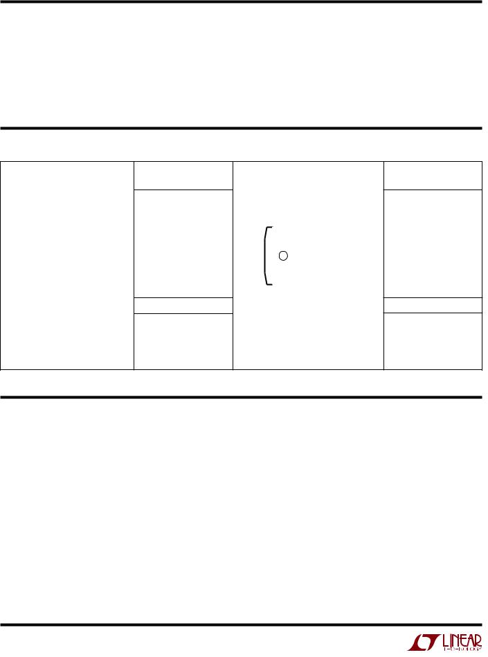
TYPICAL APPLICATIOU
|
Active Terminator for SCSI-2 Bus |
|
|
||
|
|
|
|
110Ω |
|
|
|
|
|
110Ω |
|
|
|
LT1117-2.85 |
|
110Ω |
18 TO 27 |
|
IN |
OUT |
|
||
|
|
|
LINES |
||
4.75V TO |
+ |
GND |
+ |
|
|
|
110Ω |
|
|||
5.25V |
10µF |
22µF |
|
||
|
|
|
|
LT1117 • TA01 |
|
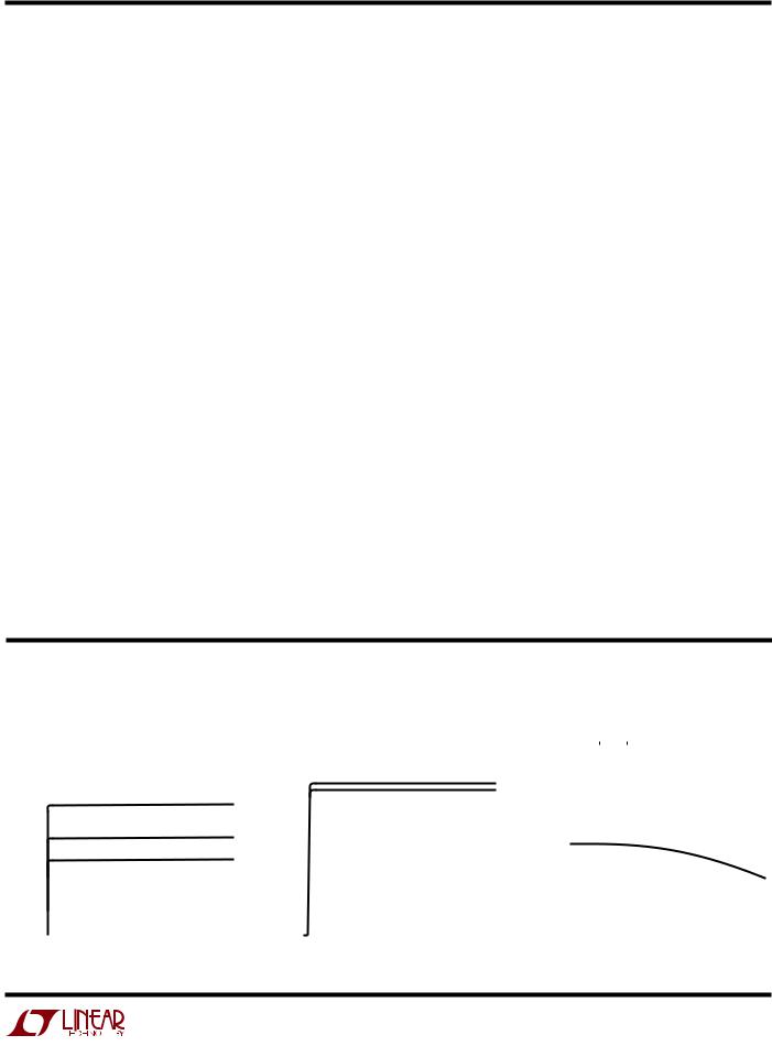
Dropout Voltage (VIN – VOUT)
|
1.4 |
|
–40°C ≤ TJ < 0°C |
|
1.2 |
(V) |
0°C ≤ TJ ≤ 125°C |
1.0 |
|
VOLTAGE |
TJ = 25°C |
0.8 |
|
TJ = 125°C |
|
DROPOUT |
0.6 |
0.4 |
|
|
|
|
0.2 |
 INDICATES GUARANTEED TEST POINT 0


0 |
100 |
200 |
300 |
400 |
500 |
600 |
700 |
800 |
|
|
OUTPUT CURRENT (mA) |
|
|
||||
LT1117 • TPC01
1
LT1117/LT1117-2.85 LT1117-3.3/LT1117-5
ABSOLUTE
WAXIWUW
RATIUGS (Note 1)
Input Voltage |
|
Operating JunctionTemperature Range |
|
Operating Voltage |
|
C Grade ................................................. |
0°C to 125°C |
LT1117, LT1117-3.3, LT1117-5 ...................... |
15V |
I Grade ............................................. |
– 40°C to 125°C |
LT1117-2.85 ................................................... |
10V |
Storage Temperature Range ................. |
– 65°C to 150°C |
Surge Voltage |
|
Lead Temperature ................... |
(See Soldering Methods) |
LT1117, LT1117-3.3, LT1117-5 ...................... |
20V |
|
|
PACKAGE/ORDER IUFORWATIOU
|
FRONT VIEW |
|
||
TAB IS |
|
3 |
|
IN |
|
|
|||
|
2 |
|
OUT |
|
VOUT |
|
|
||
|
1 |
|
ADJ/GND |
|
|
|
|
||
|
|
|
||
|
|
|
|
|
ST PACKAGE
3-LEAD PLASTIC SOT-223
TJ MAX = 125°C,θJC = 15°C/W
ORDER PART
NUMBER
LT1117CST LT1117CST-2.85 LT1117CST-3.3 LT1117CST-5 LT1117IST LT1117IST-2.85 LT1117IST-3.3 LT1117IST-5
ST PART MARKING
1117 1117I
11172 11172I
11173 11173I
11175 11175I
|
|
FRONT VIEW |
|
|
|
|
|
|
|
TAB IS |
3 |
|
IN |
|
|
||||
2 |
|
OUT |
||
VOUT |
|
|||
1 |
|
ADJ/GND |
||
|
|
|||
|
|
|
|
|
|
|
M PACKAGE |
|
|
3-LEAD PLASTIC DD |
|
|||
TJ MAX = 125°C,θJC = 10°C/W |
|
|||
ORDER PART
NUMBER
LT1117CM LT1117CM-2.85 LT1117CM-3.3 LT1117CM-5
DD PART MARKING
1117
11172
11173
11175
Consult factory for Military grade parts.
ELECTRICAL CHARACTERISTICS
The ● denotes specifications which apply over the full operating temperature range, otherwise specifications are at TJ = 25°C.
PARAMETER |
|
CONDITIONS |
|
|
MIN |
TYP |
MAX |
UNITS |
Reference Voltage |
LT1117 |
IOUT = 10mA, (VIN – VOUT) = 2V, TJ = 25°C |
|
1.238 |
1.250 |
1.262 |
V |
|
|
|
10 ≤ IOUT ≤ 800mA, 1.4V ≤ (VIN – VOUT) ≤ 10V |
● |
1.225 |
1.250 |
1.270 |
V |
|
Output Voltage |
LT1117-2.85 |
IOUT = 10mA, VIN = 4.85V, TJ = 25°C |
|
2.820 |
2.850 |
2.880 |
V |
|
|
|
0 ≤ IOUT ≤ 800mA, 4.25V ≤ VIN ≤ 10V |
● |
2.790 |
2.850 |
2.910 |
V |
|
|
|
0 ≤ IOUT ≤ 500mA, VIN = 3.95V |
● |
2.790 |
2.850 |
2.910 |
V |
|
|
LT1117-3.3 |
IOUT = 10mA, VIN = 5V, TJ = 25°C |
|
3.267 |
3.300 |
3.333 |
V |
|
|
|
0 ≤ IOUT ≤ 800mA, 4.75V ≤ VIN ≤ 10V |
● |
3.235 |
3.300 |
3.365 |
V |
|
|
LT1117-5 |
IOUT = 10mA, VIN = 7V, TJ = 25°C |
|
4.950 |
5.000 |
5.050 |
V |
|
|
|
0 ≤ IOUT ≤ 800mA, 6.50V ≤ VIN ≤ 12V |
● |
4.900 |
5.000 |
5.100 |
V |
|
Line Regulation |
LT1117 |
IOUT = 10mA, 1.5V |
≤ VIN – VOUT ≤ 15V (Note 2) |
● |
|
0.035 |
0.2 |
% |
|
LT1117-2.85 |
IOUT = 0mA, 4.25V |
≤ VIN ≤ 10V (Note 2) |
● |
|
1 |
6 |
mV |
|
LT1117-3.3 |
IOUT = 0mA, 4.75V |
≤ VIN ≤ 15V (Note 2) |
● |
|
1 |
6 |
mV |
|
LT1117-5 |
IOUT = 0mA, 6.5V ≤ VIN ≤ 15V (Note 2) |
● |
|
1 |
10 |
mV |
|
2
LT1117/LT1117-2.85
LT1117-3.3/LT1117-5
ELECTRICAL CHARACTERISTICS
The ● denotes specifications which apply over the full operating temperature range, otherwise specifications are at TJ = 25°C.
PARAMETER |
|
CONDITIONS |
|
|
MIN |
TYP |
MAX |
UNITS |
|
|
|
|
|
|
|
|
|
Load Regulation |
LT1117 |
(VIN – VOUT) = 3V, 10mA ≤ IOUT ≤ 800mA (Note 2) |
● |
|
0.1 |
0.4 |
% |
|
|
LT1117-2.85 |
VIN = 4.25V, 0 ≤ IOUT |
≤ 800mA (Note 2) |
● |
|
1 |
10 |
mV |
|
LT1117-3.3 |
VIN = 4.75V, 0 ≤ IOUT |
≤ 800mA (Note 2) |
● |
|
1 |
10 |
mV |
|
LT1117-5 |
VIN = 6.5V, 0 ≤ IOUT ≤ 800mA (Note 2) |
● |
|
1 |
15 |
mV |
|
Dropout Voltage |
|
IOUT = 100mA, 0°C ≤ TJ ≤ 125°C (Note 3) |
|
|
1.00 |
1.10 |
V |
|
|
|
IOUT = 500mA, 0°C ≤ TJ ≤ 125°C (Note 3) |
|
|
1.05 |
1.15 |
V |
|
|
|
IOUT = 800mA, 0°C ≤ TJ ≤ 125°C (Note 3) |
|
|
1.10 |
1.20 |
V |
|
|
|
IOUT = 100mA, – 40°C ≤ TJ < 0°C (Note 3) |
|
|
1.00 |
1.20 |
V |
|
|
|
IOUT = 500mA, – 40°C ≤ TJ < 0°C (Note 3) |
|
|
1.05 |
1.25 |
V |
|
|
|
IOUT = 800mA, – 40°C ≤ TJ < 0°C (Note 3) |
|
|
1.10 |
1.30 |
V |
|
Current Limit |
|
(VIN – VOUT) = 5V, TJ = 25°C, |
|
800 |
950 |
1200 |
mA |
|
Minimum Load Current |
LT1117 |
(VIN – VOUT) = 15V (Note 4) |
● |
|
1.7 |
5 |
mA |
|
Quiescent Current |
LT1117-2.85 |
VIN ≤ 10V |
|
● |
|
5 |
10 |
mA |
|
LT1117-3.3 |
VIN ≤ 15V |
|
● |
|
5 |
10 |
mA |
|
LT1117-5 |
VIN ≤ 15V |
|
● |
|
5 |
10 |
mA |
Thermal Regulation |
|
TA = 25°C, 30ms Pulse |
|
|
0.01 |
0.1 |
%/W |
|
Ripple Rejection |
|
fRIPPLE = 120Hz, (VIN – VOUT) = 3V, VRIPPLE = 1VP-P |
● |
60 |
75 |
|
dB |
|
Adjust Pin Current |
|
|
|
● |
|
55 |
120 |
A |
Adjust Pin Current Change |
|
10mA ≤ IOUT ≤ 800mA, 1.4V ≤ (VIN – VOUT) ≤ 10V |
● |
|
0.2 |
5 |
A |
|
Temperature Stability |
|
|
|
|
|
0.5 |
|
% |
Long Term Stability |
|
TA = 125°C, 1000Hrs |
|
|
|
0.3 |
|
% |
RMS Output Noise |
|
(% of VOUT), 10Hz ≤ f ≤ 10kHz |
|
|
0.003 |
|
% |
|
Thermal Resistance |
|
(Junction-to-Case, at Tab) |
|
|
15 |
|
°C/W |
|
|
|
|
|
|
|
|
|
|
Note 1: Absolute Maximum Ratings are those values beyond which the life to the device may be imparied.
Note 2: See thermal regulation specification for changes in output voltage due to heating effects. Load regulation and line regulation are measured at a constant junction temperature by low duty cycle pulse testing.
Note 3: Dropout voltage is specified over the full output current range of the device. Dropout voltage is defined as the minimum input/output differential measured at the specified output current. Test points and limits are also shown on the Dropout Voltage curve.
Note 4: Minimum load current is defined as the minimum output current required to maintain regulation.
TYPICAL PERFORWAUCE CHARACTERISTICS
|
Minimum Operating Current |
|
|
|
|
|
|
|
|
|
|
|
|
|
|
|
||||||
|
(Adjustable Device) |
|
|
|
|
|
|
|
Short-Circuit Current |
|
|
|
|
|
|
|
||||||
4 |
|
|
|
|
|
|
|
|
|
|
1.25 |
|
|
|
|
|
|
|
|
|
|
|
|
|
|
|
|
|
|
|
|
|
|
|
|
|
|
|
|
|
|
|
|
||
CURRENTOPERATINGMINIMUM(mA) |
|
|
|
|
|
|
|
|
|
|
|
|
|
|
|
|
|
|
|
|
|
|
|
|
|
|
|
|
|
|
|
CURRENTCIRCUITSHORT(A) |
1.00 |
|
|
|
|
|
TJ = 125 |
°C |
|
|
|||
|
|
|
|
|
|
|
|
|
|
|
|
|
|
|
|
|
|
|
|
|||
|
|
|
|
|
|
|
|
|
|
|
|
|
|
|
|
|
|
|
|
|
||
3 |
|
|
|
|
TJ = 125°C |
|
|
|
0.75 |
|
|
|
|
|
TJ = 25°C |
|
|
|
||||
|
|
|
|
|
|
|
|
|
|
|
|
|
|
|
|
|
|
|
||||
|
|
|
|
|
|
|
|
|
|
|
|
|
|
|
|
|
|
|
|
|
|
|
2 |
|
|
|
|
TJ = 25°C |
|
|
|
|
|
|
|
|
|
|
|
|
|
|
|
||
|
|
|
|
|
|
|
|
|
|
|
|
|
|
|
|
|
|
|
|
|||
|
|
|
|
|
|
|
|
|
|
0.50 |
|
|
|
|
|
|
|
|
|
|
|
|
|
|
|
|
|
|
|
|
|
|
|
|
|
|
|
|
|
|
|
|
|
||
|
|
|
|
|
|
|
|
|
|
|
|
|
|
|
|
|
|
|
|
|
|
|
|
|
|
|
|
TJ = –55°C |
|
|
|
|
|
|
|
|
|
|
|
|
|
|
|||
|
|
|
|
|
|
|
|
|
|
|
|
|
|
|
|
|
|
|
|
|||
1 |
|
|
|
|
|
|
|
|
|
|
0.25 |
|
|
|
|
|
|
|
|
|
|
|
|
|
|
|
|
|
|
|
|
|
|
|
|
|
|
|
|
|
|
|
|
||
|
|
|
|
|
|
|
|
|
|
|
|
|
|
|
|
|
|
|
|
|
|
|
|
|
|
|
|
|
|
|
|
|
|
|
|
|
|
|
|
|
|
|
|
|
|
0 |
|
|
|
|
|
|
|
|
|
|
0 |
|
|
|
|
|
|
|
|
|
|
|
5 |
10 |
15 |
|
20 |
|
5 |
|
10 |
|
|
15 |
|||||||||||
0 |
|
|
0 |
|
|
|
||||||||||||||||
|
INPUT/OUTPUT DIFFERENTIAL (V) |
|
|
|
|
INPUT/OUTPUT DIFFERENTIAL (V) |
|
|
||||||||||||||
|
|
|
|
|
|
LT1117 • TPC02 |
|
|
|
|
|
|
|
|
LT1117 • TPC03 |
|||||||
Load Regulation
|
0.10 |
|
|
|
|
|
|
|
|
|
|
|
|
|
|
|
|
|
ILOAD = 800mA |
|
|
|
|
|
|
|
|
|
|
||||
|
|
|
|
|
|
|
|
|
|
|
|
|
||||
(%) |
0.05 |
|
|
|
|
|
|
|
|
|
|
|
|
|
|
|
DEVIATION |
|
|
|
|
|
|
|
|
|
|
|
|
|
|
|
|
0 |
|
|
|
|
|
|
|
|
|
|
|
|
|
|
|
|
VOLTAGE |
|
|
|
|
|
|
|
|
|
|
|
|
|
|
|
|
–0.05 |
|
|
|
|
|
|
|
|
|
|
|
|
|
|
|
|
|
|
|
|
|
|
|
|
|
|
|
|
|
|
|
|
|
OUTPUT |
–0.10 |
|
|
|
|
|
|
|
|
|
|
|
|
|
|
|
|
|
|
|
|
|
|
|
|
|
|
|
|
|
|
||
–0.15 |
|
|
|
|
|
|
|
|
|
|
|
|
|
|
|
|
|
|
|
|
|
|
|
|
|
|
|
|
|
|
|
||
|
–0.20 |
|
|
|
|
|
|
|
|
|
|
|
|
|
|
|
|
|
–25 |
0 |
25 |
50 |
75 |
100 |
125 |
||||||||
|
–50 |
|||||||||||||||
TEMPERATURE (°C)
LT1117 • TPC04
3

LT1117/LT1117-2.85
LT1117-3.3/LT1117-5
TYPICAL PERFORWAUCE CHARACTERISTICS
|
|
LT1117 Ripple Rejection |
|
|
LT1117 Ripple Rejection vs Current |
|
Temperature Stability |
|
|
|
||||||||||||
|
100 |
|
|
|
|
|
|
100 |
VOUT = 5V |
|
|
|
|
2.0 |
|
|
|
|
|
|
|
|
|
90 |
|
VRIPPLE ≤ 3VP-P |
VRIPPLE ≤ |
|
|
90 |
|
|
|
|
|
|
|
|
|
|
|
|
|
||
|
|
0.5VP-P |
|
|
CADJ = 25 F |
|
|
|
|
|
|
|
|
|
|
|
|
|
||||
RIPPLE REJECTION (dB) |
80 |
|
|
|
(VIN – VOUT) ≥ 3V |
RIPPLE REJECTION (dB) |
80 |
COUT = 25 F |
|
fRIPPLE = 120Hz |
|
(%) |
1.0 |
|
|
|
|
|
|
|
|
|
70 |
|
|
|
70 |
|
VRIPPLE ≤ 3VP-P |
|
OUTPUT VOLTAGE CHANGE |
|
|
|
|
|
|
|
|
||||||
|
|
|
|
|
|
|
|
|
|
|
|
|
|
|
|
|||||||
60 |
|
|
|
|
|
60 |
|
|
|
|
|
|
|
|
|
|
|
|
|
|||
50 |
|
|
|
|
|
50 |
|
|
fRIPPLE = 20kHz |
|
0 |
|
|
|
|
|
|
|
|
|||
40 |
|
|
(VIN – VOUT) ≥ VDROPOUT |
|
40 |
|
VRIPPLE ≤ 0.5VP-P |
|
|
|
|
|
|
|
|
|
|
|||||
30 |
|
|
|
|
|
|
|
|
|
|
|
|
|
|
|
|||||||
|
|
|
|
|
30 |
|
|
|
|
–1.0 |
|
|
|
|
|
|
|
|
||||
20 |
|
|
|
|
|
20 |
|
|
|
|
|
|
|
|
|
|
|
|
||||
CADJ = 200 F AT f < 60Hz |
|
|
|
|
|
|
|
|
|
|
|
|
|
|
|
|||||||
|
10 |
CADJ = 25 F AT f > 60Hz |
|
|
|
10 |
|
|
|
|
|
|
|
|
|
|
|
|
|
|
||
|
0 |
IOUT = 0.5A |
|
|
|
|
0 |
|
|
|
|
|
–2.0 |
|
|
|
|
|
|
|
|
|
|
10 |
100 |
1k |
10k |
100k |
|
0.2 |
0.4 |
0.6 |
0.8 |
|
–25 |
0 |
25 |
50 |
75 |
100 |
125 |
150 |
|||
|
|
|
0 |
|
–50 |
|||||||||||||||||
FREQUENCY (Hz) |
OUTPUT CURRENT (A) |
TEMPERATURE (°C) |
LT1117 • TPC05 |
LT1117 • TPC06 |
LT1117 • TPC07 |
AJUST PIN CURRENT ( A)
Adjust Pin Current
100 |
|
|
|
|
|
|
|
|
90 |
|
|
|
|
|
|
|
|
80 |
|
|
|
|
|
|
|
|
70 |
|
|
|
|
|
|
|
|
60 |
|
|
|
|
|
|
|
|
50 |
|
|
|
|
|
|
|
|
40 |
|
|
|
|
|
|
|
|
30 |
|
|
|
|
|
|
|
|
20 |
|
|
|
|
|
|
|
|
10 |
|
|
|
|
|
|
|
|
0 |
–25 |
0 |
25 |
50 |
75 |
100 |
125 |
150 |
–50 |
TEMPERATURE (°C)
LT1117-2.85
Load Transient Response
|
|
0.3 |
CIN = 10 F |
|
|
|
|
|
|
|
|
|
OUPUT VOLTAGE |
|
|
|
|
|
|
|
|
|
|
||
DEVIATION (V) |
0.2 |
COUT = 10 F TANTALUM |
|
|
|
|
|
|||||
|
VIN = 4.25V |
|
|
|
|
|
|
|
|
|||
0.1 |
PRELOAD = 0.1A |
|
|
|
|
|
|
|||||
|
|
|
|
|
|
|
|
|
|
|||
0 |
|
|
|
|
|
|
|
|
|
|
||
|
|
|
|
|
|
|
|
|
|
|
||
|
|
–0.1 |
|
|
|
|
|
|
|
|
|
|
|
|
–0.2 |
|
|
|
|
|
|
|
|
|
|
CURRENT |
|
0.5 |
|
|
|
|
|
|
|
|
|
|
(A) |
0 |
|
|
|
|
|
|
|
|
|
|
|
|
|
|
|
|
|
|
|
|
|
|
||
LOAD |
|
–0.5 |
|
|
|
|
|
|
|
|
|
|
|
0 |
10 |
20 |
30 |
40 |
50 |
60 |
70 |
80 |
90 |
100 |
|
|
|
|||||||||||
TIME ( s)
LT1117-5
Load Transient Response
|
|
0.3 |
CIN = 10 F |
|
|
|
|
|
|
|
|
|
OUPUT VOLTAGE |
|
|
|
|
|
|
|
|
|
|
||
DEVIATION (V) |
0.2 |
COUT = 10 F TANTALUM |
|
|
|
|
|
|||||
|
VIN = 6.5V |
|
|
|
|
|
|
|
|
|||
0.1 |
PRELOAD = 0.1A |
|
|
|
|
|
|
|||||
|
|
|
|
|
|
|
|
|
|
|||
0 |
|
|
|
|
|
|
|
|
|
|
||
|
|
|
|
|
|
|
|
|
|
|
||
|
|
–0.1 |
|
|
|
|
|
|
|
|
|
|
|
|
–0.2 |
|
|
|
|
|
|
|
|
|
|
CURRENT |
|
0.5 |
|
|
|
|
|
|
|
|
|
|
(A) |
0 |
|
|
|
|
|
|
|
|
|
|
|
|
|
|
|
|
|
|
|
|
|
|
||
LOAD |
|
–0.5 |
|
|
|
|
|
|
|
|
|
|
|
0 |
10 |
20 |
30 |
40 |
50 |
60 |
70 |
80 |
90 |
100 |
|
|
|
|||||||||||
TIME ( s)
LT1117 • TPC08 |
LT1117 • TPC09 |
LT1117 • TPC10 |
LT1117-2.8
Line Transient Response
|
|
60 |
CIN = 1 F |
|
|
|
||
OUPUT VOLTAGE |
DEVIATION (mV) |
|
|
|
|
|||
40 |
COUT = 10 F TANTALUM |
|||||||
|
IOUT = 0.1A |
|
|
|
||||
20 |
|
|
|
|
|
|
||
0 |
|
|
|
|
|
|
||
|
|
|
|
|
|
|
||
|
|
–20 |
|
|
|
|
|
|
|
|
–40 |
|
|
|
|
|
|
VOLTAGE |
|
5.25 |
|
|
|
|
|
|
(V) |
4.25 |
|
|
|
|
|
|
|
INPUT |
|
3.25 |
0 |
20 |
40 |
60 |
80 |
100 120 140 160 180 200 |
|
|
|||||||
|
|
|
||||||
TIME ( s)
LT1117-5
Line Transient Response
|
|
60 |
|
CIN = 1 F |
|
|
|
|
OUPUT VOLTAGE |
DEVIATION (mV) |
|
|
|
|
|
||
40 |
|
COUT = 10 F TANTALUM |
||||||
20 |
|
IOUT = 0.1A |
|
|
||||
|
|
|
|
|
|
|||
0 |
|
|
|
|
|
|
||
|
|
|
|
|
|
|
||
|
|
–20 |
|
|
|
|
|
|
|
|
–40 |
|
|
|
|
|
|
VOLTAGE |
|
7.50 |
|
|
|
|
|
|
(V) |
6.50 |
|
|
|
|
|
|
|
INPUT |
|
5.50 |
|
|
|
|
|
|
|
0 |
20 |
40 |
60 |
80 |
100 |
120 140 160 180 200 |
|
|
|
|||||||
TIME ( s)
LT1117 • TPC11 |
LT1117 • TPC12 |
4
 Loading...