


Linear Technology LT1081IN, LT1081CSW, LT1081CN, LT1081CJ, LT1081 Datasheet
...
|
|
|
|
|
|
|
|
|
|
|
|
|
Advanced Low Power |
||
|
|
|
|
|
|
|
|
|
|
|
|
|
|||
|
|
|
|
|
|
|
|
|
|
|
|
|
|||
|
|
|
|
|
|
|
|
|
|
|
|
|
|||
|
|
|
|
|
|
|
|
|
|
|
|
|
|||
|
|
|
|
|
|
|
|
|
|
|
|
5V RS232 Dual Driver/Receiver |
|||
|
FEATURES |
DESCRIPTIOU |
|||||||||||||
|
■ |
Superior to CMOS |
The LT®1080/LT1081 are the only dual RS232 driver/ |
||||||||||||
|
|
– Improved Speed: Operates over 120kBaud |
receiver with charge pump to guarantee absolutely no |
||||||||||||
|
|
– Improved Protection: Outputs Can Be Forced |
latchup. These interface optimized devices provide a real- |
||||||||||||
|
|
to ±30V without Damage |
istic balance between CMOS levels of power dissipation |
||||||||||||
|
|
– Three-State Outputs Are High |
and real world requirements for ruggedness. The driver |
||||||||||||
|
|
Impedance When Off |
outputs are fully protected against overload and can be |
||||||||||||
|
|
– Only Needs 1 F Capacitors |
shorted to ±30V. Unlike CMOS, the advanced architecture |
||||||||||||
|
■ |
Absolutely No Latchup |
of the LT1080/LT1081 does not load the signal line when |
||||||||||||
|
■ |
CMOS Comparable Low Power: 60mW |
“shut down” or when power is off. Both the receiver and |
||||||||||||
|
■ |
Can Power Additional RS232 Drivers: 10mA |
RS232 outputs are put into a high impedance state. An |
||||||||||||
|
■ |
Supply Current in Shutdown: 1 A |
advanced output stage allows driving higher capacitive |
||||||||||||
|
■ |
Available in SO Package |
loads at higher speeds with exceptional ruggedness |
||||||||||||
|
■ |
Available with or without Shutdown |
against ESD. |
||||||||||||
|
APPLICATIOUS |
For applications requiring up to five drivers and five |
|||||||||||||
|
receiverswithchargepumpinonepackageseetheLT1130A |
||||||||||||||
|
|
Portable Computers |
Series data sheet. A version of the LT1080/LT1081, the |
||||||||||||
|
■ |
LT1180A and LT1181A that use only 0.1 F capacitors, is |
|||||||||||||
|
■ |
Battery-Powered RS232 Systems |
also available. All of Linear Technology’s RS232 ICs are |
||||||||||||
|
|
Power Supply Generator |
|||||||||||||
|
■ |
available in standard surface mount packages. |
|||||||||||||
|
■ |
Terminals |
|||||||||||||
|
|
|
|
|
|||||||||||
|
, LTC and LT are registered trademarks of Linear Technology Corporation. |
||||||||||||||
|
■ |
Modems |
|
||||||||||||
|
|
|
|
|
|||||||||||
|
|
|
|
|
|
|
|
|
|
|
|
|
|
|
|
|
|
|
|
|
|
|
|
|
|
|
|
|
|
|
|
TYPICAL APPLICATIOU
|
2 |
|
|
17 |
5V INPUT |
|
|
|
|
|
|
1 F |
4 |
|
|
3 |
|
|
|
|
9V OUTPUT |
||
|
|
|
|
|
|
|
|
LT1080 |
|
|
1 F |
|
|
|
|
|
|
|
5 |
|
|
7 |
–9V OUTPUT |
|
|
|
|
|
|
1 F |
6 |
|
|
|
1 F |
|
|
|
|
|
|
|
12 |
|
|
15 |
RS232 OUTPUT |
|
|
|
|
|
|
LOGIC |
|
|
|
|
|
INPUTS |
11 |
|
|
8 |
RS232 OUTPUT |
|
|
|
|||
|
|
|
|
|
|
|
13 |
|
|
14 |
RS232 INPUT |
|
|
|
|
|
|
LOGIC |
|
|
5k |
|
|
OUTPUTS |
10 |
|
|
9 |
|
|
|
|
RS232 INPUT |
||
|
|
|
|
|
|
|
18 |
|
5k |
16 |
|
ON/OFF |
|
|
|
||
|
|
|
|
|
|
|
|
|
|
|
1080/81 • TA01 |
Supply Generator Outputs
|
10 |
|
|
|
V+ OUTPUT |
|
|
|
|
||
|
8 |
|
|
|
|
|
|
|
|||
|
RL TO V– |
|
|
|
|
|
|
|
|
||
|
6 |
|
|
|
|
RL TO GND |
|
||||
|
|
|
|
|
|
|
|
||||
(V) |
4 |
|
|
|
|
|
|
|
|
|
|
VOLTAGE |
2 |
|
|
|
|
|
|
|
|
|
|
0 |
VCC = 5V |
|
|
|
|
|
|
|
|
||
OUTPUT |
–2 |
|
|
|
|
|
|
|
|
|
|
–4 |
|
|
|
|
|
|
RL TO GND |
|
|||
|
|
|
|
|
|
|
|
||||
|
–6 |
RL TO V+ |
|
|
|
|
|
||||
|
|
|
|
|
|
|
|
|
|||
|
–8 |
|
|
|
V– OUTPUT |
|
|
|
|
||
|
–10 |
|
|
|
|
|
|
|
|||
|
0 |
2 |
4 |
6 |
8 |
10 |
12 |
14 |
16 |
18 |
20 |
|
|
|
|
OUTPUT CURRENT (mA) |
|
|
|
||||
1080/81 TA01a
1
LT1080/LT1081
ABSOLUTE
WAXIWUW
RATIUGS (Note 1)
Supply Voltage (VCC) |
................................................. 6V |
V+ ........................................................................................... |
12V |
V– ....................................................................................... |
– 12V |
Input Voltage |
V – to V+ |
Driver ........................................................... |
|
Receiver ................................................. |
– 30V to 30V |
ON/OFF Pin .............................................. |
GND to 12V |
Output Voltage |
(V – + 30V) to (V + – 30V) |
Driver ................................. |
|
Receiver .................................. |
– 0.3V to (V CC + 0.3V) |
Short-Circuit Duration |
|
V+ ...................................................................................... |
30 sec |
V– ...................................................................................... |
30 sec |
Driver Output ............................................... |
Indefinite |
Receiver Output ........................................... |
Indefinite |
Operating Temperature Range |
0°C to 70°C |
LT1080C/LT1081C ................................. |
|
LT1080I/LT1081I ................................ |
–40°C to 85°C |
LT1080M/LT1081M .......................... |
–55°C to 125°C |
Storage Temperature Range .................. |
–65°C to 150°C |
Lead Temperature (Soldering, 10 sec)................. |
300°C |
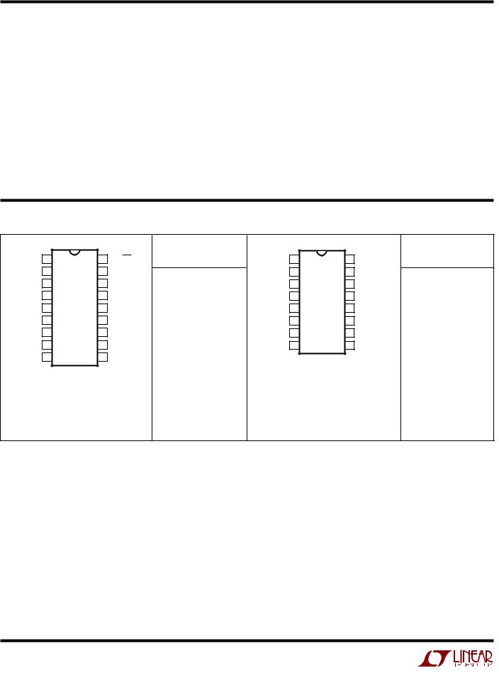
PACKAGE/ORDER IUFORWATIOU
|
TOP VIEW |
|
|
NC |
1 |
18 |
ON/OFF |
C1+ |
2 |
17 |
VCC |
V+ |
3 |
16 |
GND |
C1– |
4 |
15 |
TR1 OUT |
C2+ |
LT1080 |
|
|
5 |
14 |
REC1 IN |
|
C2– |
6 |
13 |
REC1 OUT |
V– |
7 |
12 |
TR1 IN |
TR2 OUT |
8 |
11 |
TR2 IN |
REC2 IN |
9 |
10 |
REC2 OUT |
J PACKAGE |
N PACKAGE |
||
18-LEAD CERDIP |
18-LEAD PDIP |
||
|
SW PACKAGE |
|
|
|
18-LEAD PLASTIC SO WIDE |
|
|
TJMAX = 150°C, θJA = 100°C/W, θJC = 40°C/W (J) TJMAX = 150°C, θJA = 120°C/W, θJC = 50°C/W (N) TJMAX = 150°C, θJA = 90°C/W, θJC = 26°C/W (SW)
ORDER PART
NUMBER
LT1080CJ
LT1080CN
LT1080CSW
LT1080IN
LT1080ISW
LT1080MJ
TOP VIEW
C1+ |
1 |
|
16 |
VCC |
V+ |
2 |
|
15 |
GND |
C1– |
3 |
|
14 |
TR1 OUT |
C2+ |
4 |
LT1081 |
13 |
REC1 IN |
C2– |
5 |
|
12 |
REC1 OUT |
V– |
6 |
|
11 |
TR1 IN |
TR2 OUT |
7 |
|
10 |
TR2 IN |
REC2 IN |
8 |
|
9 |
REC2 OUT |
J PACKAGE |
N PACKAGE |
16-LEAD CERDIP |
16-LEAD PDIP |
SW PACKAGE
16-LEAD PLASTIC SO WIDE
TJMAX = 150°C, θJA = 100°C/W, θJC = 40°C/W (J) TJMAX = 150°C, θJA = 120°C/W, θJC = 50°C/W (N) TJMAX = 150°C, θJA = 95°C/W, θJC = 27°C/W (SW)
ORDER PART
NUMBER
LT1081CJ
LT1081CN
LT1081CSW
LT1081IN
LT1081ISW
LT1081MJ
2

LT1080/LT1081
ELECTRICAL CHARACTERISTICS The ● denotes the specifications which apply over the full operating temperature range, otherwise specifications are at TA = 25°C. (Note 2)
|
|
|
|
|
|
|
|
|
|
|
|
|
|
PARAMETER |
CONDITIONS |
|
|
MIN |
TYP |
MAX |
UNITS |
||||||
Driver |
|
|
|
|
|
|
|
|
|
|
|||
|
|
|
|
|
|
|
|
|
|
|
|
|
|
Output Voltage Swing |
Load = 3k to GND Both Outputs |
Positive |
● |
5 |
7.3 |
|
V |
||||||
|
|
|
|
|
|
|
Negative |
● |
–5 |
–6.5 |
|
V |
|
|
|
|
|
|
|
|
|
|
|||||
Logic Input Voltage Level |
Input Low Level (VOUT = High) |
|
● |
|
1.4 |
0.8 |
V |
||||||
|
|
|
|
|
Input High Level (VOUT = Low) |
|
● |
2 |
1.4 |
|
V |
|
|
Logic Input Current |
VIN ≥ 2V |
|
● |
|
5 |
20 |
µA |
||||||
|
|
|
|
|
VIN ≤ 0.8V |
|
● |
|
5 |
20 |
µA |
|
|
Output Short-Circuit Current |
Sourcing Current, VOUT = 0V |
|
|
9 |
12 |
|
mA |
||||||
|
|
|
|
|
Sinking Current, VOUT = 0V |
|
|
–9 |
–12 |
|
mA |
|
|
Output Leakage Current |
SHUTDOWN (Note 3), VOUT = ±30V |
|
● |
|
10 |
100 |
µA |
|
|||||
Data Rate (Note 6) |
RL = 3k, CL = 2500pF |
|
|
120 |
|
|
kBd |
||||||
|
|
|
|
|
RL = 3k, CL = 1000pF |
|
|
250 |
|
|
kBd |
|
|
Slew Rate |
RL = 3k, CL = 51pF |
|
|
4 |
15 |
30 |
V/µs |
||||||
Receiver |
|
|
|
|
|
|
|
|
|
|
|
||
|
|
|
|
|
|
|
|
|
|
|
|
|
|
Input Voltage Thresholds |
Input Low Threshold |
Commercial |
● |
0.8 |
1.3 |
|
V |
||||||
|
|
|
|
|
|
|
Industrial and Military |
● |
0.2 |
1.3 |
|
V |
|
|
|
|
|
|
|
|
|
|
|
|
|
|
|
|
|
|
|
|
Input High Threshold |
Commercial |
● |
|
1.7 |
2.4 |
V |
||
|
|
|
|
|
|
|
Industrial and Military |
● |
|
1.7 |
3.0 |
V |
|
|
|
|
|
|
|
|
|
|
|
||||
Hysteresis |
|
|
|
● |
0.1 |
0.4 |
1 |
V |
|||||
|
|
|
|
|
|
|
|
|
|||||
Input Resistance |
VIN = ±10V |
|
|
3 |
5 |
7 |
kΩ |
|
|||||
Output Voltage |
Output Low, IOUT = –1.6mA |
|
● |
|
0.2 |
0.4 |
V |
||||||
|
|
|
|
|
Output High, IOUT = 160µA (VCC = 5V) |
● |
3.5 |
4.8 |
|
V |
|
||
Output Short-Circuit Current |
Sinking Current, VOUT = VCC |
|
|
–10 |
–20 |
|
mA |
||||||
|
|
|
|
|
Sourcing Current, VOUT = 0V |
|
|
0.6 |
1 |
|
mA |
|
|
Output Leakage Current |
SHUTDOWN (Note 3), 0V ≤ VOUT ≤ VCC |
● |
|
1 |
10 |
µA |
|||||||
Power Supply Generator (Note 4) |
|
|
|
|
|
|
|
|
|
|
|
||
|
|
|
|
|
|
|
|
|
|
|
|
|
|
V+ Output Voltage |
IOUT = 0mA |
|
|
8.0 |
9.0 |
|
V |
||||||
|
|
|
|
|
IOUT = 10mA |
|
|
7.0 |
8.0 |
|
V |
||
|
|
|
|
|
IOUT = 15mA |
|
|
6.5 |
7.5 |
|
V |
|
|
V– Output Voltage |
IOUT = 0mA |
|
|
–7.5 |
–8.5 |
|
V |
||||||
|
|
|
|
|
IOUT = –10mA |
|
|
–5.5 |
–6.5 |
|
V |
||
|
|
|
|
|
IOUT = –15mA |
|
|
–5.0 |
–6.0 |
|
V |
|
|
Supply Current |
|
|
|
● |
|
12 |
22 |
mA |
|||||
|
|
|
|
|
|
|
|
|
|||||
Supply Leakage Current (VCC) |
SHUTDOWN (Note 3), LT1080 Only |
|
● |
|
1 |
100 |
µA |
|
|||||
|
|
|
|
|
0V ≤ VON/OFF |
≤ 5V, LT1080 Only |
|
|
|
|
|
µA |
|
ON/OFF |
Pin Current |
|
● |
–15 |
|
80 |
|||||||
Supply Rise Time |
(Note 5), LT1080 Only |
|
|
|
1 |
|
ms |
||||||
|
|
|
|
|
|
|
|
|
|
|
|
|
|
Note 1: Absolute Maximum Ratings are those values beyond which the life of a device may be impaired.
Note 2: These parameters apply for 4.5V ≤ VCC ≤ 5.5V and VON/OFF = 3V, unless otherwise specified.
Note 3: VON/OFF = 0.4V for –55°C ≤ TA ≤ 50°C, and VON/OFF = 0.2V for 50°C ≤ TA ≤ 125°C. (LT1080 only)
Note 4: Unless otherwise specified, VCC = 5V, external loading of V+ and V– equals zero and the driver outputs are low (inputs high).
Note 5: Time from either SHUTDOWN high or power on until V+ ≥ 6V and V– ≤ –6V. All external capacitors are 1µF.
Note 6: Data rate operation guaranteed by slew rate, short-circuit current and propagation delay tests.
3

LT1080/LT1081
PIU FUUCTIOUS (Pin numbers refer to LT1080)
C1+; C1–; C2+; C2– (Pins 2, 4, 5, 6): Requires an external capacitor (≥1µF) from C1+ to C1– and another from C2+ to C2–. Pin 2 can be used for connecting a second positive supply. When a separate positive supply is used, C1 can be deleted.
V+ (Pin 3): Positive Supply for RS232 Drivers.
V+ ≈ 2VCC – 1.5V. Requires an exterenal capacitor (≥1µF) for charge storage. May be loaded (up to 15mA) for external system use. Loading does reduce V+ voltage (see graphs). Capacitor may be tied to ground or +5V input supply. With multiple transceivers, the V+ and V– pins may be paralleled into common capacitors.
V– (Pin 7): Negative Supply for RS232 Drivers.
V– ≈ –(2VCC – 2.5V). Requires an external capacitor (≥1µF) for charge stroage. May be loaded (up to –15mA) for external system use. Loading does reduce V– voltage (see graphs). With multiple transceivers, the V+ and V– pins may be paralleled into common capacitors.
TR2 OUT; TR1 OUT (Pins 8, 15): Driver Outputs with RS232 Voltage Levels. Outputs are in a high impedance state when in the SHUTDOWN mode or when power is off (VCC = 0V) to allow data line sharing. Outputs are fully short-circuit protected from (V– + 30V) to (V+ – 30V) with power on, off or in the SHUTDOWN mode. Typical output breakdowns are greater than ±45V and higher applied
voltages will not damage the device if moderately current limited. Shorting one output will affect output from the other.
REC2 IN; REC1 IN (Pins 9, 14): Receiver Inputs. Accepts RS232 voltage levels (±30V) and has 0.4V of hysteresis to provide noise immunity. Input impedance is nominally 5kΩ.
REC2 OUT; REC1 OUT (Pins 10, 13): Receiver Outputs with TTL/CMOS Voltage Levels. Outputs are in a high impedance state when in the SHUTDOWN mode to allow data line sharing. Outputs are fully short-circuit protected to ground or VCC with power on, off or in the SHUTDOWN mode.
TR2 IN; TR1 IN (Pins 11, 12): RS232 Driver Input Pins. Inputs are TTL/CMOS compatible. Inputs should not be allowed to float. Tie unused inputs to VCC.
GND (Pin 16): Ground Pin.
VCC (Pin 17): Input Supply Pin. Supply current drops to zero in the SHUTDOWN mode.
ON/OFF (Pin 18): Contols the operation mode of the LT1080 and is TTL/CMOS compatible. A logic low puts the device in the SHUTDOWN mode which reduces input supply current to zero and places both driver and receiver outputs in a high impedance state. A logic high fully enables the device.
TYPICAL PERFORWAUCE CHARACTERISTICS
Driver Output Voltage |
Supply Generator Outputs |
Supply Generation from VCC |
or Shutdown |
|
10 |
VCC = 5.5V |
|
|
OUTPUT HIGH |
|
|
|
10 |
|
|
|
V+ OUTPUT VOLTAGE |
|
|
|
10 |
|
|
V+ SUPPLY |
|
|
|
|
|
||||||||
|
8 |
|
|
|
|
|
8 |
|
|
|
|
|
|
8 |
|
|
|
|
|
|
|
||||||||||||
|
|
|
|
|
|
|
|
|
|
LOADED TO V– |
|
|
|
|
|
|
|
|
|
|
|
|
|
|
|
|
|
||||||
(V) |
6 |
|
|
|
|
|
|
|
|
|
6 |
LOADED TO GROUND |
|
|
6 |
|
|
|
|
VCC = 5V |
|
|
|
||||||||||
VCC = 4.5V |
|
|
|
|
|
|
|
|
|
|
|
|
|
|
|
|
|
|
|
|
|||||||||||||
|
|
|
|
|
|
|
|
|
|
|
|
|
|
|
|
|
|
|
|
|
|
|
|
|
|||||||||
OUTPUTDRIVERVOLTAGE |
|
|
|
|
|
|
|
|
OUTPUTVOLTAGE (V) |
LOADED TO V+ |
|
|
|
|
|
|
VOLTAGESUPPLY (V) |
–6 |
|
|
|
|
|
|
|
|
|
|
|||||
–6 |
|
|
|
VCC = 5V |
|
|
|
–6 |
|
|
|
|
|
|
|
|
|
|
C1 TO C4 = 1 F |
|
|||||||||||||
|
4 |
|
|
|
|
|
|
|
4 |
|
|
|
|
|
|
|
|
|
|
|
4 |
|
|
|
|
|
|||||||
|
2 |
|
|
|
|
|
|
|
|
|
2 |
|
|
|
|
|
|
|
|
|
|
|
2 |
|
|
|
|
|
|
|
|
|
|
|
0 |
RL = 3k |
|
|
|
|
|
|
|
0 |
VCC = 5V |
|
|
|
|
|
|
|
|
|
0 |
|
|
|
|
|
|
|
|
|
|
||
|
–2 |
|
|
|
VCC = 5V |
|
|
|
|
–2 |
|
|
|
|
|
|
|
|
|
|
|
–2 |
|
|
|
|
|
|
|
|
|
|
|
|
–4 |
|
|
|
|
|
|
|
–4 |
|
|
|
|
|
|
|
|
|
|
|
–4 |
|
|
|
|
|
|
|
|
|
|
||
|
VCC = 4.5V |
|
|
|
|
|
|
|
|
|
|
|
LOADED TO GROUND |
|
|
|
|
|
|
|
|
|
|
|
|
||||||||
|
|
|
|
|
|
|
|
|
|
|
|
|
|
|
|
|
|
|
|
|
|
|
|
|
|
|
|||||||
|
–8 |
VCC = 5.5V |
|
|
OUTPUT LOW |
|
|
|
–8 |
|
|
|
V– OUTPUT VOLTAGE |
|
|
|
–8 |
|
|
V– SUPPLY |
|
|
|
|
|
||||||||
|
–10 |
|
|
|
|
|
–10 |
|
|
|
|
|
|
–10 |
|
|
|
|
|
|
|
||||||||||||
|
–55 |
–25 |
0 |
25 |
50 |
75 |
100 |
125 |
|
0 |
2 |
4 |
6 |
8 |
10 |
12 |
14 |
16 |
18 |
20 |
|
0 |
0.2 |
0.4 |
0.6 |
0.8 |
1.0 |
1.2 |
1.4 |
1.6 |
1.8 |
2.0 |
|
|
|
|
|
TEMPERATURE (°C) |
|
|
|
|
|
|
OUTPUT CURRENT (mA) |
|
|
|
|
|
|
|
|
TIME (ms) |
|
|
|
|
|||||||||
|
|
|
|
|
|
|
|
1080/81 G01 |
|
|
|
|
|
|
|
|
|
|
1080/81 G02 |
|
|
|
|
|
|
|
|
|
|
1080/81 G03 |
|||
4 |
|
|
|
|
|
|
|
|
|
|
|
|
|
|
|
|
|
|
|
|
|
|
|
|
|
|
|
|
|
|
|
|
|
 Loading...