


LTC1278-4ISW
Linear Technology LTC1278-4ISW, LTC1278-4IN, LTC1278-4CSW, LTC1278-4CN, LTC1278-5CN Datasheet
...
LTC1278
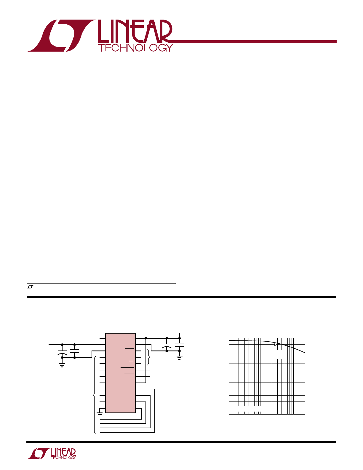
INPUT FREQUENCY (Hz)
10k
0
EFFECTIVE NUMBER OF BITS
S/(N+D) (dB)
3
5
7
10
100k 1M 2M
LT1278 G4
1
4
6
9
12
11
62
56
74
68
8
2
f
SAMPLE
= 500kHz
NYQUIST
FREQUENCY
12-Bit, 500ksps Sampling
A/D Converter with Shutdown
EATU
F
■
Single Supply 5V or ±5V Operation
■
Two Speed Grades,500ksps (LTC1278-5)
RE
S
400ksps (LTC1278-4)
■
70dB S/(N + D) and 74dB THD at Nyquist
■
No Missing Codes Over Temperature
■
75mW (Typ) Power Dissipation
■
Power Shutdown with Instant Wake-Up
■
Internal Reference Can Be Overdriven Externally
■
Internal Synchronized Clock; No Clock Required
■
High Impedance Analog Input
■
0V to 5V or ±2.5V Input Range
■
New Flexible, Friendly Parallel Interface to DSPs
and FIFOs
■
24-Pin Narrow PDIP and SW Packages
U
O
PPLICATI
A
■
High Speed Data Acquisition
■
Digital Signal Processing
■
Multiplexed Data Acquisition Systems
■
Audio and Telecom Processing
■
Spectrum Analysis
, LTC and LT are registered trademarks of Linear Technology Corporation.
S
DUESCRIPTIO
The LTC®1278 is a 1.6µ s, 500ksps, sampling 12-bit A/D
converter that draws only 75mW from a single 5V or ±5V
supplies. This easy-to-use device comes complete with
a 200ns sample-and-hold, a precision reference and an
internally trimmed clock. Unipolar and bipolar conversion modes add to the flexibility of the ADC. The low
power dissipation is made even more attractive by a
8.5mW power-down feature. Instant wake-up from shutdown allows the converter to be powered down even
during brief inactive periods.
The LTC1278 converts 0V to 5V unipolar inputs from a
single 5V supply and ±2.5V bipolar inputs from ±5V
supplies. Maximum DC specs include ±1LSB INL and
±1LSB DNL. Outstanding guaranteed AC performance
includes 70dB S/(N + D) and 78dB THD at the input
frequency of 100kHz over temperature.
The internal clock is trimmed for 1.6µs conversion time.
The clock automatically synchronizes to each sample
command, eliminating problems with asynchronous clock
noise found in competitive devices. A separate convert
start input and a data ready signal (BUSY) ease connections to FIFOs, DSPs and microprocessors.
Single 5V Supply, 500kHz, 12-Bit Sampling A/D Converter
2.42V
REFERENCE
OUTPUT
10µF
A
PPLICATITYPICAL
+
ANALOG INPUT
(0V TO 5V)
0.1µF
12-BIT
PARALLEL
BUS
10
11
12
1
AIN
2
V
3
AGND
4
D11(MSB)
5
D10
6
D9
7
D8
8
D7
9
D6
D5
D4
DGND
O
LTC1278-5
REF
CONVST
U
AV
BUSY
SHDN
DV
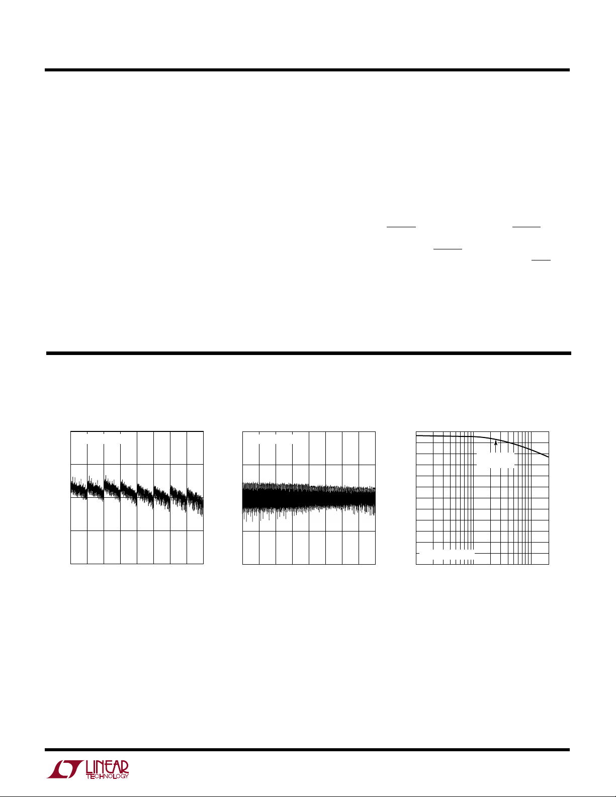
Effective Bits and Signal-to-(Noise + Distortion)
24
DD
23
V
RD
SS
CS
DD
D0
D1
D2
D3
10µF
22
21
µP CONTROL
20
LINES
19
CONVERSION START INPUT
18
POWER DOWN INPUT
17
16
15
14
13
LTC1278 • TA01
5V
+
0.1µF
vs Input Frequency
1
LTC1278
WU
U
PACKAGE
/
O
RDER I FOR ATIO
W
O
A
AVDD = DVDD = VDD (Notes 1, 2)
LUTEXI T
S
A
WUW
ARB
U
G
I
S
Supply Voltage (VDD).............................................. 12V
Negative Supply Voltage (VSS)
Bipolar Operation Only .......................... – 6V to GND
Total Supply Voltage (VDD to VSS)
Bipolar Operation Only ....................................... 12V
Analog Input Voltage (Note 3)
Unipolar Operation ................... – 0.3V to VDD + 0.3V
Bipolar Operation............... VSS – 0.3V to VDD + 0.3V
Digital Input Voltage (Note 4)
Unipolar Operation ................................–0.3V to 12V
Bipolar Operation........................... VSS – 0.3V to 12V
Digital Output Voltage
Unipolar Operation ................... –0.3V to VDD + 0.3V
Bipolar Operation................ VSS – 0.3V to VDD + 0.3V
Power Dissipation............................................. 500mW
Operating Temperature Range
LTC1278-4C, LTC1278-5C ..................... 0°C to 70°C
LTC1278-4I ....................................... –40°C to 85°C
Storage Temperature Range ................ –65°C to 150°C
Lead Temperature (Soldering, 10 sec)................. 300°C
TOP VIEW
A
1
IN
V
2
REF
AGND
3
D11 (MSB)
Consult factory for Military grade parts.
4
D10
5
D9
6
D8
7
D7
8
D6
9
D5
10
D4
11
DGND
12
N PACKAGE
24-LEAD PDIP
T
= 110°C, θJA = 100°C/W (N)
JMAX
T
= 110°C, θJA = 130°C/W (SW)
JMAX
24-LEAD PLASTIC SO WIDE
AVDD
24
V
23
SS
BUSY
22
CS
21
RD
20
CONVST
19
SHDN
18
DV
17
D0
16
D1
15
D2
14
D3
13
SW PACKAGE
DD
ORDER
PART NUMBER
LTC1278-4CN
LTC1278-5CN
LTC1278-4IN
LTC1278-4CSW
LTC1278-5CSW
LTC1278-4ISW
U
With Internal Reference (Notes 5, 6)
LTC1278-4/LTC1278-5
● ±6 LSB
LTC1278-4/LTC1278-5
U
IN
IN
VERTER
CCHARA TERIST
= 0 ● ±10 ±45 ppm/°C
OUT(REF)
ICS
U
PUT
LOG
Analog Input Range (Note 9) 4.95V ≤ VDD ≤ 5.25V (Unipolar) ● 0 to 5 V
Analog Input Leakage Current CS = High ● ±1 µA
Analog Input Capacitance Between Conversions (Sample Mode) 45 pF
IA
(Note 5)
4.75V ≤ VDD ≤ 5.25V, –5.25V ≤ VSS ≤ – 2.45V (Bipolar) ● ±2.5 V
During Conversions (Hold Mode) 5 pF
CO
PARAMETER CONDITIONS MIN TYP MAX UNITS
Resolution (No Missing Codes) ● 12 Bit
Integral Linearity Error (Note 7) ● ±1 LSB
Differential Linearity Error ● ±1 LSB
Offset Error (Note 8) ±4 LSB
Gain Error ±15 LSB
Gain Error Tempco I
A
SYMBOL PARAMETER CONDITIONS MIN TYP MAX UNITS
V
I
IN
C
2
LTC1278
W
U
IC
DY
SYMBOL PARAMETER CONDITIONS MIN TYP MAX UNITS
S/(N + D) Signal-to-Noise Plus Distortion Ratio 100kHz Input Signal ● 70 72 dB
THD Total Harmonic Distortion 100kHz Input Signal ● –80 –78 dB
IMD Intermodulation Distortion f
A
ACCURACY
First 5 Harmonics 250kHz Input Signal –74 dB
Peak Harmonic or Spurious Noise 100kHz Input Signal ● –84 –78 dB
Full Power Bandwidth 4 MHz
Full Linear Bandwidth (S/(N + D) ≥ 68dB) 350 kHz
(Note 5)
LTC1278-4/LTC1278-5
250kHz Input Signal 70 dB
250kHz Input Signal –74 dB
= 99.37kHz, f
IN1
= 249.37kHz, f
f
IN1
= 102.4kHz –82 dB
IN2
= 252.4kHz –70 dB
IN2
U
I TER AL REFERE CE CHARACTERISTICS
PARAMETER CONDITIONS MIN TYP MAX UNITS
V
REF
V
REF
V
REF
V
REF
DIGITAL I PUTS A D DIGITAL OUTPUTS
SYMBOL PARAMETER CONDITIONS MIN TYP MAX UNITS
V
IH
V
IL
I
IN
C
IN
V
OH
V
OL
I
OZ
C
OZ
I
SOURCE
I
SINK
UU
(Note 5)
LTC1278-4/LTC1278-5
Output Voltage I
Output Tempco I
Line Regulation 4.95V ≤ VDD ≤ 5.25V 0.01 LSB/V
Load Regulation 0V ≤ |I
U
High Level Input Voltage V
Low Level Input Voltage VDD = 4.95V ● 0.8 V
Digital Input Current VIN = 0V to V
Digital Input Capacitance 5pF
High Level Output Voltage VDD = 4.95V
Low Level Output Voltage VDD = 4.95V
High Z Output Leakage D11 to D0 V
High Z Output Capacitance D11 to D0 CS High (Note 9 ) ● 15 pF
Output Source Current V
Output Sink Current V
= 0 2.400 2.420 2.440 V
OUT
= 0 ● ±10 ±45 ppm/°C
OUT
–5.25V ≤ V
≤ –4.95V 0.01 LSB/V
SS
| ≤ 1mA 2 LSB/mA
OUT
U
(Note 5)
LTC1278-4/LTC1278-5
= 5.25V ● 2.4 V
DD
DD
IO = –10µA 4.7 V
IO = –200µA ● 4V
IO = 160µA 0.05 V
IO = 1.6mA ● 0.10 0.4 V
= 0V to VDD, CS High ● ±10 µA
OUT
= 0V –10 mA
OUT
= V
OUT
DD
● ±10 µA
10 mA
3
LTC1278
U
W
POWER REQUIRE E TS
SYMBOL PARAMETER CONDITIONS MIN TYP MAX UNITS
V
DD
V
SS
I
DD
I
SS
P
D
Positive Supply Voltage (Notes 10, 11) Unipolar 4.95 5.25 V
Negative Supply Voltage (Note 10) Bipolar Only –2.45 –5.25 V
Positive Supply Current f
Negative Supply Current f
Power Dissipation f
W
U
TI I G CHARACTERISTICS
SYMBOL PARAMETER CONDITIONS MIN TYP MAX UNITS
f
SAMPLE(MAX)
t
SAMPLE(MIN)
t
CONV
t
ACQ
t
1
t
2
t
3
t
4
t
5
t
6
t
7
t
8
t
9
t
10
t
11
t
12
Maximum Sampling Frequency LTC1278-4 ● 400 kHz
Minimum Throughput Time LTC1278-4 ● 2.5 µs
(Acquisition Time Plus Conversion Time) LTC1278-5 ● 2.0 µs
Conversion Time LTC1278-4 2.0 2.3 µs
Acquisition Time 200 ns
CS↓ to RD↓ Setup Time (Notes 9, 10) ● 0ns
CS↓ to CONVST↓ Setup Time (Notes 9, 10) ● 20 ns
SHDN↑ to CONVST↓ Wake-Up Time (Note 10) 350 ns
CONVST Low Time (Notes 10, 12) ● 40 ns
CONVST↓ to BUSY↓ Delay CL = 100pF 40 110 ns
Data Ready Before BUSY↑ CL = 100pF ● 20 40 ns
Wait Time RD↓ After BUSY↑ Mode 2, (see Figure 14) (Note 9) ● –20 ns
Data Access Time After RD↓ CL = 20pF (Note 9) 50 90 ns
Bus Relinquish Time 20 30 75 ns
RD Low Time (Note 9) ● t
CONVST High Time (Notes 9, 12) ● 40 ns
Aperture Delay of Sample-and-Hold Jitter <50ps 15 ns
(Note 5)
LTC1278-4/LTC1278-5
Bipolar 4.75 5.25 V
= 500ksps ● 15.0 29.5 mA
SAMPLE
SHDN = 0V ● 1.7 3.0 mA
= 500ksps, VSS = –5V ● 0.12 0.30 mA
SAMPLE
= 500ksps ● 75.0 150 mW
SAMPLE
SHDN = 0V ● 8.5 15 mW
(Note 5)
LTC1278-4/LTC1278-5
LTC1278-5 ● 500
LTC1278-5 1.6 1.85 µs
Commercial
Industrial ● 140 ns
Commercial
Industrial ● 120 ns
CL = 100pF 70 125 ns
Commercial
Industrial ● 170 ns
Commercial
Industrial ● 20 90 ns
● 130 ns
● 110 ns
● 150 ns
● 20 85 ns
8
ns
4
W
INPUT FREQUENCY (Hz)
10k
0
EFFECTIVE NUMBER OF BITS
S/(N+D) (dB)
3
5
7
10
100k 1M 2M
LT1278 G4
1
4
6
9
12
11
62
56
74
68
8
2
f
SAMPLE
= 500kHz
NYQUIST
FREQUENCY
U
TI I G CHARACTERISTICS
LTC1278
(Note 5)
The ● indicates specifications which apply over the full operating
temperature range; all other limits and typicals TA = 25°C.
Note 1: Absolute Maximum Ratings are those values beyond which the life
of a device may be impaired.
Note 2: All voltage values are with respect to ground with DGND and
AGND wired together (unless otherwise noted).
Note 3: When these pin voltages are taken below V
(ground for unipolar
SS
mode) or above VDD, they will be clamped by internal diodes. This product
can handle input currents greater than 60mA below VSS (ground for
unipolar mode) or above VDD without latch-up.
Note 4: When these pin voltages are taken below V
(ground for unipolar
SS
mode), they will be clamped by internal diodes. This product can handle
input currents greater than 60mA below VSS (ground for unipolar mode)
without latch-up. These pins are not clamped to VDD.
Note 5: AVDD = DVDD = VDD = 5V, (VSS = –5V for bipolar mode), f
SAMPLE
400kHz (LTC1278-4), 500kHz (LTC1278-5), tr = tf = 5ns unless otherwise
Note 7: Integral nonlinearity is defined as the deviation of a code from a
straight line passing through the actual endpoints of the transfer curve. The
deviation is measured from the center of the quantization band.
Note 8: Bipolar offset is the offset voltage measured from –1/2LSB when
the output code flickers between 0000 0000 0000 and 1111 1111 1111.
Note 9: Guaranteed by design, not subject to test.
Note 10: Recommended operating conditions.
Note 11: A
must not exceed VDD or fall below VSS by more than 50mV for
IN
specified accuracy. Therefore the minimum supply voltage for the unipolar
mode is 4.95V. The minimum for the bipolar mode is 4.75V, –2.45V.
Note 12: The falling CONVST edge starts a conversion. If CONVST returns
high at a bit decision point during the conversion it can create small errors.
For best performance ensure that CONVST returns high either within 120ns
after conversion start (i.e., before the first bit decision) or after BUSY rises
(i.e., after the last bit test). See mode 1a and 1b (Figures 12 and 13) timing
=
diagrams.
specified.
Note 6: Linearity, offset and full-scale specifications apply for unipolar and
bipolar modes.
W
U
TYPICAL PERFORMANCE CHARACTERISTICS
Integral Nonlinearity vs
Output Code
1.0
f
SAMPLE
0.5
0
INL ERROR (LSB)
–0.5
–1.0
512 1024 1536 2048
0
= 500kHz
2560 3072 3584 4096
CODE
LT1278 G1
Differential Nonlinearity vs
Output Code
1.0
f
= 500kHz
SAMPLE
0.5
0
DNL ERROR (LSB)
–0.5
–1.0
0
512 1024 1536 2048
CODE
ENOBs and S/(N + D) vs
Input Frequency
2560 3072 3584 4096
LT1278 G2
5
 Loading...