


February 2007
Instrumentation Circuitry Using RMS-to-DC Converters
RMS Converters Rectify Average Results
Jim Williams
INTRODUCTION
It is widely acknowledged that RMS (Root of the Mean of the Square) measurement of waveforms furnishes the most accurate amplitude information.1 Rectify-and- average schemes, usually calibrated to a sine wave, are only accurate for one waveshape. Departures from this waveshaperesultinpronouncederrors.Althoughaccurate, RMS conversion often entails limited bandwidth, restricted range, complexity and difficult to characterize dynamic and static errors. Recent developments address these issues while simultaneously improving accuracy. Figure 1 showstheLTC®1966/LTC1967/LTC1968devicefamily.Low frequency accuracy, including linearity and gain error, is inside 0.5% with 1% error at bandwidths extending to 500kHz. These converters employ a sigma-delta based computational scheme to achieve their performance.2
Figure 2’s pinout descriptions and basic circuits reveal an easily applied device. An output filter capacitor is all that is required to form a functional RMS-to-DC converter. Split and single supply powered variants are shown. Such ease of implementation invites a broad range of application; examples begin with Figure 3.
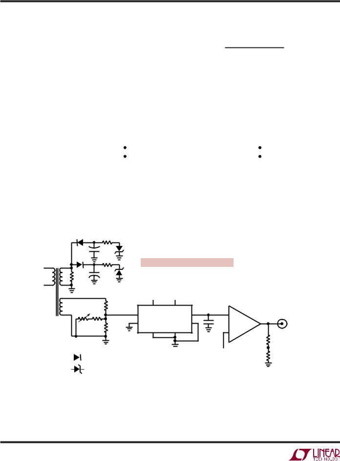
Isolated Power Line Monitor
BEFORE PROCEEDING ANY FURTHER, THE READER IS WARNED THAT CAUTION MUST BE USED IN THE CONSTRUCTION, TESTING AND USE OF THIS CIRCUIT. HIGH VOLTAGE, LETHAL POTENTIALS ARE PRESENT IN THIS CIRCUIT. EXTREME CAUTION MUST BE USED IN WORKINGWITH,ANDMAKINGCONNECTIONSTO,THIS CIRCUIT. REPEAT: THIS CIRCUIT CONTAINS DANGEROUS, HIGH VOLTAGE POTENTIALS. USE CAUTION.
Figure 3’s AC power line monitor has 0.5% accuracy over a sensed 90VAC to 130VAC input and provides a safe, fully isolated output. RMS conversion provides accurate reporting of AC line voltage regardless of waveform distortion, which is common.
 , LT, LTC and LTM are registered trademarks of Linear Technology Corporation. All other trademarks are the property of their respective owners.
1See Appendix A, “RMS-to-DC Conversion” for complete discussion of RMS measurement.
2Appendix A details sigma-delta based RMS-to-DC converter operation.
|
LINEARITY |
CONVERSION |
1% ERROR |
3dB ERROR |
|
|
|
PART NUMBER |
ERROR |
GAIN ERROR |
BANDWIDTH |
BANDWIDTH |
SUPPLY VOLTAGE |
ISUPPLY |
|
TYP/MAX (%) |
TYP/MAX (%) |
(kHz) |
(kHz) |
MIN(V) |
MAX(V) |
MAX (µA) |
|
LTC1966 |
0.02/0.15 |
0.1/0.3 |
6 |
800 |
2.7 |
±5 |
170 |
|
|
|
|
|
|
|
|
LTC1967 |
0.02/0.15 |
0.1/0.3 |
200 |
4MHz |
4.5 |
5.5 |
390 |
|
|
|
|
|
|
|
|
LTC1968 |
0.02/0.15 |
0.1/0.3 |
500 |
15MHz |
4.5 |
5.5 |
2.3mA |
|
|
|
|
|
|
|
|
Figure 1. Primary Differences in RMS to DC Converter Family are Bandwidth and Supply Requirements. All Devices Have Rail-to-Rail Differential Inputs and Output
an106f
AN106-1
Application Note 106
|
|
|
|
|
|
|
|
|
|
|
|
|
|
|
|
|
|
|
|
|
|
|
|
POSITIVE SUPPLY |
|
|
|
|
|
|
|
|
|
|
|
|
|
|
|
|
|
|
|
|
|
|
|
|
|
|
|
|
|
|
|
|
|
|||||||
|
|
|
|
|
|
|
|
|
|
|
|
|
|
|
|
|
|
|
|
|
|
|
|
2.7V TO 5.5V |
|
|
|
|
|
|
|
|
|
|
|
|
|
|
|
|
|
|
|
|
|
|
|
|
|
|
|
|
|
|
|
|
|
|
|
|
|
|
|
|
|
|
|
|
|
|
|
|
|
|
|
|
|
|
|
|
|
|
|
|
|
|
DEPENDING ON DEVICE CHOICE |
|
|
|
|
|
|
|
|
|
|
|
|
|
|
|
|
|
|
|
|
|
|
|
|
|
|
|
|
|
|
|
|
|
|||||||||
|
|
|
|
|
|
|
|
|
|
|
|
|
|
|
|
|
|
|
|
|
|
|
|
|
|
|
|
|
|
|
|
|
|
|
|
|
|
|
|
|
|
|
|
|
|
|
|
|
|
|
|
|
|
|
|
|
|
|
|
|
|
|
|
|
|
|
|
|
|
|
|
|
|
|
|
|
|
|
|
|
|
|
|
|
|
|
|
|
|
|
|
|
|
|
|
|
|
|
|
|
|
|
|
|
|
|
|
|
|
|
|
|
|
|
|
|
|
|
|
|
|
|
|
|
|
|
|
|
|
|
|
DIFFERENTIAL |
|
|
|
|
|
|
+V |
|
|
|
|
|
|
|
|
|
|
OUTPUT TO FILTER CAPACITOR |
||||||||||||||||||||||||||||||||||||||||||||
|
|
|
|
|
|
|
|
|
|
|
|
|
|
|
|
|
|
|
||||||||||||||||||||||||||||||||||||||||||||||
|
|
|
INPUTS. |
|
|
|
|
|
|
|
|
|
|
|
|
|
|
|
|
|
|
|
|
|
|
|
|
|||||||||||||||||||||||||||||||||||||
|
|
|
|
|
|
|
|
|
|
|
INPUT 1 |
LTC1966 |
|
OUTPUT |
|
|
|
|
|
|
|
|
|
|
|
|
|
|
|
|
|
|
|
|
|
|
|
|
|
|
|
|
|
|
|
|
OUTPUT |
|||||||||||||||||
MAX COMMON MODE |
|
|
|
|
|
|
|
|
|
|
|
|
|
|
|
|
|
|
|
|
|
|
|
|
|
|
|
|
|
|
|
|
|
|
|
|
|
|
|
|
|
|
|
|
|
|||||||||||||||||||
RANGE = ±V SUPPLY. |
|
|
|
|
|
|
LTC1967 |
|
|
|
|
|
|
|
|
|
|
OUTPUT REFERRED |
|
|
|
|
|
|
|
|
|
|
||||||||||||||||||||||||||||||||||||
|
|
INPUT 2 |
LTC1968 |
OUTPUT RETURN |
|
|
|
|
|
|
|
|
|
|
|
|
|
|
||||||||||||||||||||||||||||||||||||||||||||||
MAX DIFFERENTIAL = 1V. |
|
|
|
|
|
|
|
|
|
|
|
|
TO THIS PIN. |
|
|
|
|
|
|
|
|
|
|
|||||||||||||||||||||||||||||||||||||||||
|
|
|
|
|
|
|
|
|
|
|
|
|
|
|
|
|
|
|
|
|
|
|
|
|||||||||||||||||||||||||||||||||||||||||
MINIMUM INPUT = 5mV |
|
|
ENABLE |
–V* |
GND |
|
|
|
|
NORMALLY GROUNDED |
|
|
|
|
|
|||||||||||||||||||||||||||||||||||||||||||||||||
|
|
|
|
|
|
|
|
|
|
|
|
|
|
|
|
|
|
|
|
|
|
|
|
|
|
|
|
|
|
|
|
|
|
|
|
|
|
|
|
|
|
|
|
|
|
|
|
|
|
|
|
|
|
|||||||||||
|
|
|
|
|
|
|
|
|
|
|
|
|
|
|
|
|
|
|
|
|
|
|
|
|
|
|
|
|
|
|
|
|
|
|
|
|
|
|
|
|
|
|
|
|
|
|
|
|
|
|
|
|
|
|
|
|
|
|
|
|
|
|
||
|
|
|
|
|
|
|
|
|
|
|
|
|
|
|
|
|
|
|
|
|
|
|
|
|
|
|
|
|
|
|
|
|
|
|
|
|
|
|
|
|
|
|
|
|
|
|
|
|
|
|
|
|
|
|
|
|
|
|
|
|
|
|
|
|
|
|
|
|
|
|
|
|
|
|
|
|
|
|
|
|
|
|
|
|
|
SET HIGH TO |
LTC1966 ONLY. |
POWER |
*NO –V PIN ON THE LTC1967/LTC1968 |
||||||||||||||||||||||||||||||||||||||||
|
|
|
|
|
|
|
|
|
|
|
|
|
|
|
|
|
|
|
|
|
SHUT DOWN |
0V TO –5V |
GROUND |
|
|
|
|
|
|
|
|
|
|
|
|
|
|
|
|
|
|
|
|
|
|
|
|
|
|
|
|
|
|
|
|
|
||||||||
|
|
|
|
|
|
|
|
|
|
|
|
|
|
|
|
|
|
|
|
|
|
|
|
SUPPLY |
|
|
|
|
|
|
|
|
|
|
|
|
|
|
|
|
|
|
|
|
|
|
|
|
|
|
|
|
|
|
|
|
|
|
|
|
|
|
|
|
±5V Supplies, Differential, DC-Coupled |
|
|
5V Single Supply, Differential, AC-Coupled |
|||||||||||||||||||||||||||||||||||||||||||||||||||||||||||||
|
|
RMS-to-DC Converter |
|
|
|
|
|
|
RMS-to-DC Converter |
|
|
|
|
|
|
|
|
|
|
|||||||||||||||||||||||||||||||||||||||||||||
|
|
|
|
|
5V |
|
|
|
|
|
|
|
|
|
|
|
|
|
|
|
|
|
|
|
5V |
|
|
|
|
|
|
|
|
|
|
|||||||||||||||||||||||||||||
|
|
|
|
|
|
|
|
|
|
|
|
|
|
|
|
|
|
|
|
|
|
|
|
|
|
|
|
|
|
|
|
|
|
|
|
|
|
|
|
|
|
|
|
|
|
|
|
|
|
|
|
|
|
|
|
|
|
|
|
|
|
|
|
|
|
|
|
|
|
VDD |
|
|
|
|
|
|
|
|
|
|
|
|
|
|
|
|
|
|
VDD |
|
|
|
|
|
|
|
|
|
|
|
|||||||||||||||||||||||||||||
DC + AC |
|
|
LTC1966 |
|
|
|
DC OUTPUT |
|
|
|
|
|
|
|
|
|
|
LTC1966 |
|
|
|
|
|
|
|
DC OUTPUT |
||||||||||||||||||||||||||||||||||||||
|
IN1 |
|
|
|
|
|
|
|
VOUT |
|
|
|
AC INPUTS |
|
|
|
|
IN1 |
|
|
|
|
|
|
|
VOUT |
|
|
|
|
|
|
|
|||||||||||||||||||||||||||||||
INPUTS |
|
|
|
|
|
|
|
|
|
|
|
CAVE ZO = 85kΩ |
(1VPEAK |
|
|
|
|
|
|
|
|
|
|
|
CAVE |
|
ZO = 85kΩ |
|||||||||||||||||||||||||||||||||||||
(1VPEAK |
|
|
IN2 |
OUT RTN |
|
|
|
|
IN2 |
|
OUT RTN |
|
|
|||||||||||||||||||||||||||||||||||||||||||||||||||
|
|
|
1µF |
|
DIFFERENTIAL) |
|
|
|
|
|
|
1µF |
|
|
|
|
|
|||||||||||||||||||||||||||||||||||||||||||||||
DIFFERENTIAL) |
|
VSS GND |
|
|
|
|
|
|
|
|
|
|
|
|
|
|
|
|
|
|
|
|
VSS GND |
|
|
|
|
|
|
|
|
|
|
|
|
|
|
|
|
|
|
|||||||||||||||||||||||
|
|
|
EN |
|
|
|
|
|
|
|
|
|
|
|
|
|
|
|
|
EN |
|
|
|
|
|
|
|
|
|
|
|
|
||||||||||||||||||||||||||||||||
|
|
|
|
|
|
|
|
|
|
|
|
|
|
CC |
|
|
|
|
|
|
|
|
|
|
|
|
|
|
|
|
||||||||||||||||||||||||||||||||||
|
|
|
|
|
|
|
|
|
|
|
|
|
|
|
|
|
|
|
|
|
|
|
|
|
|
|
|
|
0.1µF |
|
|
|
|
|
|
|
|
|
|
|
|
|
|
|
|
|
|
|
|
|
AN106 F02 |
|
|
|
|
|
|
|
|
|
|
|||
|
|
|
–5V |
|
|
|
|
|
|
|
|
|
|
|
|
|
|
|
|
|
|
|
|
|
|
|
|
|
|
|
|
|
|
|
|
|
|
|
|
|
|
|
|
|
|
|
|
|
|
|
|
|
|
|
|
|
|
|
|
|
|
|||
|
|
|
|
|
|
|
|
|
|
|
|
|
|
|
|
|
|
|
|
|
|
|
|
|
|
|
|
|
|
|
|
|
|
|
|
|
|
|
|
|
|
|
|
|
|
|
|
|
|
|
|
|
|
|
|
|
|
|
|
|
|
|
||
Figure 2. RMS Converter Pin Functions (Top) and Basic Circuits (Bottom).
Pin Descriptions are Common to All Devices, with Minor Differences
1 |
T1 |
5 |
LINE INPUT |
|
A |
90VAC |
|
|
TO 140VAC |
|
|
4 |
|
6 |
|
|
7 |
B 8
BIAS SUPPLY
1k
–5V
|
100µF |
|
|
|
|
|
|
|
|
|
+ |
1k |
|
|
|
|
|
|
|
|
|
5V |
DANGER! Lethal Potentials Present—See Text |
|
|||||
+ |
|
|
|||||||
|
|
|
|
|
|
|
|||
|
|
|
|
|
|
|
|
||
100Ω |
100µF |
|
|
|
|
|
|
|
|
1W |
|
|
|
|
|
|
|
|
|
ISOLATED LINE SENSE |
|
5V |
|
–5V |
|
RMS CONVERTER |
|
||
|
|
|
|
|
|||||
|
|
100Ω |
|
|
|
|
|
||
|
|
|
|
|
|
|
|
|
|
|
|
1W |
|
+V |
|
–V |
|
|
|
1k |
100Ω |
0.25% |
|
C1 |
|
|
+ |
||
|
IN1 |
|
OUT |
|
|||||
|
|
|
|
||||||
|
|
|
|
IN2 |
LTC1966 |
|
1µF |
A1 |
|
120VAC |
|
10Ω |
|
|
OUT RTN |
||||
|
|
|
|
LT®1006 |
|||||
TRIM |
|
0.25% |
|
EN |
|
GND |
|
|
– |
|
|
|
|
|
|
|
|
|
|
|
|
|
|
|
|
|
|
|
100k* |
T1 = TAMURA-PAN MAG 3FS-212 |
|
|
|
100k* |
|
|
= 1N4148 |
|
|||
|
|
|
|||
AN106 F03
= 1N4689 5.1V
*1% METAL FILM RESISTOR
1µF = WIMA MKS-2
RMS OUT 0.9V TO 1.4V =
90VAC TO 140VAC
Figure 3. Isolated Power Line Monitor Senses Via Transformer with 0.5% Accuracy Over 90VAC to 130VAC Input. Secondary Loading Optimizes Transformer Voltage Conversion Linearity
an106f
AN106-2
Application Note 106
TheAClinevoltageisdivideddownbyT1’sratio.Anisolated and reduced potential appears across T1’s secondary B, where it is resistively scaled and presented to C1’s input. Power for C1 comes from T1’s secondary A, which is rectified, filtered and zener regulated to DC. A1 takes gain and provides a numerically convenient output. Accuracy is increased by biasing T1 to an optimal loading point, facilitated by the relatively low resistance divider values. Similarly, although C1 and A1 are capable of single supply operation, split supplies maintain symmetrical T1 loading. The circuit is calibrated by adjusting the 1k trim for 1.20V output with the AC line set at 120VAC. This adjustment is madeusing avariableAC line transformer and a wellfloated (use a line isolation transformer) RMS voltmeter.3
Figure 4’s error plot shows 0.5% accuracy from 90VAC to 130VAC, degrading to 1.4% at 140VAC. The beneficial effect of trimming at 120VAC is clearly evident; trimming at full scale would result in larger overall error, primarily due to non-ideal transformer behavior. Note that the data is specific to the transformer specified. Substitution for T1 necessitates circuit value changes and recharacterization.
|
2.0 |
|
|
|
|
|
|
|
|
|
|
|
|
|
|
|
|
|
|
|
|
|
|
|
|
|
|
|
|
(%) |
1.5 |
|
|
|
|
|
|
|
|
|
|
|
|
|
|
|
|
|
|
|
|
|
|
|
|
|
|
||
|
|
|
|
|
|
|
|
|
|
|
|
|
|
|
ERROR |
1.0 |
|
|
|
|
|
|
|
|
|
|
|
|
|
|
|
|
|
|
|
|
|
|
|
|
|
|
|
|
READING |
0.5 |
|
|
|
|
|
|
|
|
|
|
|
|
|
0 |
|
120VAC TRIM POINT |
|
|
|
|
|
|
||||||
|
|
|
|
|
|
|
|
|||||||
OUTPUT |
|
|
|
|
|
|
|
|
|
|
|
|
|
|
|
|
|
|
|
|
|
|
|
|
|
|
|
||
–1.0 |
|
|
|
|
|
|
|
|
|
|
|
|
|
|
RMS |
–0.5 |
|
|
|
|
|
|
|
|
|
|
|
|
|
–1.5 |
|
|
|
|
|
|
|
|
|
|
|
|
|
|
|
|
|
|
|
|
|
|
|
|
|
|
|
||
|
|
|
|
|
|
|
|
|
|
|
|
|
|
|
|
–2.0 |
|
|
|
|
|
|
|
|
|
|
|
|
|
|
|
|
|
|
|
|
|
|
|
130 |
140 |
|||
|
90 |
100 |
110 |
120 |
||||||||||
RMS INPUT VOLTAGE (V)
AN106 F04
Figure 4. Error Plot for Isolated Line Monitor Shows 0.5% Accuracy from 90VAC to 130VAC, Degrading to 1.4% at 140VAC. Transformer Parasitics Account for Almost All Error
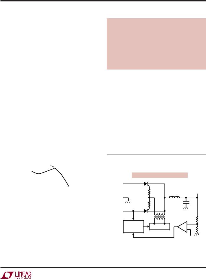
Fully Isolated 2500V Breakdown,
Wideband RMS-to-DC Converter
NOTE: BEFORE PROCEEDING ANY FURTHER, THE READER IS WARNED THAT CAUTION MUST BE USED IN THE CONSTRUCTION, TESTING AND USE OF THIS CIRCUIT. HIGH VOLTAGE, LETHAL POTENTIALS ARE PRESENT IN THIS CIRCUIT. EXTREME CAUTION MUST BE USED IN WORKING WITH, AND MAKING CONNECTIONS TO, THIS CIRCUIT. REPEAT: THIS CIRCUIT CONTAINS DANGEROUS, HIGH VOLTAGE POTENTIALS. USE CAUTION.
Accurate RMS amplitude measurement of SCR chopped AC line related waveforms is a common requirement. This measurement is complicated by the SCR’s fast switching of a sine wave, introducing odd waveshapes with high frequency harmonic content. Figure 5’s conceptual SCRbased AC/DC converter is typical. The SCRs alternately chop the 220VAC line, responding to a loop enforced, phase modulated trigger to maintain a DC output. Figure 6’s waveforms are representative of operation. Trace A is one AC line phase, trace B the SCR cathodes. The SCR’s irregularly shaped waveform contains DC and high frequency harmonic, requiring wideband RMS conversion for measurement. Additionally, for safety and system interface considerations, the measurement must be fully isolated.
3See Appendix B, “AC Measurement and Signal Handling Practice,” for recommendations on RMS voltmeters and other AC measurement related gossip.
DANGER! Lethal Potentials Present—See Text
220VAC |
|
INPUT |
DC |
OUTPUT |
|
NEUTRAL |
|
220VAC |
|
AC LINE SYNC |
|
AND PHASE |
TRIGGER |
MODULATION |
|
|
AN106 F05 |
|
REF |
Figure 5. Conceptual AC/DC Converter is Typical of SCR-Based Configurations. Feedback Directed, AC Line Synchronized Trigger Phase Modulates SCR Turn-On, Controlling DC Output
an106f
AN106-3

Application Note 106
A = 100V/DIV
B = 50V/DIV
ON 170 VDC
LEVEL
1ms/DIV |
AN106 F06 |
|
Figure 6. Typical SCR-Based Converter Waveforms Taken at AC Line (Trace A) and SCR Cathodes (Trace B). SCR’s Irregularly Shaped Waveform Contains DC and High Frequency Harmonic, Requiring Wideband RMS Converter for Measurement
Figure 7 provides isolated power and data output paths to anRMS-to-DCconverter,permittingsafe,wideband,digital output RMS measurement. A pulse generator configured comparator combines with Q1 and Q2 to drive T1, resulting in isolated 5V power at T1’s rectified, filtered and zener regulated output. The RMS-to-DC converter senses either 135VAC or 270VAC full-scale inputs via a resistive divider. The converter’s DC output feeds a self-clocked, serially interfaced A/D converter; optocouplers convey output data across the isolation barrier. The LTC6650 provides a 1V reference to the A/D and biases the RMS-to-DC converter’s inputs to accommodate the voltage divider’s AC swing. Calibration is accomplished by adjusting the 20k trim while noting output data agreement with the input AC voltage. Circuit accuracy is within 1% in a 200kHz bandwidth.
|
PULSE GENERATOR |
POWER |
5V |
|
|
|
|
|
|
|
|
1N4148 |
1k |
DRIVER |
|
|
|
|
|
|
|
|
|
|
|
|
|
|
|
|
||
|
|
|
|
|
|
|
|
|
|
|
|
220k |
|
|
1k |
|
|
|
|
|
|
|
|
|
|
Q2 |
|
ISOLATED POWER SUPPLY |
||||
|
|
|
|
|
|
|||||
|
|
|
|
|
ZTX-749 |
|||||
|
|
|
|
|
|
|
|
|
||
|
– |
|
|
100Ω |
2Ω |
|
1N5817 |
|
|
|
0.001µF |
|
1k |
Q1 |
|
|
|
|
|||
LT1671 |
|
|
|
|
|
|
5V ISO |
|||
|
|
3 |
|
|
|
+ |
||||
|
|
|
2N2369 |
1 |
|
1N4689 |
||||
|
|
|
|
|
|
|||||
|
+ |
|
|
|
1N4148 |
100µF |
||||
|
|
750k |
|
|
6 |
5.1V |
|
|||
|
|
|
4 |
|
|
|||||
|
|
|
|
|
|
|
|
|
||
|
|
|
750k |
|
|
|
|
|
|
|
|
|
|
5V |
|
T1 |
|
|
|
|
|
|
|
|
750k |
|
|
|
|
|
|
|
|
|
|
ISOLATION/POWER |
|
|
|
|
|||
|
|
|
|
TRANSFORMER |
|
|
|
|
||
2500V BREAKDOWN |
DANGER! Lethal Potentials Present—See Text |
ISOLATION BARRIER |
|
DATA |
5V |
4.7k |
|
|
|
|
|
ISOLATORS |
|
5V ISO |
A/D |
|
|
RMS CONVERTER |
|
SCK |
|
5V ISO |
5V ISO |
|
|
CALIBRATE |
|
|
|
|
|
|
|||
|
|
|
|
|
5V ISO |
||
|
|
|
+V |
|
– |
20k |
|
|
|
|
|
|
|
||
|
|
|
|
|
|
0.1µF |
|
|
|
SCK |
VIN |
LT1006 |
|
+V |
|
|
|
|
|
|
|
|
|
DATA |
5V |
|
|
|
|
|
LTC2400 |
+ |
|
|
|
|
|
|
OUT |
IN1 |
|||||
OUTPUTS |
|
|
|
SDO |
|
|
|
|
|
|
|
|
1µF† |
|
|||||||
|
|
|
|
|
|
|
FO |
GND CS REF |
|
|
|
|
|
|
|
LTC1967 |
|||||
|
|
|
|
|
|
|
|
|
|
|
|
|
|
OUT RTN |
IN2 |
||||||
SDO |
|
|
|
|
|
|
|
|
|
|
|
|
|
|
|
|
|
|
|
EN |
GND |
|
|
|
|
|
|
|
|
|
|
|
|
|
|
|
|
|
|
|
|
|
|
|
|
|
|
|
|
|
|
|
|
|
|
|
|
|
|
|
|
|
|
|
|
|
+ |
|
|
|
|
5V ISO |
10µF |
|
|
|
|
|
|
|
|
||
4.7k |
5V ISO |
|
|
|
|
|
|
|
|
||
1µF |
|
|
LT6650 |
1VDC |
|
ISOLATORS = AGILENT-HCPL-2300-010 |
400mV |
+ |
|
||
T1 = BI TECHNOLOGIES HM-41-11510 |
OUT |
AN106 F07 |
|||
REFERENCE |
|||||
|
|||||
* = 1% METAL FILM RESISTOR |
– |
|
|
||
|
|
|
|||
† = WIMA MKS-2 |
|
FB |
15k* |
||
|
|
||||
= CIRCUIT COMMON |
|
|
|
1µF |
|
|
|
|
|
||
= AC LINE GROUND |
|
|
|
10k* |
|
|
|
|
|
182k*
182k*
INPUT 135VAC OR 270VAC FULL SCALE
1k*
Figure 7. Isolated RMS Converter Permits Safe, Digital Output, Wideband RMS Measurement. T1-Based Circuitry Supplies Isolated Power. RMS-to-DC Converter Senses High Voltage Input via Resistive Divider. A/D Converter Provides Digital Output Through Optoisolators. Accuracy is 1% in 200kHz Bandwidth
an106f
AN106-4
Application Note 106
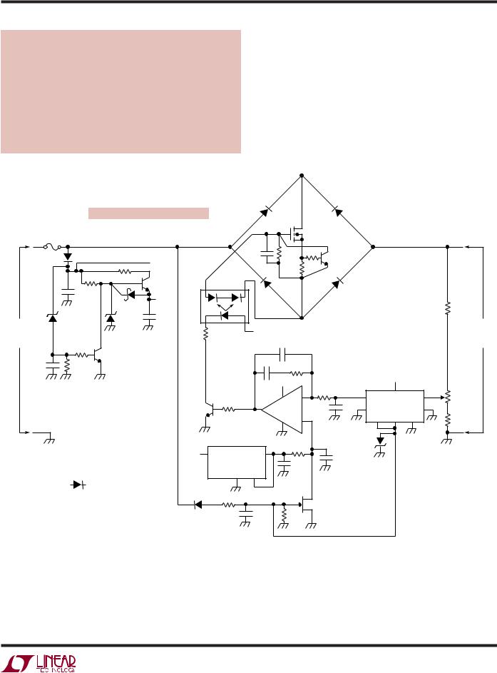
Low Distortion AC Line RMS Voltage Regulator
NOTE: BEFORE PROCEEDING ANY FURTHER, THE READER IS WARNED THAT CAUTION MUST BE USED IN THE CONSTRUCTION, TESTING AND USE OF THIS CIRCUIT. HIGH VOLTAGE, LETHAL POTENTIALS ARE PRESENT IN THIS CIRCUIT. EXTREME CAUTION MUST BE USED IN WORKING WITH, AND MAKING CONNECTIONS TO, THIS CIRCUIT. REPEAT: THIS CIRCUIT CONTAINS DANGEROUS, HIGH VOLTAGE POTENTIALS. USE CAUTION.
Almost all AC line voltage regulators rely on some form of waveform chopping, clipping or interruption to function. This is efficient, but introduces waveform distortion, which is unacceptable in some applications. Figure 8 regulates the AC line’s RMS value within 0.25% over wide input swings and does not introduce distortion. It does this by continuously controlling the conductivity of a series pass MOSFET in the AC lines path. Enclosing the MOSFET in a diode bridge permits it to operate during both AC line polarities.
AC SERIES PASS
AND CURRENT LIMIT
DANGER! Lethal Potentials Present—See Text
AC |
1.5A |
|
|
|
HIGH |
SB |
|
|
|
|
|
|
+V REGULATORS |
|
|
|
|
|
170V |
|
470k |
|
100k |
Q4 |
|
|
|
|
|
|
0.47µF |
|
|
MPSA42 |
|
|
|
|
|
|
|
|
BAT85 |
5V |
|
|
|
|
|
|
1N5281B |
|
1N4690 |
0.1µF |
|
200V |
|
5.6V |
|
UNREGULATED |
|
|
||
|
|
|
|
|
AC LINE |
|
|
|
|
INPUT |
|
|
|
|
|
200k |
Q3 |
OVERVOLTAGE |
|
|
|
|||
0.22µF |
200k |
2N5210 PROTECTION |
||
|
|
|
||
AC
LOW
HEAT SINK IRF-840
*1% METAL FILM RESISTOR OPTODRIVER = TOSHIBA TLP190B
= 1N4005
|
|
|
|
Q2 |
AC HIGH |
|
|
|
|
|
IRF-840 |
|
|
|
0.03µF |
430k |
10k |
Q6 |
|
|
|
|
0.7Ω |
|
2N3904 |
|
|
|
|
|
|
|
||
|
|
|
|
|
2.2M* |
|
10k |
170V |
|
|
|
FEEDBACK |
VAC |
|
|
|
SENSE |
REGULATED |
||
2W |
|
|
|
|
||
ISOLATED |
0.1µF |
CONTROL |
|
OUTPUT |
||
|
GATE BIAS |
AMPLIFIER |
|
|
||
|
|
|
|
|||
|
1µF |
|
22k |
|
RMS-TO-DC CONVERTER |
|
|
|
|
|
|
||
|
|
|
|
5V |
|
C1 |
5V |
|
|
|
|
|
|
|
|
|
|
|
105VAC |
||
|
|
|
|
10k |
|
|
|
1k |
||
|
|
|
|
|
|
+V |
|
|||
|
|
|
|
|
|
|
TO 120VAC |
|||
|
|
|
|
– |
|
OUT |
IN1 |
|
||
|
|
5.6k |
|
|
LTC1966 |
|
ADJUST |
|||
Q1 |
|
|
A1 |
1µF |
|
IN2 |
|
|||
|
|
|
OUT RTN |
|
|
|||||
2N3440 |
|
|
|
LT1077 |
|
|
|
|||
|
|
|
|
EN |
–V |
GND |
|
|
||
|
|
|
|
+ |
|
|
7.32k* |
|||
|
|
|
|
|
|
|
|
|
||
|
|
|
|
|
|
|
|
|
|
|
|
|
REFERENCE |
|
|
1N4689 |
|
|
|
|
|
5V |
IN |
0.4V OUT |
330k |
2.2µF |
5.1V |
|
|
AC LOW |
||
|
|
|
|
|||||||
|
|
|
|
|
|
|||||
|
|
LT6650 |
|
1µF |
MYLAR |
|
|
|
|
|
|
|
GND |
FB |
|
|
|
|
|
|
|
|
|
1M |
|
Q5 |
|
|
|
|
|
|
|
|
|
|
|
|
|
|
|
|
|
|
|
|
0.22µF |
2N4393 |
|
|
|
|
|
|
|
|
|
100k |
|
|
|
|
|
|
|
|
|
|
|
|
|
|
AN106 F08 |
|
|
|
|
|
|
SOFT-START/–VBIAS |
|
|
|
|
|
|
|
Figure 8. Adjustable AC Line Voltage Regulator Introduces No Waveform Distortion. Line Voltage RMS Value is Sensed and Compared to a Reference by A1. A1 Biases Photovoltaic Optocoupler via Q1, Setting Q2-Diode Bridge Conductivity and Closing a Control Loop. VIN Must be ≥2V Above VOUT to Maintain Regulation
an106f
AN106-5

Application Note 106
The AC line voltage is applied to the Q2-diode bridge. The Q2-diode bridge output is sensed by a calibrated variable voltage divider which feeds C1. C1’s output, representing the regulated lines RMS value, is routed to control amplifier A1 and compared to a reference. A1’s output biases Q1, controlling drive to a photovoltaic optoisolator. The optoisolator’s output voltage provides level-shifted bias to diode bridge enclosed Q2, closing a control loop which regulates the output’s RMS voltage against AC line and load shifts. RC components in A1’s local feedback path stabilize the control loop. The loop operates Q2 in its linear region, much like a common low voltage DC linear regulator. The result is absence of introduced distortion at the expense of lost power. Available output power is constrained by heat dissipation. For example, with the output adjustment set to regulate 10V below the normal input, Q2 dissipates about 10W at 100W output. This figure can be improved upon. The circuit regulates for VIN ≥ 2V above VOUT, but operation in this region risks regulation dropout as VIN varies.
CircuitdetailsincludeJFETQ5andassociatedcomponents. The passive components associated with Q5’s gate form a slow turn-on negative supply for C1. They also provide gate bias for Q5. Q5, a soft-start, prevents abrupt AC power application to the output at start-up. When power is off, Q5 conducts, holding A1’s “+” input low. When power is applied, A1 initially has a zero volt reference, causing the control loop to set the output at zero. As the 1MΩ 0.22µF combination charges, Q5’s gate moves negative, causing its channel conductivity to gradually decay. Q5 ramps off, A1’s positive input moves smoothly towards the LT6650’s 400mV reference, and the AC output similarly ascends towards its regulation point. Current sensor Q6, measuring across the 0.7Ω shunt, limits output current to about 1A. At normal line inputs (90VAC to 135VAC) Q4 supplies 5V operating bias to the circuit. If line voltage rises beyond this point, Q3 comes on, turning off Q4 and shutting down the circuit.
X1000 DC Stabilized Millivolt Preamplifier
The preceding circuits furnish high level inputs to the RMS converter. Many applications lack this advantage and some formofpreamplifierisrequired.Highgainpre-amplification for the RMS converter requires more attention than might be supposed. The preamplifier must have low offset error because the RMS converter (desirably) processes DC as
legitimate input. More subtly, the preamplifier must have far more bandwidth than is immediately apparent. The amplifiers –3db bandwidth is of interest, but its closed loop 1% amplitude error bandwidth must be high enough to maintain accuracy over the RMS converter’s 1% error passband. This is not trivial, as very high open-loop gain at the maximum frequency of interest is required to avoid inaccurate closed-loop gain.
Figure 9 shows an x1000 preamplifier which preserves the LTC1966’s DC-6kHz 1% accuracy. The amplifier may be either AC or DC coupled to the RMS converter. The 1mV full-scale input is split into high and low frequency paths. AC coupled A1 and A2 take a cascaded, high frequency gain of 1000. DC coupled, chopper stabilized A3 also has X1000 gain, but is restricted to DC and low frequency by its RC input filter. Assuming the switch is set to “DC + AC,” high and low frequency path information recombine at the RMS converter. The high frequency paths 650kHz –3db responsecombineswiththelowfrequencysectionsmicrovolt level offset to preserve the RMS converters DC-6kHz 1% error. If only AC response is desired, the switch is set to the appropriate position. The minimum processable input, set by the circuits noise floor, is 15µV.
Wideband Decade Ranged X1000 Preamplifier
The LTC1968, with a 500kHz, 1% error bandwidth, poses a significant challenge for an accurate preamplifier, but Figure 10 meets the requirement. This design features decade ranged gain to X1000 with a 1% error bandwidth beyond 500kHz, preserving the RMS converters 1% error bandwidth. Its 20µV noise floor maintains wideband performance at microvolt level inputs.
Q1A and Q1B form a low noise buffer, permitting high impedance inputs. A1 and A2, both gain switchable, take cascaded gain in accordance with the figure’s table. The gains are settable via reed relays controlled by a 2-bit code. A2’s output feeds the RMS converter and the converter’s output is smoothed by a Sallen-Keys active filter. The circuit maintains 1% error over a 10Hz to 500kHz bandwidth at all gains due to the preamplifiers –3db, 10MHz bandwidth. The 10Hz low frequency restriction could be eliminated with a DC stabilization path similar to Figure 9’s but its gain would have to be switched in concert with the A1-A2 path.
an106f
AN106-6
 Loading...