


Linear Technology LT1008S8, LT1008MH, LT1008IN8, LT1008CN8, LT1008CJ8 Datasheet
...FEATURES
■Guaranteed Bias Current
TA = 25°C: 100pA Max
TA = – 55°C to 125°C: 600pA Max
■Guaranteed Offset Voltage: 120 V Max
■Guaranteed Drift: 1.5 V/°C Max
■Low Noise, 0.1Hz to 10Hz: 0.5 VP-P
■Guaranteed Low Supply Current: 600 A Max
■Guaranteed CMRR: 114dB Min
■Guaranteed PSRR: 114dB Min
■Guaranteed Voltage Gain with 5mA Load Current
APPLICATIOUS
■Precision Instrumentation
■Charge Integrators
■Wide Dynamic Range Logarithmic Amplifiers
■Light Meters
■Low Frequency Active Filters
■Standard Cell Buffers
■Thermocouple Amplifiers
LT1008
Picoamp Input Current,
Microvolt Offset,
Low Noise Op Amp
DESCRIPTIOU
The LT®1008 is a universal precision operational amplifier that can be used in practically all precision applications. The LT1008 combines for the first time, picoampere bias currents (which are maintained over the full – 55°C to 125°C temperature range), microvolt offset voltage (and low drift with time and temperature), low voltage and current noise, and low power dissipation. Extremely high common mode and power supply rejection ratios, and the ability to deliver 5mA load current with high voltage gain round out the LT1008’s superb precision specifications.
The all around excellence of the LT1008 eliminates the necessity of the time consuming error analysis procedure of precision system design in many applications; the LT1008 can be stocked as the universal precision op amp.
The LT1008 is externally compensated with a single capacitor for additional flexibility in shaping the frequency response of the amplifier. It plugs into and upgrades all standard LM108A/LM308A applications. For an internally compensated version with even lower offset voltage but otherwise similar performance see the LT1012.
 , LTC and LT are registered trademarks of Linear Technology Corporation.
TYPICAL APPLICATIOU
Input Amplifier for 4.5 Digit Voltmeter Input Bias Current vs Temperature
|
|
|
|
|
|
|
|
|
|
|
|
100 |
|
|
|
|
|
|
1000pF |
|
|
|
|
|
|
|
|
|
|
|
|
1 |
15V |
|
|
|
|
|
(pA) |
50 |
|
|
|
2 |
|
|
|
|
|
|
|
|
|||
|
|
|
|
|
|
0.1V |
|
|
|
|
|||
|
|
– |
|
8 |
|
|
|
|
|
|
|||
INPUT |
|
|
|
|
|
|
CURRENT |
|
|
||||
|
|
|
7 |
|
|
1V |
|
|
|
|
|||
0.1V |
100k |
|
|
|
6 |
|
|
|
0 |
|
|||
|
|
|
LT1008 |
|
|
|
|
|
|
|
|||
1V |
5% |
3 |
+ |
|
|
|
9k* |
10V |
|
|
|
|
|
|
|
|
|
4 |
|
|
|
|
BIAS |
|
|
||
9M |
|
|
|
|
|
100V |
|
|
–50 |
|
|||
|
|
|
|
–15V |
|
|
|
|
|
||||
|
|
|
|
|
|
|
|
|
|
|
|||
|
|
|
|
|
|
1000V |
|
|
INPUT |
|
|
||
10V |
|
|
|
|
|
1k* |
TO 1V FULL-SCALE |
|
|
||||
|
|
|
|
|
|
|
|
||||||
|
|
|
|
|
|
|
ANALOG-TO-DIGITAL |
|
|
||||
|
|
|
|
|
|
|
|
|
–100 |
|
|||
900k |
|
|
|
|
|
|
|
|
CONVERTER |
|
|
||
|
|
|
|
|
|
|
|
|
|
|
|||
100V |
|
|
|
|
|
|
*RATIO MATCH ±0.01% |
|
|
|
|
||
90k |
|
|
|
|
|
|
|
|
–150 |
|
|||
|
|
|
|
|
|
|
|
|
|
|
–25 |
||
1000V |
|
|
|
|
|
|
|
|
|
|
|
–50 |
|
|
|
|
|
|
|
THIS APPLICATION REQUIRES LOW |
|
|
|
||||
|
FN507 |
|
|
|
|
|
|
|
|
||||
10k |
|
|
|
|
|
BIAS CURRENT AND OFFSET VOLTAGE, |
|
|
|
||||
|
ALLEN BRADLEY |
|
|
LOW NOISE AND LOW DRIFT WITH |
|
|
|
||||||
|
DECADE VOLTAGE DIVIDER |
|
TIME AND TEMPERATURE |
1008 TA01 |
|
|
|
||||||
UNDERCANCELLED UNIT
OVERCANCELLED UNIT
0 |
25 |
50 |
75 |
100 |
125 |
TEMPERATURE (°C)
1008 TA02
1
LT1008
ABSOLUTE
WAXIWUW
RATIUGS (Note 1)
Supply Voltage ...................................................... |
±20V |
Operating Temperature Range |
|
|
.....................Differential Input Current (Note 2) |
±10mA |
|
LT1008M (OBSOLETE) ............... |
– 55°C to 125°C |
Input Voltage ........................................................ |
±20V |
|
LT1008C ................................................. |
0°C to 70°C |
Output Short-Circuit Duration ......................... |
Indefinite |
|
LT1008I ............................................. |
– 40°C to 85°C |
Storage Temperature Range ................. |
– 65°C to 150°C |
Lead Temperature (Soldering, 10 sec).................. |
300°C |
|
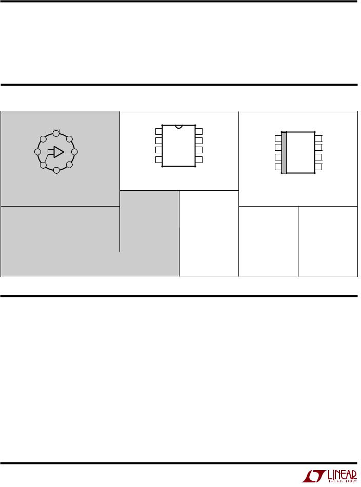
PACKAGE/ORDER IUFORWATIOU |
|
|
|
|
|
|
|||||||
|
TOP VIEW |
|
|
|
|
|
TOP VIEW |
|
|
|
|
|
|
|
COMP2 |
|
|
|
COMP1 |
1 |
8 |
COMP2 |
|
|
TOP VIEW |
|
|
|
8 |
|
V+ |
|
|
|
|
|
|||||
|
7 |
|
|
|
|
|
+ |
COMP1 |
1 |
8 |
COMP2 |
||
COMP1 |
1 |
|
–IN |
2 |
7 |
V |
|||||||
|
|
|
|
|
|
|
|
|
V+ |
||||
–IN 2 |
– |
|
6 |
OUT |
+IN |
3 |
6 |
OUT |
–IN |
2 |
7 |
||
+ |
|
V– |
|
|
|
|
+IN |
3 |
6 |
OUT |
|||
+IN |
3 |
5 |
NC |
4 |
5 |
NC |
|||||||
|
|
|
|
|
V– |
4 |
5 |
NC |
|||||
|
4 |
|
|
|
|
|
N8 PACKAGE |
|
|
|
|
|
|
|
V– (CASE) |
|
|
|
|
|
|
|
|
|
|
|
|
|
|
|
|
|
|
8-LEAD PDIP |
|
|
|
|
S8 PACKAGE |
|
|
|
H PACKAGE |
|
|
|
TJMAX = 150°C, θJA = 130°C/W |
|
|
8-LEAD PLASTIC SO |
|
||||
8-LEAD TO-5 METAL CAN |
|
|
|
|
|
TJMAX = 150°C, θJA = 190°C/W |
|
||||||
TJMAX = 150°C, θJA = 150°C/W, θJC |
= 45°C/W |
J8 PACKAGE 8-LEAD CERDIP |
|
|
|
||||||||
|
|
|
|
|
|
||||||||
TJMAX = 150°C, θJA = 100°C/W |
|
|
|
|
|
|
|||||||
|
|
|
|
|
|
|
|
|
|
|
|||
ORDER PART |
ORDER PART |
ORDER PART |
ORDER PART |
S8 PART |
NUMBER |
NUMBER |
NUMBER |
NUMBER |
MARKING |
LT1008MH |
LT1008MJ8 |
LT1008CN8 |
LT1008S8 |
1008 |
LT1008CH |
LT1008CJ8 |
LT1008IN8 |
|
|
OBSOLETE PACKAGES
Consider N8 or S8 Package for Alternate Source
Consult LTC Marketing for parts specified with wider operating temperature ranges.
ELECTRICAL CHARACTERISTICS VS = ±15V, VCM = 0V, TA = 25°C, unless otherwise noted.
|
|
|
LT1008M/I |
|
LT1008C |
|
|
|
||
SYMBOL |
PARAMETER |
CONDITIONS |
MIN |
TYP |
MAX |
MIN |
TYP |
MAX |
UNITS |
|
|
|
|
|
|
|
|
|
|
|
|
VOS |
Input Offset Voltage |
|
|
30 |
120 |
|
30 |
120 |
V |
|
|
|
(Note 3) |
|
40 |
180 |
|
40 |
180 |
V |
|
|
Long-Term Input Offset Voltage Stability |
|
|
0.3 |
|
|
0.3 |
|
V/Month |
|
|
|
|
|
|
|
|
|
|
|
|
IOS |
Input Offset Current |
|
|
30 |
100 |
|
30 |
100 |
pA |
|
|
|
(Note 4) |
|
40 |
150 |
|
40 |
150 |
pA |
|
IB |
Input Bias Current |
|
|
±30 |
±100 |
|
±30 |
±100 |
pA |
|
|
|
(Note 5) |
|
±40 |
±150 |
|
±40 |
±150 |
pA |
|
en |
Input Noise Voltage |
0.1Hz to 10Hz |
|
0.5 |
|
|
0.5 |
|
VP-P |
|
|
Input Noise Voltage Density |
fO = 10Hz (Note 4) |
|
17 |
30 |
|
17 |
30 |
nV√ |
|
|
|
|
Hz |
|||||||
|
|
fO = 1000Hz (Note 5) |
|
14 |
22 |
|
14 |
22 |
nV/√Hz |
|
in |
Input Noise Current Density |
fO = 10Hz |
|
20 |
|
|
20 |
|
fA/√ |
|
|
|
|
|
Hz |
||||||
AVOL |
Large-Signal Voltage Gain |
VOUT = ±12V, RL ≥ 10k |
200 |
2000 |
|
200 |
2000 |
|
V/mV |
|
|
|
VOUT = ±10V, RL ≥ 2k |
120 |
600 |
|
120 |
600 |
|
V/mV |
|
2

LT1008
ELECTRICAL CHARACTERISTICS VS = ±15V, VCM = 0V, TA = 25°C, unless otherwise noted.
|
|
|
LT1008M/I |
LT1008C |
|
|
|||
SYMBOL |
PARAMETER |
CONDITIONS |
MIN |
TYP |
MAX |
MIN |
TYP |
MAX |
UNITS |
|
|
|
|
|
|
|
|
|
|
CMRR |
Common Mode Rejection Ratio |
VCM = ±13.5V |
114 |
132 |
|
114 |
132 |
|
dB |
PSRR |
Power Supply Rejection Ratio |
VS = ±2V to ±20V |
114 |
132 |
|
114 |
132 |
|
dB |
|
Input Voltage Range |
|
±13.5 |
±14 |
|
±13.5 |
±14 |
|
V |
|
|
|
|
|
|
|
|
|
|
VOUT |
Output Voltage Swing |
RL = 10k |
±13 |
±14 |
|
±13 |
±14 |
|
V |
|
Slew Rate |
CF = 30pF |
0.1 |
0.2 |
|
0.1 |
0.2 |
|
V/ s |
IS |
Supply Current |
(Note 3) |
|
380 |
600 |
|
380 |
600 |
A |
The ● indicates specifications which apply over the full operating temperature range of – 55°C ≤ TA ≤ 125°C for the LT1008M, |
–40°C |
||||||||||||
≤ TA ≤ 85°C for the LT1008I and 0°C ≤ TA ≤ 70°C for the LT1008C. VS = ±15V, VCM = 0V, unless otherwise noted. |
|
|
|
|
|
|
|||||||
|
|
|
|
LT1008M/I |
LT1008C |
|
|
|
|
||||
SYMBOL |
PARAMETER |
CONDITIONS |
|
MIN |
TYP |
MAX |
MIN |
TYP |
MAX |
UNITS |
|||
|
|
|
|
|
|
|
|
|
|
|
|
|
|
VOS |
Input Offset Voltage |
|
● |
|
50 |
250 |
|
40 |
180 |
V |
|||
|
|
(Note 3) |
● |
|
60 |
320 |
|
50 |
250 |
V |
|
||
|
Average Temperature Coefficient of |
|
|
|
|
|
|
|
|
V/°C |
|||
|
Input Offset Voltage |
|
● |
|
0.2 |
1.5 |
|
0.2 |
1.5 |
||||
|
|
|
|
|
|
|
|
|
|
|
|
|
|
IOS |
Input Offset Current |
|
● |
|
60 |
250 |
|
40 |
180 |
pA |
|||
|
|
(Note 3) |
● |
|
80 |
350 |
|
50 |
250 |
pA |
|||
|
Average Temperature Coefficient of |
|
|
|
0.4 |
2.5 |
|
0.4 |
2.5 |
pA/°C |
|
||
|
Input Offset Current |
|
● |
|
|
||||||||
|
|
|
|
|
|
|
|
|
|
|
|
|
|
IB |
Input Bias Current |
|
● |
|
±80 |
±600 |
|
±40 |
±180 |
pA |
|||
|
|
(Note 3) |
● |
|
±150 |
±800 |
|
±50 |
±250 |
pA |
|||
|
Average Temperature Coefficient of |
|
|
|
|
|
|
|
|
pA/°C |
|
||
|
Input Bias Current |
|
● |
|
0.6 |
6 |
|
0.4 |
2.5 |
||||
|
|
|
|
|
|
|
|
|
|
|
|
|
|
AVOL |
Large-Signal Voltage Gain |
VOUT = ±12V, RL ≥ 10k |
● |
100 |
1000 |
|
150 |
1500 |
|
V/mV |
|
||
CMRR |
Common Mode Rejection Ratio |
VCM = ±13.5V |
● |
108 |
128 |
|
110 |
130 |
|
dB |
|
||
PSRR |
Power Supply Rejection Ratio |
VS = ±2.5V to ±20V |
● |
108 |
126 |
|
110 |
128 |
|
dB |
|||
|
Input Voltage Range |
|
● |
±13.5 |
|
|
±13.5 |
|
|
|
V |
|
|
|
|
|
|
|
|
|
|
|
|
|
|
|
|
VOUT |
Output Voltage Swing |
RL = 10k |
● |
±13 |
±14 |
|
±13 |
±14 |
|
|
V |
|
|
IS |
Supply Current |
|
● |
|
400 |
800 |
|
400 |
800 |
A |
|||
(LT1008S8 only) VS = ±15V, VCM = 0V, TA = 25°C, unless otherwise noted. |
|
|
|
|
|
|
|
|
|
|
|
||
|
|
|
|
|
|
|
|
|
|
|
|
||
SYMBOL |
PARAMETER |
CONDITIONS |
|
|
|
MIN |
TYP |
MAX |
UNITS |
||||
|
|
|
|
|
|
|
|
|
|
|
|
|
|
VOS |
Input Offset Voltage |
|
|
|
|
|
30 |
|
200 |
V |
|||
|
|
(Note 3) |
|
|
|
|
40 |
|
250 |
V |
|||
|
Long-Term Input Offset Voltage Stability |
|
|
|
|
|
0.3 |
|
V/Month |
||||
|
|
|
|
|
|
|
|
|
|
|
|||
IOS |
Input Offset Current |
|
|
|
|
|
100 |
280 |
pA |
||||
|
|
(Note 3) |
|
|
|
|
120 |
380 |
pA |
||||
IB |
Input Bias Current |
|
|
|
|
|
±100 |
±300 |
pA |
||||
|
|
(Note 3) |
|
|
|
|
±120 |
±400 |
pA |
||||
en |
Input Noise Voltage |
0.1Hz to 10Hz |
|
|
|
|
0.5 |
|
VP-P |
|
|||
|
Input Noise Voltage Density |
fO = 10Hz (Note 5) |
|
|
|
|
17 |
|
30 |
nV/√ |
|
|
|
|
|
|
|
|
|
Hz |
|||||||
|
|
fO = 1000Hz (Note 5) |
|
|
|
|
14 |
|
22 |
nV/√ |
Hz |
|
|
3

LT1008
ELECTRICAL CHARACTERISTICS (LT1008S8 only) VS = ±15V, VCM = 0V, TA = 25°C, unless otherwise noted.
SYMBOL |
PARAMETER |
CONDITIONS |
MIN |
TYP |
MAX |
UNITS |
|
|
|
|
|
|
|
|
|
in |
Input Noise Current Density |
fO = 10Hz |
|
20 |
|
fA/√ |
|
|
|
Hz |
|||||
AVOL |
Large-Signal Voltage Gain |
VOUT = ±12V, RL ≥ 10k |
200 |
2000 |
|
V/mV |
|
|
|
VOUT = ±10V, RL ≥ 2k |
120 |
600 |
|
V/mV |
|
CMRR |
Common Mode Rejection Ratio |
VCM = ±13.5V |
110 |
132 |
|
|
dB |
PSRR |
Power Supply Rejection Ratio |
VS = ±2V to ±20V |
110 |
132 |
|
|
dB |
|
Input Voltage Range |
|
±13.5 |
±14 |
|
|
V |
|
|
|
|
|
|
|
|
VOUT |
Output Voltage Swing |
RL = 10k |
±13 |
±14 |
|
|
V |
|
Slew Rate |
CF = 30pF |
0.1 |
0.2 |
|
V/ s |
|
IS |
Supply Current |
(Note 3) |
|
380 |
600 |
|
A |
(LT1008S8 only) The ● indicates specifications which apply over the full operating temperature range of 0°C ≤ TA ≤ 70°C. VS = ±15V, VCM = 0V, unless otherwise noted.
SYMBOL |
PARAMETER |
CONDITIONS |
|
MIN |
TYP |
MAX |
UNITS |
|
|
|
|
|
|
|
|
VOS |
Input Offset Voltage |
|
● |
|
40 |
280 |
V |
|
|
(Note 3) |
● |
|
50 |
340 |
V |
|
Average Temperature Coefficient of |
|
● |
|
0.2 |
1.8 |
V/°C |
|
Input Offset Voltage |
|
|
|
|
|
|
|
|
|
|
|
|
|
|
IOS |
Input Offset Current |
|
● |
|
120 |
380 |
pA |
|
|
(Note 3) |
● |
|
140 |
500 |
pA |
|
Average Temperature Coefficient of |
|
● |
|
0.4 |
4 |
pA/°C |
|
Input Offset Current |
|
|
|
|
|
|
|
|
|
|
|
|
|
|
IB |
Input Bias Current |
|
● |
|
±120 |
±420 |
pA |
|
|
(Note 3) |
● |
|
±140 |
±550 |
pA |
|
Average Temperature Coefficient of |
|
● |
|
0.4 |
5 |
pA/°C |
|
Input Bias Current |
|
|
|
|
|
|
|
|
|
|
|
|
|
|
AVOL |
Large-Signal Voltage Gain |
VOUT = ±12V, RL ≥ 10k |
● |
150 |
1500 |
|
V/mV |
CMRR |
Common Mode Rejection Ratio |
VCM = ±13.5V |
● |
108 |
130 |
|
dB |
PSRR |
Power Supply Rejection Ratio |
VS = ±2.5V to ±20V |
● |
108 |
128 |
|
dB |
|
Input Voltage Range |
|
● |
±13.5 |
|
|
V |
|
|
|
|
|
|
|
|
VOUT |
Output Voltage Swing |
RL = 10k |
● |
±13 |
±14 |
|
V |
IS |
Supply Current |
|
● |
|
400 |
800 |
A |
Note 1: Absolute Maximum Ratings are those values beyond which the life of a device may be impaired.
Note 2: Differential input voltages greater than 1V will cause excessive current to flow through the input protection diodes unless current limiting resistors are used.
Note 3: These specifications apply for ±2V ≤ VS ≤ ±20V (±2.5V ≤ VS ≤ ±20V over the temperature range) and
–13.5V ≤ VCM ≤ 13.5V (for VS = ±15V).
Note 4: 10Hz noise voltage density is sample tested on every lot. Devices 100% tested at 10Hz are available on request.
Note 5: This parameter is tested on a sample basis only.
4

|
|
|
|
|
|
|
|
|
LT1008 |
FREQUEUCY COWPEUSATIOU CIRCUITS |
|
|
|
|
|||||
|
Standard Compensation Circuit |
Alternate* Frequency Compensation |
|||||||
R1 |
|
R2 |
|
|
|
R1 |
|
R2 |
|
–VIN |
|
|
|
|
–VIN |
|
|
|
*IMPROVES REJECTION OF POWER |
|
|
|
|
**BANDWIDTH AND SLEW RATE |
|
|
|
SUPPLY NOISE BY A FACTOR OF 5 |
|
|
|
|
|
|
|
|
**BANDWIDTH AND SLEW RATE ARE |
||
|
2 |
– |
|
ARE PROPORTIONAL TO 1/CF |
2 |
– |
|
||
|
6 |
6 |
PROPORTIONAL TO 1/CS |
||||||
|
|
LT1008 |
VOUT |
|
|
|
VOUT |
||
R3 |
3 |
8 |
|
3 |
|
LT1008 |
|||
+ |
|
|
+ |
|
|
||||
+VIN |
|
CF ≥ |
R1CO |
+VIN |
|
8 |
|
||
|
|
1 |
R1 + R2 |
|
|
|
CS** |
|
|
|
|
|
CO = 30pF |
|
|
|
100pF |
|
|
|
|
CF** |
|
1008 FCC01 |
|
|
|
|
1008 FCC02 |
|
|
|
|
|
|
|
|
||
|
|
|
|
FOR |
R2 > 200, NO EXTERNAL FREQUENCY COMPENSATION IS NECESSARY |
|
|||
|
|
|
|
|
R1 |
|
|
|
|
TYPICAL PERFORWAUCE CHARACTERISTICS
OFFSET VOLTAGE DRIFT WITH TEMPERATURE ( V/°C)
Offset Voltage Drift vs Source |
|
Offset Voltage vs Source |
|
|
|
|
|
|
|
|
|
|||||||
Resistance (Balanced or |
|
|
Resistance (Balanced or |
|
|
Input Bias Current vs |
|
|
|
|||||||||
Unbalanced) |
|
|
|
Unbalanced) |
|
|
|
Common Mode Range |
|
|
|
|||||||
100 |
|
|
|
|
|
10 |
|
|
|
|
|
60 |
|
|
|
|
|
|
|
|
|
|
|
|
VS = ±15V |
|
|
|
|
VS = ±15V |
|
|
|
|
|
||
|
|
|
|
|
|
TA = 25°C |
|
|
|
|
TA = 25°C |
|
|
|
|
|
||
|
|
|
|
|
OFFSETINPUTVOLTAGE (mV) |
|
|
|
|
|
|
40 |
DEVICE WITH POSITIVE INPUT CURRENT |
|
||||
|
|
|
|
|
|
|
|
|
|
|
BIASINPUTCURRENT (pA) |
|
||||||
10 |
|
|
|
|
1 |
TYPICAL |
|
|
|
|
|
|
VCM |
|
+ |
|
||
|
|
|
|
|
|
|
|
|
|
20 |
|
|
|
|
|
|
||
|
|
|
|
|
|
|
|
|
|
|
|
|
|
|
RINCM = 2 × 10¹²Ω |
|
||
|
MAXIMUM |
|
|
|
|
|
|
|
|
|
|
0 |
DEVICE WITH NEGATIVE INPUT CURRENT |
|
||||
|
|
|
|
|
|
|
|
|
|
|
|
|
||||||
|
|
|
|
|
|
MAXIMUM |
|
|
|
|
|
|
|
|
|
|
|
|
1 |
|
|
|
|
|
0.1 |
|
|
|
|
–20 |
|
|
|
|
|
|
|
|
|
|
|
|
|
|
|
|
|
|
|
|
|
– |
|
|||
|
|
|
|
|
|
|
|
|
|
|
|
|
|
|
|
IB |
|
|
|
|
|
|
|
|
|
|
|
|
|
|
|
|
|
|
|
|
|
|
TYPICAL |
|
|
|
|
|
|
|
|
|
|
–40 |
|
|
|
|
|
|
|
|
|
|
|
|
|
|
|
|
|
|
|
|
|
|
|
|
|
0.1 |
10k |
100k |
1M |
10M |
100M |
0.01 |
10k |
100k |
1M |
10M |
100M |
–60 |
–10 |
– 5 |
0 |
5 |
10 |
15 |
1k |
1k |
–15 |
||||||||||||||||
|
SOURCE RESISTANCE (Ω) |
|
|
SOURCE RESISTANCE (Ω) |
|
|
COMMON MODE INPUT VOLTAGE (V) |
|
||||||||||
1008 G01 |
1008 G02 |
1008 G03 |
CHANGE IN OFFSET VOLTAGE ( V)
Warm-Up Drift
5
VS = ±15V
TA = 25°C
4
3 |
|
|
|
|
|
|
|
|
|
|
|
|
|
|
|
|
|
|
|
|
|
|
|
|
|
2 |
|
|
|
|
|
|
|
|
|
|
|
|
|
|
|
METAL CAN (H) PACKAGE |
|
|
|
||||||
|
|
|
|
|
|
|||||||
|
|
|
|
|
|
|
||||||
|
|
|
|
|
|
|
|
|
|
|
||
|
|
|
|
DUAL-IN-LINE PACKAGE |
|
|
||||||
1 |
|
|
PLASTIC (N) OR CERDIP (J) |
|
|
|||||||
|
|
|
|
|||||||||
0 |
|
|
|
|
|
|
|
|
|
|
|
|
|
|
|
|
|
|
|
|
|
|
|
|
|
|
1 |
2 |
3 |
4 |
|
5 |
||||||
0 |
|
|||||||||||
TIME AFTER POWER ON (MINUTES)
1008 G04
CHANGE IN OFFSET VOLTAGE ( V)
|
|
|
|
|
|
|
|
|
|
|
Offset Voltage Drift with |
|
|
|
|
||||||||||
Long-Term Stability of Four |
|
|
|
Temperature of Four |
|
|
|
|
|
|
|||||||||||||||
Representative Units |
|
|
|
|
|
Representative Units |
|
|
|
|
|
|
|||||||||||||
10 |
|
|
|
|
|
|
|
|
|
|
60 |
|
|
|
|
|
|
|
|
|
|
|
|
|
|
|
|
|
|
|
|
|
|
|
|
|
|
|
|
|
|
|
|
|
|
|
|
|
|
||
8 |
|
|
|
|
|
|
|
|
|
|
40 |
|
|
|
|
|
|
|
|
|
|
|
|
|
|
|
|
|
|
|
|
|
|
|
|
|
|
|
|
|
|
|
|
|
|
|
|
|
|
||
6 |
|
|
|
|
|
|
|
|
|
V)( |
|
|
|
|
|
|
|
|
|
|
|
|
|
|
|
|
|
|
|
|
|
|
|
|
|
|
|
|
|
|
|
|
|
|
|
|
|
|
|||
|
|
|
|
|
|
|
|
|
|
|
|
|
|
|
|
|
|
|
|
|
|
|
|
||
4 |
|
|
|
|
|
|
|
|
|
20 |
|
|
|
|
|
|
|
|
|
|
|
|
|
|
|
|
|
|
|
|
|
|
|
|
VOLTAGE |
|
|
|
|
|
|
|
|
|
|
|
|
|
|
||
2 |
|
|
|
|
|
|
|
|
|
|
|
|
|
|
|
|
|
|
|
|
|
|
|
||
|
|
|
|
|
|
|
|
|
|
|
|
|
|
|
|
|
|
|
|
|
|
|
|
||
|
|
|
|
|
|
|
|
|
|
|
|
|
|
|
|
|
|
|
|
|
|
|
|
|
|
0 |
|
|
|
|
|
|
|
|
|
OFFSET |
0 |
|
|
|
|
|
|
|
|
|
|
|
|
|
|
|
|
|
|
|
|
|
|
|
|
|
|
|
|
|
|
|
|
|
|
|
|
|
|||
–2 |
|
|
|
|
|
|
|
|
|
–20 |
|
|
|
|
|
|
|
|
|
|
|
|
|
|
|
|
|
|
|
|
|
|
|
|
|
|
|
|
|
|
|
|
|
|
|
|
|
|
|
||
–4 |
|
|
|
|
|
|
|
|
|
|
|
|
|
|
|
|
|
|
|
|
|
|
|
|
|
|
|
|
|
|
|
|
|
|
|
|
|
|
|
|
|
|
|
|
|
|
|
|
|
||
|
|
|
|
|
|
|
|
|
|
|
|
|
|
|
|
|
|
|
|
|
|
|
|
|
|
–6 |
|
|
|
|
|
|
|
|
|
|
–40 |
|
|
|
|
|
|
|
|
|
|
|
|
|
|
|
|
|
|
|
|
|
|
|
|
|
|
|
|
|
|
|
|
|
|
|
|
|
|
||
–8 |
|
|
|
|
|
|
|
|
|
|
|
|
|
|
|
|
|
|
|
|
|
|
|
|
|
|
|
|
|
|
|
|
|
|
|
–60 |
|
|
|
|
|
|
|
|
|
|
|
|
|
|
|
|
|
|
|
|
|
|
|
|
|
|
|
|
|
|
|
|
|
|
|
|
|
|
|
||
–10 |
|
|
|
|
|
|
|
|
|
|
|
|
|
|
|
|
|
|
|
|
|
|
|
|
|
|
1 |
2 |
3 |
4 |
5 |
|
|
–25 |
0 |
25 |
50 |
75 |
100 |
125 |
|||||||||||
0 |
|
–50 |
|||||||||||||||||||||||
|
|
|
TIME (MONTHS) |
|
|
|
|
|
|
|
|
|
|
TEMPERATURE (°C) |
|
|
|
|
|||||||
|
|
|
|
|
|
|
|
1008 G05 |
|
|
|
|
|
|
|
|
|
|
|
|
|
1008 G06 |
|||
5
 Loading...