


Linear Technology LTC1177ISW-5, LTC1177ISW-12, LTC1177CSW-5, LTC1177CSW-12, LTC1177CN-12 Datasheet
...
LTC1177-5/LTC1177-12
Isolated MOSFET Drivers
FEATURES
■UL Recognized ®
File E151738 to UL1577
■No Secondary Power Supply
■Drives Any Logic Level FET
■Low Input Current: 1mA Typ (LTC1177-5), 2.5mA Typ (LTC1177-12)
■Turns On in 1ms Typ and Turns Off in 1ms Typ
■2500VRMS of Isolation Voltage
■Isolates Input from High Voltage Transients at Load
■Clean, Bounce-Free Switching
■Current Limit
■Small Outline Package
APPLICATIOUS
■Solid State Relay
■Isolated Solenoid Driver
■Isolated Motor Driver
■Isolated Lamp Driver
DESCRIPTIOU
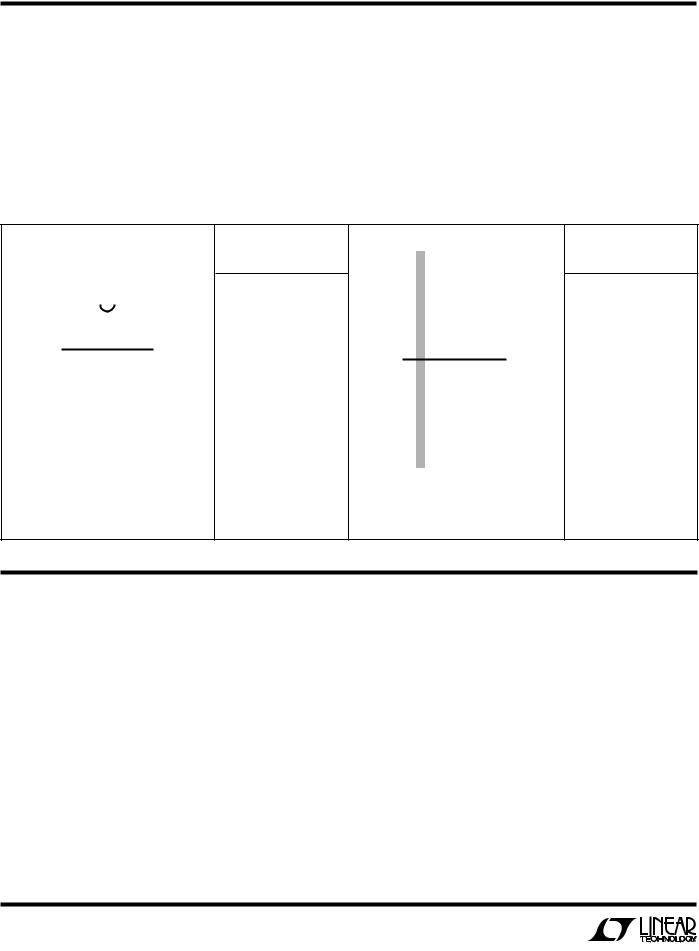
The LTC®1177-5/LTC1177-12 are isolated high side MOSFET drivers. When used with an external N-channel MOSFET, the LTC1177-5/LTC1177-12 form an isolated solid state switch for reliable bounce-free switching operation. The output does not require an auxiliary power supply to maintain an on-state condition.
Two lead frame capacitors are used to transfer energy from the input to drive the gate of the MOSFET and provide the necessary isolation. Unlike optoisolated FET drivers, the input current for the LTC1177-5 is only 1mA and 2.5mA for LTC1177-12. It also does not have the aging problems endemic to optocouplers.
Both devices provide 2500VRMS (1 minute) or 3000VRMS (1 second) of output-to-input isolation.
The LTC1177-5/LTC1177-12 are available in the 18-pin PDIP or 28-pin SW package.
 , LTC and LT are registered trademarks of Linear Technology Corporation.
TYPICAL APPLICATIOU
Isolated High Side Switch Input vs Output
|
f = 50Hz |
1 |
|
18 |
5V OR 12V |
VIN |
|||
|
0V |
|
GND1 |
|
|
|
|
|
|
|
|
|
|
LTC1177-5 |
|
V+ = 40V |
|
|
LTC1177-12 |
|
|
ISOLATION BARRIER |
||
|
|
|
||
+ |
|
7 |
NC |
12 |
47μF |
|
NC |
||
|
|
|
|
|
|
50V |
8 |
NC |
11 |
|
|
|
GND2 |
|
|
MTD3055EL |
9 |
OUT |
10 |
|
|
SENSE |
||
|
|
|
|
VOUT |
|
ROUT |
|
|
|
|
50Ω |
|
|
|
|
|
|
|
1177 TA01 |
VOUT
VIN
1177 TA02
1
LTC1177-5/LTC1177-12
ABSOLUTE
WAXIWUW
RATIUGS
Input Voltages |
|
Operating Temperature Range |
0°C to 70°C |
|
|
VIN (LTC1177-5) ....................... |
6V to (GND1 – 0.3V) |
Commercial ............................................. |
|
|
VIN (LTC1177-12) ................ |
13.2V to (GND1 – 0.3V) |
Industrial ........................................... |
– 40°C to 85°C |
|
Sense (LTC1177-5) ................... |
6V to (GND2 – 0.3V) |
Storage Temperature Range .................. |
–65°C to 150°C |
|
Sense (LTC1177-12) .............. |
12V to (GND2 – 0.3V) |
Lead Temperature (Soldering, 10 sec).................. |
300°C |
Output Voltages .......................... |
12V to (GND2 – 0.3V) |
|
|
|
|
|
|
|
|
|
|
|
|
|
PACKAGE/ORDER IUFORWATIOU
|
|
TOP VIEW |
|
|
VIN |
|
|
|
|
1 |
|
18 |
GND1 |
|
|
|
ISOLATION |
|
|
|
|
BARRIER |
|
|
NC |
|
|
|
NC |
7 |
|
12 |
||
NC |
|
|
|
GND2 |
8 |
|
11 |
||
OUT |
|
|
|
SENSE |
9 |
|
10 |
||
|
|
|
|
|
N PACKAGE
18-LEAD PDIP ISOLATION BARRIER
TJMAX = 125°C, θJA = 110°C/ W
ORDER PART
NUMBER
LTC1177CN-5 LTC1177CN-12 LTC1177IN-5 LTC1177IN-12
|
|
|
TOP VIEW |
|
|
NC |
|
|
|
|
|
1 |
|
|
28 |
NC |
|
VIN |
|
|
|
|
GND1 |
2 |
|
|
27 |
||
NC |
|
|
|
|
NC |
3 |
|
|
26 |
||
NC |
|
|
|
|
NC |
4 |
|
|
25 |
||
|
|
|
ISOLATION |
|
|
|
|
|
BARRIER |
|
|
|
|
|
|
|
|
NC |
11 |
|
|
18 |
NC |
NC |
|
|
|
|
GND2 |
12 |
|
|
17 |
||
OUT |
|
|
|
|
SENSE |
13 |
|
|
16 |
||
NC |
|
|
|
|
NC |
14 |
|
|
15 |
||
|
|
|
|
|
|
SW PACKAGE
28-LEAD PLASTIC SO WIDE ISOLATION BARRIER
TJMAX = 125°C, θJA = 125°C/ W
ORDER PART
NUMBER
LTC1177CSW-5 LTC1177CSW-12 LTC1177ISW-5 LTC1177ISW-12
Consult factory for Military grade parts.
ELECTRICAL CHARACTERISTICS VIN = 5V, TA = 25°C, unless otherwise noted.
|
|
|
|
|
LTC1177-5 |
|
|
SYMBOL |
PARAMETER |
CONDITIONS |
|
MIN |
TYP |
MAX |
UNITS |
|
|
|
|
|
|
|
|
VOUT |
Output Voltage (Refer to GND2) |
COUT = 1000pF, No Load (N Pkg) |
● |
6.5 |
7.5 |
10 |
V |
|
|
COUT = 1000pF, No Load, VIN = 4.75V (N Pkg) |
● |
5.5 |
6.5 |
10 |
V |
|
|
COUT = 1000pF, No Load (SW Pkg) |
● |
7.0 |
8.0 |
10 |
V |
|
|
COUT = 1000pF, No Load, VIN = 4.75V (SW Pkg) |
● |
6.0 |
7.0 |
10 |
V |
IIN |
Input Current |
CIN = 1000pF |
● |
|
1.0 |
1.5 |
mA |
ILIM |
Current Limit |
RSENSE = 1Ω (LTC1177C-5) |
● |
400 |
620 |
800 |
mA |
|
|
RSENSE = 1Ω (LTC1177I-5) |
● |
350 |
620 |
900 |
mA |
tON |
Turn-On Time |
COUT = 1000pF, No Load (LTC1177C-5) |
● |
|
1.0 |
4.0 |
ms |
|
|
COUT = 1000pF, No Load (LTC1177I-5) |
● |
|
1.0 |
4.5 |
ms |
tOFF |
Turn-Off Time |
COUT = 1000pF, No Load |
● |
|
1.0 |
1.8 |
ms |
VISO |
Isolation Voltage |
1 Minute (Note 1) |
|
2500 |
|
|
VRMS |
|
|
1 Second |
|
3000 |
|
|
VRMS |
tCM |
Common Mode Slew Rate |
VOUT < 1.5, COUT= 1000pF |
|
|
|
1000 |
V/μs |
2
LTC1177-5/LTC1177-12
ELECTRICAL CHARACTERISTICS VIN = 12V, TA = 25°C unless otherwise noted.
|
|
|
|
|
LTC1177-12 |
|
|
SYMBOL |
PARAMETER |
CONDITIONS |
|
MIN |
TYP |
MAX |
UNITS |
|
|
|
|
|
|
|
|
VOUT |
Output Voltage (Refer to GND2) |
COUT = 1000pF, No Load (LTC1177C-12, N Pkg) |
● |
4.65 |
5.2 |
8 |
V |
|
|
COUT = 1000pF, No Load (LTC1177C-12, SW Pkg) |
● |
5.00 |
5.7 |
8 |
V |
|
|
COUT = 1000pF, VIN = 11.4V (LTC1177C-12, N Pkg) |
● |
4.40 |
4.9 |
7 |
V |
|
|
COUT = 1000pF, VIN = 11.4V (LTC1177C-12, SW Pkg) |
● |
4.60 |
5.3 |
7 |
V |
|
|
COUT = 1000pF, No Load (LTC1177I-12, N Pkg) |
● |
4.50 |
5.2 |
8 |
V |
|
|
COUT = 1000pF, No Load (LTC1177I-12, SW Pkg) |
● |
4.75 |
5.7 |
8 |
V |
|
|
COUT = 1000pF, VIN = 11.4V (LTC1177I-12, SW Pkg) |
● |
4.50 |
5.3 |
7 |
V |
IIN |
Input Current |
CIN = 1000pF (LTC1177C-12) |
● |
|
2.5 |
3.0 |
mA |
|
|
CIN = 1000pF (LTC1177I-12) |
● |
|
2.5 |
3.4 |
mA |
ILIM |
Current Limit |
RSENSE = 1Ω (LTC1177C-12) |
● |
400 |
620 |
800 |
mA |
|
|
RSENSE = 1Ω (LTC1177I-12) |
● |
350 |
620 |
900 |
mA |
tON |
Turn-On Time |
COUT = 1000pF, No Load (LTC1177C-12) |
● |
|
1.0 |
2.5 |
ms |
|
|
COUT = 1000pF, No Load (LTC1177I-12, N Pkg) |
|
|
1.0 |
|
ms |
|
|
COUT = 1000pF, No Load (LTC1177I-12, SW Pkg) |
● |
|
1.0 |
2.5 |
ms |
tOFF |
Turn-Off Time |
COUT = 1000pF, No Load (LTC1177C-12) |
● |
|
1.0 |
1.2 |
ms |
|
|
COUT = 1000pF, No Load (LTC1177I-12, N Pkg) |
|
|
1.0 |
|
ms |
|
|
COUT = 1000pF, No Load (LTC1177I-12, SW Pkg) |
● |
|
1.0 |
1.5 |
ms |
VISO |
Isolation Voltage |
1 Minute (Note 1) |
|
2500 |
|
|
VRMS |
|
|
1 Second |
|
3000 |
|
|
VRMS |
TCM |
Common Mode Slew Rate |
VOUT < 1.5V, COUT= 1000pF |
|
|
|
1000 |
V/μs |
The ● denotes specifications which apply over the full operating temperature range.
Note 1: Value derived from 1 second test.
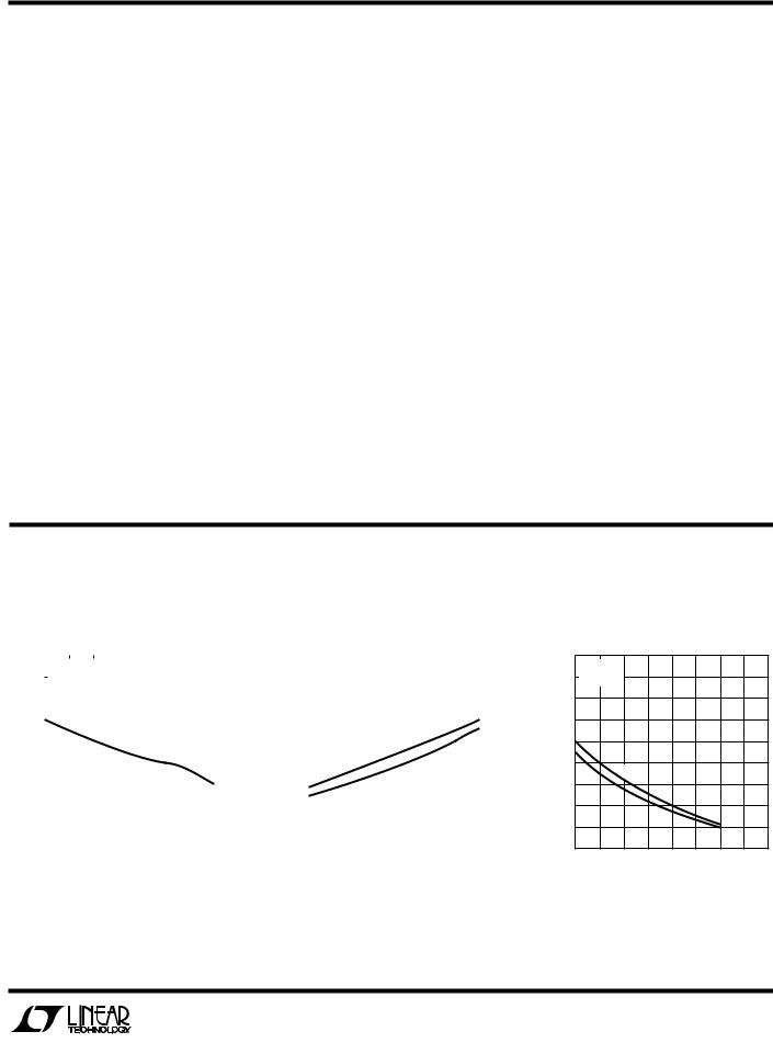
TYPICAL PERFORWAUCE CHARACTERISTICS
LTC1177-5 |
LTC1177-5 |
Turn-Off Time to VOUT = 1V |
Turn-On Time to VOUT = 4.5V |
vs Temperature |
vs Temperature |
|
1.8 |
|
|
|
|
|
|
|
|
|
|
|
|
|
1.8 |
|
|
|
|
|
|
|
|
|
|
|
|
|
|
VIN = 5V |
|
|
|
|
|
|
|
|
|
|
|
VIN = 5V |
|
|
|
|
|
|
|||||
|
1.6 |
|
COUT = 1000pF |
|
|
|
|
|
|
|
|
|
1.6 |
|
COUT = 1000pF |
|
|
|
|
|
|
|||||
|
|
|
|
|
|
|
|
|
|
|
|
|
|
|
|
|||||||||||
(ms) |
1.4 |
|
|
|
|
|
|
|
|
|
|
|
|
(ms) |
1.4 |
|
|
|
|
|
|
|
|
|
|
|
|
|
|
|
|
|
|
|
|
|
|
|
|
|
|
|
|
|
|
|
|
|
|
||||
1.2 |
|
|
|
|
|
|
|
|
|
|
|
|
1.2 |
|
|
|
|
|
|
|
|
|
|
|
||
|
|
|
|
|
|
|
|
|
|
|
|
|
|
|
|
|
|
|
|
|
|
|
||||
TIME |
1.0 |
|
|
|
|
|
|
|
|
|
|
|
|
TIME |
1.0 |
|
|
|
|
|
|
|
|
|
|
|
OFF-TURN |
|
|
|
|
|
|
|
|
|
|
|
|
ON-TURN |
|
|
|
N18 |
|
|
|
|
|
|
|
||
0.8 |
|
|
|
|
|
|
|
|
|
|
|
|
0.8 |
|
|
|
|
|
|
|
|
|
|
|||
|
|
|
|
|
|
|
|
|
|
|
|
|
|
|
|
|
|
|
|
|
|
|
||||
|
0.6 |
|
|
|
|
|
|
N18, SW28 |
|
|
|
|
0.6 |
|
|
|
|
|
SW28 |
|
|
|
|
|||
|
|
|
|
|
|
|
|
|
|
|
|
|
|
|
|
|
|
|
|
|
|
|
|
|
||
|
0.4 |
|
|
|
|
|
|
|
|
|
|
|
|
|
0.4 |
|
|
|
|
|
|
|
|
|
|
|
|
|
|
|
|
|
|
|
|
|
|
|
|
|
|
|
|
|
|
|
|
|
|
|
|
||
|
0.2 |
|
|
|
|
|
|
|
|
|
|
|
|
|
0.2 |
|
|
|
|
|
|
|
|
|
|
|
|
|
|
|
|
|
|
|
|
|
|
|
|
|
|
|
|
|
|
|
|
|
|
|
|
||
|
0 |
|
|
|
|
|
|
|
|
|
|
|
|
|
0 |
|
|
|
|
|
|
|
|
|
|
|
|
|
|
|
|
|
|
|
|
|
|
|
|
|
|
|
|
|
|
|
|
|
|
|
|
||
|
–55 –25 0 25 50 75 100 125 150 |
|
–55 –25 0 25 50 75 100 125 150 |
|||||||||||||||||||||||
|
|
|
|
|
TEMPERATURE (°C) |
|
|
|
|
|
TEMPERATURE (°C) |
|||||||||||||||
|
|
|
|
|
|
|
|
|
|
|
1177-5 G01 |
|
|
|
|
|
|
|
|
|
|
1177-5 G02 |
||||
OUTPUT CURRENT (μA)
LTC1177-5
Output Current vs Output Voltage
18
TA = 25°C 16 VIN = 5V
14
12
10
8
SW28
6
N18
4
2
0
0 |
1 |
2 |
3 |
4 |
5 |
6 |
7 |
8 |
OUTPUT VOLTAGE (V)
1177-5 G03
3
 Loading...