


Linear Technology LT1636IN8, LT1636IDD, LT1636CN8, LT1636CMS8, LT1636CDD Datasheet
...
FEATURES
■Rail-to-Rail Input and Output
■Micropower: 50µA IQ, 44V Supply
■Tiny 3mm × 3mm × 0.8mm DFN Package
■Operating Temperature Range: – 40°C to 125°C
■Over-The-Top®: Input Common Mode Range Extends 44V Above VEE, Independent of VCC
■Low Input Offset Voltage: 225µV Max
■Specified on 3V, 5V and ±15V Supplies
■High Output Current: 18mA
■Output Shutdown
■Output Drives 10,000pF with Output Compensation
■Reverse Battery Protection to 27V
■High Voltage Gain: 2000V/mV
■High CMRR: 110dB
■220kHz Gain-Bandwidth Product
APPLICATIOUS
■Batteryor Solar-Powered Systems Portable Instrumentation Sensor Conditioning
■Supply Current Sensing
■Battery Monitoring
■MUX Amplifiers
■4mA to 20mA Transmitters
LT1636
Over-The-Top
Micropower Rail-to-Rail
Input and Output Op Amp
DESCRIPTIOU
The LT®1636 op amp operates on all single and split supplies with a total voltage of 2.7V to 44V drawing less than 50µA of quiescent current. The LT1636 can be shut down, making the output high impedance and reducing the quiescent current to 4µA. The LT1636 has a unique input stage that operates and remainshighimpedancewhenabovethepositivesupply.The inputs take 44V both differential and common mode, even when operating on a 3V supply. The output swings to both supplies. Unlike most micropower op amps, the LT1636 can drive heavy loads; its rail-to-rail output drives 18mA. The LT1636 is unity-gain stable into all capacitive loads up to 10,000pF when a 0.22µF and 150Ω compensation network is used.
The LT1636 is reverse supply protected: it draws no current for reverse supply up to 27V. Built-in resistors protect the inputs for faults below the negative supply up to 22V. There is no phase reversal of the output for inputs 5V below VEE or 44V above VEE, independent of VCC.
The LT1636 op amp is available in the 8-pin MSOP, PDIP and SO packages. For space limited applications the LT1636 is available in a 3mm × 3mm × 0.8mm dual fine pitch leadless package (DFN).
, LTC and LT are registered trademarks of Linear Technology Corporation.
Over-The-Top is a registered trademark of Linear Technology Corporation.
TYPICAL APPLICATIOU
Input Bias Current vs Common Mode Voltage
Over-The-Top Current Source with Shutdown |
|
5000 |
|
|
|
|
|
|
|
|
||||
|
VS = 5V, 0V |
|
|
|
|
|
|
|||||||
|
|
|
4V TO |
|
3000 |
|
|
|
|
|
|
|
|
|
|
|
|
(nA) |
1000 |
|
|
|
|
|
|
|
|
||
|
LT1004-1.2 |
|
44V |
|
|
|
|
|
|
|
|
|
||
|
|
|
|
|
|
|
|
|
|
|
|
|
||
|
|
|
|
|
|
|
|
|
|
|
|
|
|
|
|
R* |
R |
|
|
CURRENT |
|
|
|
|
|
|
|
|
|
|
1M |
|
|
40 |
|
|
|
|
|
|
|
|
||
|
|
|
|
|
|
|
|
|
|
|
|
|||
|
|
|
|
|
|
|
|
|
|
|
|
|
|
|
|
+ |
|
|
|
BIAS |
30 |
|
|
|
|
|
|
|
|
|
LT1636 |
TPO610 |
|
20 |
TA = – 55°C |
|
|
|
|
|
|
|||
|
|
INPUT |
|
|
|
|
|
|
||||||
|
– |
|
IOUT = |
1.2 |
10 |
|
TA = 125°C |
|
|
|
|
|
||
|
|
IOUT |
|
R |
|
0 |
|
|
|
|
|
|
||
|
|
e.g., 10mA = 120Ω |
|
|
TA = 25°C |
|
|
|
|
|
|
|||
|
|
|
|
|
|
|
|
|
|
|
|
|
|
|
SHDN |
*OPTIONAL FOR LOW OUTPUT CURRENTS |
1636 TA01 |
|
–10 |
4.4 |
4.8 |
|
|
|
|
|
50 |
||
|
4.0 |
5.2 |
10 |
20 |
30 |
40 |
||||||||
|
|
|
|
|
|
|||||||||
|
|
|
|
|
|
|
COMMON MODE VOLTAGE (V) |
|
|
|||||
|
|
|
|
|
|
|
|
|
|
|
|
|
1636 G03 |
|
1636fb
1
LT1636
ABSOLUTE WMAXIWMUWM RATINGSU |
(Note 1) |
|
..............................Total Supply Voltage (V+ to V –) |
|
44V |
Input Differential Voltage ......................................... |
|
44V |
Input Current ...................................................... |
±25mA |
|
Shutdown Pin Voltage Above V – ............................. |
|
32V |
Shutdown Pin Current ....................................... |
±10mA |
|
Output Short-Circuit Duration (Note 2) ......... |
Continuous |
|
Operating Temperature Range (Note 3) |
– 40°C to 85°C |
|
LT1636C/LT1636I .............................. |
||
LT1636H .......................................... |
– 40°C to 125°C |
|
Specified Temperature Range (Note 4) |
– 40°C to 85°C |
LT1636C/LT1636I .............................. |
|
LT1636H .......................................... |
– 40°C to 125°C |
Junction Temperature........................................... |
150°C |
Junction Temperature (DD Package) ................... |
125°C |
Storage Temperature Range ................. |
– 65°C to 150°C |
Storage Temperature Range |
– 65°C to 125°C |
(DD Package) ....................................... |
|
Lead Temperature (Soldering, 10 sec).................. |
300°C |
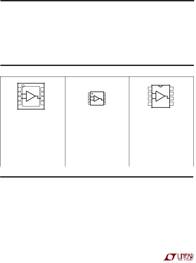
PACKAGE/ORDER IUFORWATIOU |
|
|
|
|
|
|
|||||
|
|
TOP VIEW |
|
|
|
|
|
|
TOP VIEW |
|
|
|
|
|
|
|
|
|
|
|
|
||
NULL |
1 |
8 |
NULL |
TOP VIEW |
|
|
NULL |
1 |
8 |
NULL |
|
–IN |
2 |
7 |
V+ |
NULL 1 |
8 |
NULL |
–IN |
2 |
7 |
V+ |
|
+IN |
3 |
6 |
OUT |
–IN 2 |
7 |
V+ |
+IN |
3 |
6 |
OUT |
|
+IN 3 |
6 |
OUT |
|||||||||
V– |
|
|
|
|
|
|
|
||||
4 |
5 |
SHDN |
V– 4 |
5 |
SHDN |
V– |
4 |
5 |
SHDN |
||
|
|
|
|
MS8 PACKAGE |
|
|
N8 PACKAGE |
S8 PACKAGE |
|||
|
|
DD PACKAGE |
|
8-LEAD PLASTIC MSOP |
|||||||
|
|
|
8-LEAD PDIP |
8-LEAD PLASTIC SO |
|||||||
8-LEAD (3mm × 3mm) PLASTIC DFN |
TJMAX = 150°C, θJA = 250°C/W |
||||||||||
TJMAX = 150°C, θJA = 150°C/W (N8) |
|||||||||||
TJMAX = 125°C, θJA = 160°C/W (NOTE 2) |
|
|
|
||||||||
|
|
|
TJMAX = 150°C, θJA = 190°C/W (S8) |
||||||||
UNDERSIDE METAL CONNECTED TO V– |
|
|
|
||||||||
|
|
|
|
|
|
|
|||||
ORDER PART |
DD PART* |
ORDER PART |
MS8 PART |
ORDER PART |
S8 PART |
NUMBER |
MARKING |
NUMBER |
MARKING |
NUMBER |
MARKING |
|
|
|
|
|
|
LT1636CDD |
LAAJ |
LT1636CMS8 |
LTCL |
LT1636CN8 |
1636 |
LT1636IDD |
|
|
|
LT1636CS8 |
1636I |
|
|
|
|
LT1636IN8 |
1636H |
|
|
|
|
LT1636IS8 |
|
|
|
|
|
LT1636HS8 |
|
*The temperature grades are identified by a label on the shipping container. Consult factory for parts specified with wider operating temperature ranges.
3V AUD 5V ELECTRICAL CHARACTERISTICS
The ● denotes the specifications which apply over the full operating temperature range of –40°C ≤ TA ≤ 85°C.
VS = 3V, 0V; VS = 5V, 0V; VCM = VOUT = half supply unless otherwise specified. (Note 4)
|
|
|
|
LT1636C/LT1636I |
|
|
||
SYMBOL |
PARAMETER |
CONDITIONS |
|
MIN |
TYP |
MAX |
UNITS |
|
VOS |
Input Offset Voltage |
N8 Package |
|
|
50 |
225 |
V |
|
|
|
0°C ≤ TA ≤ 70°C |
● |
|
|
400 |
V |
|
|
|
– 40°C ≤ TA ≤ 85°C |
● |
|
|
550 |
V |
|
|
|
S8 Package |
|
|
50 |
225 |
V |
|
|
|
0°C ≤ TA ≤ 70°C |
● |
|
|
600 |
V |
|
|
|
– 40°C ≤ TA ≤ 85°C |
● |
|
|
750 |
V |
|
|
|
MS8 Package |
|
|
50 |
225 |
V |
|
|
|
0°C ≤ TA ≤ 70°C |
● |
|
|
700 |
V |
|
|
|
– 40°C ≤ TA ≤ 85°C |
● |
|
|
850 |
V |
|
|
|
|
|
|
|
|
1636fb |
|
|
|
|
|
|
|
|
|
|
|
|
|
|
|
|
|
|
|
2

LT1636
3V AUD 5V ELECTRICAL CHARACTERISTICS
The ● denotes the specifications which apply over the full operating temperature range of –40°C ≤ TA ≤ 85°C.
VS = 3V, 0V; VS = 5V, 0V; VCM = VOUT = half supply unless otherwise specified. (Note 4)
|
|
|
|
|
LT1636C/LT1636I |
|
|
|
||
SYMBOL |
|
PARAMETER |
CONDITIONS |
|
MIN |
TYP |
MAX |
UNITS |
|
|
|
|
|
DD Package |
|
|
75 |
425 |
µV |
||
|
|
|
0°C ≤ TA ≤ 70°C |
● |
|
|
900 |
µV |
||
|
|
|
– 40°C ≤ TA ≤ 85°C |
● |
|
|
1050 |
µV |
||
|
|
Input Offset Voltage Drift (Note 9) |
N8 Package, – 40°C ≤ TA ≤ 85°C |
● |
|
1 |
5 |
µV/°C |
||
|
|
|
S8 Package, – 40°C ≤ TA ≤ 85°C |
● |
|
2 |
8 |
µV/°C |
||
|
|
|
MS8 Package, – 40°C ≤ TA ≤ 85°C |
● |
|
2 |
10 |
µV/°C |
||
|
|
|
DD Package, – 40°C ≤ TA ≤ 85°C |
● |
|
2 |
10 |
µV/°C |
||
IOS |
|
Input Offset Current |
|
● |
|
0.1 |
0.8 |
|
nA |
|
|
|
|
VCM = 44V (Note 5) |
● |
|
|
0.6 |
µA |
||
IB |
|
Input Bias Current |
|
● |
|
5 |
8 |
nA |
||
|
|
|
VCM = 44V (Note 5) |
● |
|
3 |
6 |
µA |
||
|
|
|
VS = 0V |
|
|
0.1 |
|
|
nA |
|
|
|
Input Noise Voltage |
0.1Hz to 10Hz |
|
|
0.7 |
|
µVP-P |
||
en |
|
Input Noise Voltage Density |
f = 1kHz |
|
|
52 |
|
nV/√ |
|
|
|
|
|
|
Hz |
||||||
in |
|
Input Noise Current Density |
f = 1kHz |
|
|
0.035 |
|
pA/√ |
|
|
|
|
|
|
Hz |
||||||
RIN |
|
Input Resistance |
Differential |
|
6 |
10 |
|
MΩ |
||
|
|
|
Common Mode, VCM = 0V to 44V |
|
7 |
15 |
|
MΩ |
||
CIN |
|
Input Capacitance |
|
|
|
4 |
|
|
pF |
|
|
|
Input Voltage Range |
|
● |
0 |
|
44 |
|
V |
|
CMRR |
|
Common Mode Rejection Ratio |
VCM = 0V to VCC – 1V |
● |
84 |
110 |
|
|
dB |
|
|
|
(Note 5) |
VCM = 0V to 44V (Note 8) |
● |
86 |
98 |
|
|
dB |
|
AVOL |
|
Large-Signal Voltage Gain |
VS = 3V, VO = 500mV to 2.5V, RL = 10k |
|
200 |
1300 |
|
V/mV |
||
|
|
|
VS = 3V, 0°C ≤ TA ≤ 70°C |
● |
133 |
|
|
V/mV |
||
|
|
|
VS = 3V, – 40°C ≤ TA ≤ 85°C |
● |
100 |
|
|
V/mV |
||
|
|
|
VS = 5V, VO = 500mV to 4.5V, RL = 10k |
|
400 |
2000 |
|
V/mV |
||
|
|
|
VS = 5V, 0°C ≤ TA ≤ 70°C |
● |
250 |
|
|
V/mV |
||
|
|
|
VS = 5V, – 40°C ≤ TA ≤ 85°C |
● |
200 |
|
|
V/mV |
||
VOL |
|
Output Voltage Swing LOW |
No Load |
● |
|
2 |
10 |
mV |
|
|
|
|
|
ISINK = 5mA |
● |
|
480 |
875 |
mV |
||
|
|
|
VS = 5V, ISINK = 10mA |
● |
|
860 |
1600 |
mV |
|
|
VOH |
|
Output Voltage Swing HIGH |
VS = 3V, No Load |
● |
2.95 |
2.985 |
|
|
V |
|
|
|
|
VS = 3V, ISOURCE = 5mA |
● |
2.55 |
2.8 |
|
|
V |
|
|
|
|
VS = 5V, No Load |
● |
4.95 |
4.985 |
|
|
V |
|
|
|
|
VS = 5V, ISOURCE = 10mA |
● |
4.30 |
4.75 |
|
|
V |
|
ISC |
|
Short-Circuit Current (Note 2) |
VS = 3V, Short to GND |
|
7 |
15 |
|
mA |
|
|
|
|
|
VS = 3V, Short to VCC |
|
20 |
42 |
|
mA |
|
|
|
|
|
VS = 5V, Short to GND |
|
12 |
25 |
|
mA |
||
|
|
|
VS = 5V, Short to VCC |
|
25 |
50 |
|
mA |
|
|
PSRR |
|
Power Supply Rejection Ratio |
VS = 2.7V to 12.5V, VCM = VO = 1V |
● |
90 |
103 |
|
|
dB |
|
|
|
Reverse Supply Voltage |
IS = – 100µA |
● |
27 |
40 |
|
|
V |
|
IS |
|
Supply Current |
(Note 6) |
|
|
42 |
55 |
µA |
||
|
|
|
|
● |
|
|
60 |
µA |
||
|
|
Supply Current, SHDN |
VPIN5 = 2V, No Load (Note 6) |
● |
|
4 |
12 |
µA |
||
ISD |
|
Shutdown Pin Current |
VPIN5 = 0.3V, No Load (Note 6) |
● |
|
0.5 |
15 |
|
nA |
|
|
|
|
VPIN5 = 2V, No Load (Note 5) |
● |
|
1.1 |
5 |
µA |
||
|
|
Output Leakage Current, SHDN |
VPIN5 = 2V, No Load (Note 6) |
● |
|
0.05 |
1 |
µA |
||
|
|
Maximum Shutdown Pin Current |
VPIN5 = 32V, No Load (Note 5) |
● |
|
27 |
150 |
µA |
||
tON |
|
Turn-On Time |
VPIN5 = 5V to 0V, RL = 10k |
|
|
120 |
|
|
µs |
|
tOFF |
|
Turn-Off Time |
VPIN5 = 0V to 5V, RL = 10k |
|
|
2.5 |
|
|
µs |
|
|
|
|
|
|
|
|
|
1636fb |
|
|
|
|
|
|
|
|
|
|
|
|
|
|
|
|
|
|
|
|
|
|
|
|
|
|
|
|
|
|
|
|
3 |
|
|
|
|
|
|
|
|
|
|
|||
|
|
|
|
|
|
|
|
|||

LT1636
3V AUD 5V ELECTRICAL CHARACTERISTICS
The ● denotes the specifications which apply over the full operating temperature range of –40°C ≤ TA ≤ 85°C.
VS = 3V, 0V; VS = 5V, 0V; VCM = VOUT = half supply unless otherwise specified. (Note 4)
|
|
|
|
LT1636C/LT1636I |
|
||
SYMBOL |
PARAMETER |
CONDITIONS |
|
MIN |
TYP |
MAX |
UNITS |
GBW |
Gain Bandwidth Product |
f = 1kHz |
|
110 |
200 |
|
kHz |
|
(Note 5) |
0°C ≤ TA ≤ 70°C |
● |
100 |
|
|
kHz |
|
|
– 40°C ≤ TA ≤ 85°C |
● |
90 |
|
|
kHz |
SR |
Slew Rate |
AV = – 1, RL = ∞ |
|
0.035 |
0.07 |
|
V/µs |
|
(Note 7) |
0°C ≤ TA ≤ 70°C |
● |
0.031 |
|
|
V/µs |
|
|
– 40°C ≤ TA ≤ 85°C |
● |
0.030 |
|
|
V/µs |
±15V ELECTRICAL CHARACTERISTICS
The ● denotes the specifications which apply over the full operating temperature range of –40°C ≤ TAÊ≤Ê 85°C. VS = ±15V, VCM = 0V, VOUT = 0V, VSHDN = V – unless otherwise specified. (Note 4)
|
|
|
|
LT1636C/LT1636I |
|
|
|
||
SYMBOL |
PARAMETER |
CONDITIONS |
|
MIN |
TYP |
MAX |
UNITS |
||
|
|
|
|
|
|
|
|
|
|
VOS |
Input Offset Voltage |
N8 Package |
|
|
100 |
450 |
µV |
||
|
|
0°C ≤ TA ≤ 70°C |
● |
|
|
550 |
µV |
||
|
|
– 40°C ≤ TA ≤ 85°C |
● |
|
|
700 |
µV |
|
|
|
|
S8 Package |
|
|
100 |
450 |
µV |
||
|
|
0°C ≤ TA ≤ 70°C |
● |
|
|
750 |
µV |
||
|
|
– 40°C ≤ TA ≤ 85°C |
● |
|
|
900 |
µV |
|
|
|
|
MS8 Package |
|
|
100 |
450 |
µV |
||
|
|
0°C ≤ TA ≤ 70°C |
● |
|
|
850 |
µV |
||
|
|
– 40°C ≤ TA ≤ 85°C |
● |
|
|
1000 |
µV |
|
|
|
|
DD Package |
|
|
125 |
650 |
µV |
||
|
|
0°C ≤ TA ≤ 70°C |
● |
|
|
1050 |
µV |
||
|
|
– 40°C ≤ TA ≤ 85°C |
● |
|
|
1200 |
µV |
|
|
|
Input Offset Voltage Drift (Note 9) |
N8 Package, – 40°C ≤ TA ≤ 85°C |
● |
|
1 |
4 |
µV/°C |
||
|
|
S8 Package, – 40°C ≤ TA ≤ 85°C |
● |
|
2 |
8 |
µV/°C |
||
|
|
MS8 Package, – 40°C ≤ TA ≤ 85°C |
● |
|
2 |
10 |
µV/°C |
||
|
|
DD Package, – 40°C ≤ TA ≤ 85°C |
● |
|
2 |
10 |
µV/°C |
|
|
IOS |
Input Offset Current |
|
● |
|
0.2 |
1.0 |
nA |
|
|
IB |
Input Bias Current |
|
● |
|
4 |
10 |
nA |
|
|
|
Input Noise Voltage |
0.1Hz to 10Hz |
|
|
1 |
|
µVP-P |
||
en |
Input Noise Voltage Density |
f = 1kHz |
|
|
52 |
|
nV/√ |
|
|
|
|
|
Hz |
||||||
in |
Input Noise Current Density |
f = 1kHz |
|
|
0.035 |
|
pA/√ |
|
|
|
|
|
Hz |
||||||
RIN |
Input Resistance |
Differential |
|
5.2 |
13 |
|
MΩ |
||
|
|
Common Mode, VCM = – 15V to 14V |
|
|
12000 |
|
MΩ |
|
|
CIN |
Input Capacitance |
|
|
|
4 |
|
|
pF |
|
|
Input Voltage Range |
|
● |
– 15 |
|
29 |
|
V |
|
|
|
|
|
|
|
|
|
|
|
CMRR |
Common Mode Rejection Ratio |
VCM = – 15V to 29V |
● |
86 |
103 |
|
dB |
|
|
AVOL |
Large-Signal Voltage Gain |
VO = ±14V, RL = 10k |
|
100 |
500 |
|
V/mV |
||
|
|
0°C ≤ TA ≤ 70°C |
● |
75 |
|
|
V/mV |
||
|
|
– 40°C ≤ TA ≤ 85°C |
● |
50 |
|
|
V/mV |
|
|
VOL |
Output Voltage Swing LOW |
No Load |
● |
|
– 14.997 |
– 14.95 |
|
V |
|
|
|
ISINK = 5mA |
● |
|
– 14.500 |
– 14.07 |
|
V |
|
|
|
ISINK = 10mA |
● |
|
– 14.125 |
– 13.35 |
|
V |
|
VOH |
Output Voltage Swing HIGH |
No Load |
● |
14.9 |
14.975 |
|
|
V |
|
|
|
ISOURCE = 5mA |
● |
14.5 |
14.750 |
|
|
V |
|
|
|
ISOURCE = 10mA |
● |
14.3 |
14.650 |
|
|
V |
|
|
|
|
|
|
|
|
1636fb |
||
|
|
|
|
|
|
|
|
|
|
|
|
|
|
|
|
|
|
|
|
4

LT1636
±15V ELECTRICAL CHARACTERISTICS
The ● denotes the specifications which apply over the full operating temperature range of –40°C ≤ TAÊ≤Ê 85°C, otherwise specifications are at TA = 25°C. VS = ±15V, VCM = 0V, VOUT = 0V, VSHDN = V – unless otherwise specified. (Note 4)
|
|
|
|
LT1636C/LT1636I |
|
||
SYMBOL |
PARAMETER |
CONDITIONS |
|
MIN |
TYP |
MAX |
UNITS |
|
|
|
|
|
|
|
|
ISC |
Short-Circuit Current (Note 2) |
Short to GND |
|
±18 |
±30 |
|
mA |
|
|
0°C ≤ TA ≤ 70°C |
● |
±15 |
|
|
mA |
|
|
– 40°C ≤ TA ≤ 85°C |
● |
±10 |
|
|
mA |
PSRR |
Power Supply Rejection Ratio |
VS = ±1.35V to ±22V |
● |
90 |
114 |
|
dB |
IS |
Supply Current |
|
|
|
50 |
70 |
A |
|
|
|
● |
|
|
85 |
A |
|
Positive Supply Current, SHDN |
VPIN5 = – 20V, VS = ±22V, No Load |
● |
|
12 |
30 |
A |
ISHDN |
Shutdown Pin Current |
VPIN5 = – 21.7V, VS = ±22V, No Load |
● |
|
0.7 |
15 |
nA |
|
|
VPIN5 = – 20V, VS = ±22V, No Load |
● |
|
1.2 |
8 |
A |
|
Maximum Shutdown Pin Current |
VPIN5 = 32V, VS = ±22V |
● |
|
27 |
150 |
A |
|
Output Leakage Current, SHDN |
VPIN5 = – 20V, VS = ±22V, No Load |
● |
|
0.1 |
2 |
A |
GBW |
Gain Bandwidth Product |
f = 1kHz |
|
125 |
220 |
|
kHz |
|
|
0°C ≤ TA ≤ 70°C |
● |
110 |
|
|
kHz |
|
|
– 40°C ≤ TA ≤ 85°C |
● |
100 |
|
|
kHz |
SR |
Slew Rate |
AV = – 1, RL = ∞, VO = ±10V Measured at ±5V |
|
0.0375 |
0.075 |
|
V/ s |
|
|
0°C ≤ TA ≤ 70°C |
● |
0.033 |
|
|
V/ s |
|
|
– 40°C ≤ TA ≤ 85°C |
● |
0.030 |
|
|
V/ s |
3V AUD 5V ELECTRICAL CHARACTERISTICS
The ● denotes the specifications which apply over the full operating temperature range of –40°C ≤ TA ≤ 125°C.
VS = 3V, 0V; VS = 5V, 0V; VCM = VOUT = half supply unless otherwise specified. (Note 4)
|
|
|
|
|
LT1636H |
|
|
SYMBOL |
PARAMETER |
CONDITIONS |
|
MIN |
TYP |
MAX |
UNITS |
|
|
|
|
|
|
|
|
VOS |
Input Offset Voltage |
|
|
|
50 |
325 |
V |
|
|
|
● |
|
|
3 |
mV |
|
|
|
|
|
|
|
|
|
Input Offset Voltage Drift (Note 9) |
|
● |
|
3 |
10 |
V/°C |
|
|
|
|
|
|
|
|
IOS |
Input Offset Current |
|
● |
|
|
3 |
nA |
|
|
VCM = 44V (Note 5) |
● |
|
|
1 |
A |
IB |
Input Bias Current |
|
● |
|
|
30 |
nA |
|
|
VCM = 44V (Note 5) |
● |
|
|
10 |
A |
|
Input Voltage Range |
|
● |
0.3 |
|
44 |
V |
CMRR |
Common Mode Rejection Ratio |
VCM = 0.3V to VCC – 1V |
● |
72 |
|
|
dB |
|
(Note 5) |
VCM = 0.3V to 44V |
● |
74 |
|
|
dB |
AVOL |
Large-Signal Voltage Gain |
VS = 3V, VO = 500mV to 2.5V, RL = 10k |
|
200 |
1300 |
|
V/mV |
|
|
|
● |
20 |
|
|
V/mV |
|
|
VS = 5V, VO = 500mV to 4.5V, RL = 10k |
|
400 |
2000 |
|
V/mV |
|
|
|
● |
35 |
|
|
V/mV |
VOL |
Output Voltage Swing LOW |
No Load |
● |
|
|
15 |
mV |
|
|
ISINK = 2.5mA |
● |
|
|
875 |
mV |
VOH |
Output Voltage Swing HIGH |
VS = 3V, No Load |
● |
2.925 |
|
|
V |
|
|
VS = 3V, ISOURCE = 5mA |
● |
2.35 |
|
|
V |
|
|
VS = 5V, No Load |
● |
4.925 |
|
|
V |
|
|
VS = 5V, ISOURCE = 10mA |
● |
4.10 |
|
|
V |
PSRR |
Power Supply Rejection Ratio |
VS = 2.7V to 12.5V, VCM = VO = 1V |
● |
80 |
|
|
dB |
|
Minimum Supply Voltage |
|
● |
2.7 |
|
|
V |
|
|
|
|
|
|
|
1636fb |
|
|
|
|
|
|
|
|
|
|
|
|
|
|
|
|
|
|
|
|
|
|
|
5 |
|
|
|
|
|
|
|
|
|
|
|
|
|
|
|
 Loading...