


Linear Technology LT1181AIN, LT1181ACSW, LT1181ACN, LT1180AMJ, LT1180AISW Datasheet
...FEATURES
■ESD Protection over ±10kV
■Uses Small Capacitors: 0.1 F
■120kBaud Operation for RL = 3k, CL = 2500pF
■250kBaud Operation for RL = 3k, CL = 1000pF
■Outputs Withstand ±30V Without Damage
■CMOS Comparable Low Power: 40mW
■Operates from a Single 5V Supply
■Rugged Bipolar Design
■Outputs Assume a High Impedance State When Off or Powered Down
■Meets All RS232 Specifications
■Available With or Without Shutdown
■Absolutely No Latch-up
■Available in SO Package
APPLICATIOUS
■Portable Computers
■Battery-Powered Systems
■Power Supply Generator
■Terminals
■Modems
LT1180A/LT1181A
Low Power 5V RS232 Dual Driver/Receiver with 0.1 F Capacitors
DESCRIPTIOU
The LT®1180A/LT1181A are dual RS232 driver/receiver pairs with integral charge pump to generate RS232 voltage levels from a single 5V supply. These circuits feature rugged bipolar design to provide operating fault tolerance and ESD protection unmatched by competing CMOS designs. Using only 0.1 F external capacitors, these circuits consume only 40mW of power, and can operate to 120k baud even while driving heavy capacitive loads. New ESD structures on the chip allow the LT1180A/LT1181A to survive multiple ±10kV strikes, eliminating the need for costly TransZorbs® on the RS232 line pins. The LT1180A/ LT1181A are fully compliant with EIA RS232 standards. Driver outputs are protected from overload, and can be shorted to ground or up to ±30V without damage. During shutdown or power-off conditions, driver and receiver outputs are in a high impedance state, allowing line sharing.
The LT1181A is available in 16-pin DIP and SO packages. The LT1180A is supplied in 18-pin DIP and SO packages for applications which require shutdown.
 , LTC and LT are registered trademarks of Linear Technology Corporation.
TransZorb is a registered trademark of General Instruments, GSI
TYPICAL APPLICATIOU
|
+ |
2 |
|
17 |
5V INPUT |
Output Waveforms |
|
0.1 F |
|
|
|
||||
|
4 |
|
3 |
|
+ OUT |
|
|
|
|
|
V |
|
|||
|
|
|
|
+ |
|
||
|
|
|
|
|
|
|
|
|
|
LT1180A |
|
0.1 F |
|
DRIVER |
|
|
|
|
|
|
|
||
|
|
5 |
|
7 |
|
– OUT |
OUTPUT |
|
+ |
|
V |
RL = 3k |
|||
|
|
|
|
||||
|
|
|
|
0.1 |
|
|
CL = 2500pF |
0.1 F |
|
6 |
|
F |
|
|
|
|
|
+ |
|
|
|
||
|
|
|
|
|
|
||
|
|
12 |
|
|
|
|
|
|
|
|
15 |
RS232 OUTPUT |
RECEIVER |
||
LOGIC |
|
|
|
|
|||
|
|
|
|
|
|
ROUTPUT |
|
INPUTS |
|
|
|
|
|
|
|
|
11 |
|
8 |
RS232 OUTPUT |
CL = 50pF |
||
|
|
|
|
|
|
||
|
|
13 |
|
14 |
RS232 INPUT |
|
|
|
|
|
|
|
INPUT |
||
LOGIC |
|
|
5k |
|
|
|
|
|
|
|
|
|
|
||
OUTPUTS |
|
|
|
|
|
|
|
|
|
10 |
|
9 |
RS232 INPUT |
|
|
|
|
|
|
|
|
||
ON/OFF |
|
18 |
5k |
16 |
|
|
|
|
|
|
|
|
|
|
|
|
|
|
|
|
|
LT1180A • TA01 |
|
LT1180A • TA02
11801afb
1
LT1180A/LT1181A
ABSOLUTE
WAXIWUW
RATI GS |
(Note 1) |
U |
Supply Voltage (VCC) |
................................................ 6V |
V+ ........................................................................ |
13.2V |
V– ...................................................................... |
– 13.2V |
Input Voltage |
V – to V + |
Driver ........................................................... |
|
Receiver ............................................... |
– 30V to 30V |
ON/OFF ................................................. |
– 0.3V to 12V |
Output Voltage |
V + – 30V to V – + 30V |
Driver ...................................... |
|
Receiver .................................... |
– 0.3V to V CC + 0.3V |
Short-Circuit Duration |
|
V+ ................................................................... |
30 sec |
V– ................................................................... |
30 sec |
Driver Output .............................................. |
Indefinite |
Receiver Output .......................................... |
Indefinite |
Operating Temperature Range |
– 40°C to 85°C |
LT1180AI/LT1181AI .......................... |
|
LT1180AC/LT1181AC ............................. |
0°C to 70°C |
Storage Temperature Range ................ |
– 65°C to 150°C |
Lead Temperature (Soldering, 10 sec)................. |
300°C |
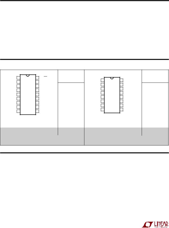
PACKAGE/ORDER IUFORWATIOU
|
TOP VIEW |
|
ORDER PART |
|
|
|
TOP VIEW |
|
ORDER PART |
||
|
|
|
|
C1+ |
1 |
VCC |
|||||
NC |
1 |
18 |
ON/OFF |
NUMBER |
16 |
NUMBER |
|||||
|
|
|
|
|
|
|
|||||
C1+ |
2 |
17 |
VCC |
|
V+ |
2 |
15 |
GND |
|
||
V+ |
3 |
16 |
GND |
|
|
||||||
LT1180ACN |
C1 |
– |
3 |
14 |
TR1 OUT |
LT1181ACN |
|||||
C1– |
4 |
15 |
TR1 OUT |
||||||||
C2+ |
5 |
14 |
REC1 IN |
LT1180ACSW |
C2+ |
4 |
13 |
REC1 IN |
LT1181ACSW |
||
C2– |
6 |
13 |
REC1 OUT |
LT1180AIN |
C2 |
– |
5 |
12 |
REC1 OUT |
LT1181AIN |
|
V– |
7 |
12 |
TR1 IN |
LT1180AISW |
V |
– |
6 |
11 |
TR1 IN |
LT1181AISW |
|
|
|
|
|
|
|
||||||
TR2 OUT |
8 |
11 |
TR2 IN |
|
TR2 OUT |
7 |
10 |
TR2 IN |
|
||
|
REC2 IN |
8 |
9 |
REC2 OUT |
|
||||||
REC2 IN |
9 |
10 |
REC2 OUT |
|
|
||||||
|
|
|
|
|
|
|
|||||
N PACKAGE |
SW PACKAGE |
|
N PACKAGE |
SW PACKAGE |
|
||||||
|
16-LEAD PDIP 16-LEAD PLASTIC SO (WIDE) |
|
|||||||||
18-LEAD PDIP 18-LEAD PLASTIC SO (WIDE) |
|
|
|||||||||
|
TJMAX = 125°C, θJA = 90°C/ W, θJC = 46°C/W (N) |
|
|||||||||
TJMAX = 125°C, θJA |
= 80°C/ W, θJC = 36°C/W (N) |
|
|
||||||||
|
TJMAX = 125°C, θJA = 95°C/ W, θJC = 27°C/W (SW) |
|
|||||||||
TJMAX = 125°C, θJA = 90°C/ W, θJC = 26°C/W (SW) |
|
|
|||||||||
|
|
|
|
|
|
|
|||||
J PACKAGE |
LT1180AMJ |
J PACKAGE |
LT1181AMJ |
18-LEAD CERDIP |
16-LEAD CERDIP |
||
TJMAX = 150°C, θJA = 100°C/W, θJC = 40°C/W (J) |
|
TJMAX = 150°C, θJA = 100°C/W, θJC = 40°C/W (J) |
|
OBSOLETE PACKAGE |
OBSOLETE PACKAGE |
Consider N Package for Alternate Source |
Consider N Package for Alternate Source |
Consult LTC Marketing for parts specified with wider operating temperature ranges.
ELECTRICAL CHARACTERISTICS The ● denotes specifications which apply over the operating temperature range (0°C ≤ TA ≤ 70°C for commercial grade, and –40°C ≤ TA ≤ 85°C for industrial grade. (Note 2)
PARAMETER |
CONDITIONS |
|
MIN |
TYP |
MAX |
UNITS |
||
|
|
|
|
|
|
|
|
|
Power Supply Generator |
|
|
|
|
|
|
||
V + Output |
|
|
|
7.9 |
|
V |
||
V – Output |
|
|
|
– 7.0 |
|
V |
||
Supply Current (VCC) |
(Note 3), TA = 25°C |
|
|
9 |
13 |
mA |
||
|
|
|
|
● |
|
|
16 |
mA |
Supply Current When OFF (VCC) |
Shutdown (Note 4) LT1180A Only |
● |
|
1 |
10 |
A |
||
Supply Rise Time |
C1 = C2 = C3 = C4 = 0.1 F |
|
|
0.2 |
|
ms |
||
Shutdown to Turn-On |
LT1180A Only |
|
|
0.2 |
|
ms |
||
|
|
Pin Thresholds |
Input Low Level (Device Shutdown) |
|
0.8 |
1.2 |
|
V |
ON/OFF |
● |
|
||||||
|
|
|
Input High Level (Device Enabled) |
● |
|
1.6 |
2.4 |
V |
|
|
|
|
|
|
|
|
11801afb |
|
|
|
|
|
|
|
|
|
|
|
|
|
|
|
|
|
|
2

LT1180A/LT1181A
ELECTRICAL CHARACTERISTICS The ● denotes specifications which apply over the operating temperature range (0°C ≤ TA ≤ 70°C for commercial grade, and – 40°C ≤ TA ≤ 85°C for industrial grade. (Note 2)
PARAMETER |
CONDITIONS |
|
|
MIN |
TYP |
MAX |
|
UNITS |
||||||
|
|
|
|
|
|
|
|
|
|
|
|
|
|
|
ON/OFF |
Pin Current |
0V ≤ VON/OFF |
≤ 5V |
|
● |
– 15 |
|
80 |
|
µA |
||||
Oscillator Frequency |
|
|
|
|
|
|
130 |
|
|
kHz |
||||
Driver |
|
|
|
|
|
|
|
|
|
|
|
|
||
|
|
|
|
|
|
|
|
|
|
|
|
|
|
|
Output Voltage Swing |
Load = 3k to GND |
Positive |
|
5.0 |
7.5 |
|
|
V |
||||||
|
|
|
|
|
|
|
|
Negative |
● |
|
– 6.3 |
– 5.0 |
|
V |
|
|
|
|
|
|
|
|
|
||||||
Logic Input Voltage Level |
Input Low Level (VOUT = High) |
|
● |
|
1.4 |
0.8 |
|
V |
||||||
Input High Level (VOUT = Low) |
|
|
|
|
● |
2.0 |
1.4 |
|
|
V |
||||
Logic Input Current |
0.8V ≤ VIN ≤ 2.0V |
|
● |
|
5 |
20 |
|
µA |
||||||
Output Short-Circuit Current |
VOUT = 0V |
|
|
±9 |
17 |
|
|
mA |
||||||
Output Leakage Current |
Shutdown VOUT = ±30V (Note 4) |
|
● |
|
10 |
100 |
|
µA |
||||||
Date Rate (Note 7) |
RL = 3k, CL = 2500pF |
|
|
120 |
|
|
|
kBaud |
||||||
|
|
|
|
|
RL = 3k, CL = 1000pF |
|
|
250 |
|
|
|
kBaud |
||
Slew Rate |
RL = 3k, CL = 51pF |
|
|
|
15 |
30 |
|
V/µs |
||||||
RL = 3k, CL = 2500pF |
|
|
|
|
|
4 |
7 |
|
|
V/µs |
||||
Propagation Delay |
Output Transition tHL High-to-Low (Note 5) |
|
|
0.6 |
1.3 |
|
µs |
|||||||
|
|
|
|
|
Output Transition tLH Low-to-High |
|
|
|
0.5 |
1.3 |
|
µs |
||
Receiver |
|
|
|
|
|
|
|
|
|
|
|
|||
|
|
|
|
|
|
|
|
|
|
|
|
|
|
|
Input Voltage Thresholds |
Input Low Threshold (VOUT = High) |
C Grade |
● |
0.8 |
1.3 |
|
|
V |
||||||
|
|
|
|
|
Input High Threshold (VOUT = Low) |
C Grade |
● |
|
1.7 |
2.4 |
|
V |
||
|
|
|
|
|
Input LowI, |
M Grade |
● |
0.2 |
1.3 |
|
|
V |
||
|
|
|
|
|
Input HighI, |
M Grade |
● |
|
1.7 |
3.0 |
|
V |
||
|
|
|
|
|
|
|
|
|
|
|
||||
Hysteresis |
|
|
|
|
● |
0.1 |
0.4 |
1.0 |
|
V |
||||
|
|
|
|
|
|
|
|
|
||||||
Input Resistance |
VIN = ±10V |
|
|
3 |
5 |
7 |
|
kΩ |
||||||
Output Leakage Current |
Shutdown (Note 4) 0 ≤ VOUT ≤ VCC |
|
● |
|
1 |
10 |
|
µA |
||||||
Output Voltage |
Output Low, IOUT = – 1.6mA |
|
● |
|
0.2 |
0.4 |
|
V |
||||||
|
|
|
|
|
Output High, IOUT = 160µA (VCC = 5V) |
|
● |
3.5 |
4.2 |
|
|
V |
||
Output Short-Circuit Current |
Sinking Current, VOUT = VCC |
|
|
|
–20 |
– 10 |
|
mA |
||||||
|
|
|
|
|
Sourcing Current, VOUT = 0V |
|
|
10 |
20 |
mA |
|
|
||
Propagation Delay |
Output Transition tHL High-to-Low (Note 6) |
|
|
250 |
600 |
|
ns |
|||||||
|
|
|
|
|
Output Transition tLH Low-to-High |
|
|
|
350 |
600 |
|
ns |
||
Note 1: Absolute Maximum Ratings are those values beyond which the life of the device may be impaired.
Note 2: Testing done at VCC = 5V and VON/OFF = 3V, unless otherwise specified.
Note 3: Supply current is measured as the average over several charge pump cycles. C + = C – = C1 = C2 = 0.1µF. All outputs are open, with all driver inputs tied high.
Note 4: Supply current measurements in SHUTDOWN are performed with VON/OFF ≤ 0.1V.
Note 5: For driver delay measurements, RL = 3k and CL = 51pF. Trigger points are set between the driver’s input logic threshold and the output transition to the zero crossing (tHL = 1.4V to 0V and tLH = 1.4V to 0V).
Note 6: For receiver delay measurements, CL = 51pF. Trigger points are set between the receiver’s input logic threshold and the output transition to standard TTL/CMOS logic threshold (tHL = 1.3V to 2.4V and tLH = 1.7V to 0.8V).
Note 7: Data rate operation guaranteed by slew rate, short-circuit current and propagation delay tests.
11801afb
3

LT1180A/LT1181A
TYPICAL PERFORWAUCE CHARACTERISTICS
PEAK OUTPUT VOLTAGE (V)
Driver Maximum Output Voltage vs Load Capacitance
8.0
7.5
7.0 |
|
|
|
|
|
|
|
|
|
|
|
|
|
|
|
|
|
|
|
|
|
|
|
|
|
|
|
|
|
|
|
|
|
|
|
|
|
|
|
|
|
20kBAUD |
|
|
|
|
|
|||
6.5 |
|
|
|
|
|
|
|
|
|
|
|
|
|
|
|
|
|
|
|
|
|
|
|
|
|
|
|
|
|
|
|
|
|
|
|
|
|
|
|
|
|
|
|
|
|
|
|
|
|
|
|
|
|
|
|
|
|
|
60kBAUD |
|
|
|
|
|
|||
6.0 |
|
|
|
|
|
|
|
|
|
|
|
|
|
|
|
|
|
|
|
|
|
|
|
|
|
|
|
|
|
|
|
|
|
|
|
|
|
|
|
|
|
|
|
|
|
|
|
|
|
|
5.5 |
|
|
|
|
|
|
|
120kBAUD |
|
|
|
|
|
|||
|
|
|
|
|
|
|
|
|
|
|
|
|
|
|
|
|
5.0 |
|
|
|
|
|
|
|
|
|
|
|
|
|
|
|
|
|
|
|
|
|
|
|
|
|
|
|
|
|
|
|
|
|
0 |
1 |
2 |
3 |
4 |
5 |
6 |
7 |
|
8 |
9 |
10 |
|||||
LOAD CAPACITANCE (nF)
Driver Minimum Output Voltage |
|
vs Load Capacitance |
Driver Output Voltage |
–4.0 |
|
|
|
|
|
|
|
|
|
|
|
10 |
|
|
|
|
|
|
|
|
|
|
|
|
|
|
|
|
|
|
|
RL = 3k |
|
|
|
|
|
|
|
|
|
|
|
|
|
|
|
|
|
|
|
8 |
|
|
|
|
|
|
|
–4.5 |
|
|
|
|
|
|
|
|
|
|
VOLTAGEOUTPUTDRIVER(V) |
6 |
|
|
VCC = 5.5V |
|
|
|
|
VOLTAGEOUTPUTPEAK(V) |
|
|
|
120kBAUD |
|
|
|
|
|
|
|
|
|
|
|||||
|
|
|
|
|
|
|
|
–6 |
|
|
VCC = 5V |
|
|
|
|||||
|
|
|
|
|
|
|
|
|
|
|
|
|
|
|
|||||
–5.0 |
|
|
|
|
|
|
|
|
|
|
|
4 |
|
|
|
|
|
||
|
|
|
|
|
|
|
|
|
|
|
2 |
|
|
VCC = 4.5V |
|
|
|
||
|
|
|
|
|
60kBAUD |
|
|
|
|
|
|
|
OUTPUT HIGH |
|
|
|
|||
–5.5 |
|
|
|
|
20kBAUD |
|
|
|
|
0 |
|
|
OUTPUT LOW |
|
|
|
|||
|
|
|
|
|
|
|
|
|
–2 |
|
|
|
|
|
|||||
|
|
|
|
|
|
|
|
|
|
|
|
|
|
VCC = 4.5V |
|
|
|
||
–6.0 |
|
|
|
|
|
|
|
|
|
|
|
–4 |
|
|
VCC = 5V |
|
|
|
|
|
|
|
|
|
|
|
|
|
|
|
|
|
|
VCC = 5.5V |
|
|
|
||
|
|
|
|
|
|
|
|
|
|
|
|
|
|
|
|
|
|
||
–6.5 |
|
|
|
|
|
|
|
|
|
|
|
–8 |
|
|
|
|
|
|
|
|
|
|
|
|
|
|
|
|
|
|
|
|
|
|
|
|
|
|
|
–7.0 |
|
|
|
|
|
|
|
|
|
|
|
–10 |
|
0 |
25 |
50 |
75 |
|
125 |
0 |
1 |
2 |
3 |
4 |
5 |
6 |
7 |
8 |
9 |
10 |
|
–55 |
–25 |
100 |
|||||
|
|
|
LOAD CAPACITANCE (nF) |
|
|
|
|
|
|
TEMPERATURE (°C) |
|
|
|||||||
LT1180A • TPC01 |
LT1180A • TPC02 |
LT1180A • TPC03 |
Receiver Input Thresholds
|
3.00 |
|
|
|
|
|
|
|
|
|
|
|
|
|
|
|
|
|
|
|
|
|
|
|
|
|
2.75 |
|
|
|
|
|
|
|
|
|
|
|
|
|
|
|
|
|
|
|
|
|
|
|
|
(V) |
2.50 |
|
|
|
|
|
|
|
|
|
|
|
|
|
|
|
|
|
|
|
|
|
|
||
2.25 |
|
|
|
|
|
|
|
|
|
|
|
|
VOLTAGE |
|
|
|
|
|
|
|
|
|
|
|
|
|
|
|
|
|
|
|
|
|
|
|
||
2.00 |
|
|
|
|
INPUT HIGH |
|
|
|
|
|||
|
|
|
|
|
|
|
|
|
|
|
|
|
THRESHOLD |
1.75 |
|
|
|
|
|
|
|
|
|
|
|
|
|
|
|
|
|
|
|
|
|
|
||
|
|
|
|
|
|
|
|
|
|
|
|
|
1.50 |
|
|
|
|
INPUT LOW |
|
|
|
|
|||
|
|
|
|
|
|
|
|
|
||||
|
1.25 |
|
|
|
|
|
|
|
|
|
|
|
|
|
|
|
|
|
|
|
|
|
|
|
|
|
|
|
|
|
|
|
|
|
|
|
|
|
|
1.00 |
|
|
|
|
|
|
|
|
|
|
|
|
|
|
|
|
|
|
|
|
|
|
|
|
|
0.75 |
|
|
|
|
|
|
|
|
|
|
|
|
|
|
|
|
|
|
|
|
|
|
|
|
|
0.50 |
|
|
|
|
|
|
|
|
|
|
|
|
|
|
0 |
25 50 |
75 100 125 |
|||||||
|
–55 –25 |
|||||||||||
TEMPERATURE (°C)
LT1180A • TPC04
SUPPLY CURRENT (mA)
Supply Current vs Data Rate
50
2 DRIVERS ACTIVE
RL = 3k
40 CL = 2500pF
30
20
10
0
0 |
25 |
50 |
75 |
100 |
125 |
150 |
DATA RATE (kBAUD)
LT1180A • TPC05
THRESHOLD VOLTAGE (V)
ON/OFF Thresholds
3.0
2.5
2.0
ON THRESHOLD
1.5
1.0
OFF THRESHOLD
0.5
0 |
|
25 |
50 |
75 |
100 125 |
–55 –25 |
0 |
TEMPERATURE (°C)
LT1180A • TPC06
SUPPLY CURRENT (mA)
Supply Current |
Driver Leakage in Shutdown |
Driver Short-Circuit Current |
25
20 |
|
2 DRIVERS LOADED RL = 3k |
|
15
1 DRIVER LOADED RL = 3k
10
5 |
|
NO LOAD |
|
|
|
|
|
|
|
|
|
|
|
|
|
0 |
|
0 |
25 |
50 |
75 |
|
125 |
–55 |
–25 |
100 |
TEMPERATURE (°C)
LT1180A • TPC07
100 |
|
|
|
|
|
|
|
|
30 |
|
|
|
|
|
|
|
|
|
|
|
|
|
|
|
SHORT-CIRCUIT CURRENT (mA) |
25 |
|
|
|
|
|
+ |
|
|
|
|
|
|
|
|
|
|
|
|
|
|
|
|
||
|
|
|
|
|
|
|
|
|
|
|
|
|
|
ISC |
|
|
10 |
|
|
|
|
|
|
|
20 |
|
|
|
|
|
|
|
|
|
|
|
|
|
|
|
|
15 |
|
|
|
|
|
|
|
|
|
|
|
|
VOUT = 30V |
|
|
|
|
|
|
|
|
– |
|
||
1 |
|
|
|
|
|
10 |
|
|
|
|
|
ISC |
|
|||
|
|
|
VOUT = –30V |
|
|
|
|
|
|
|
|
|
||||
CURRENTLEAKAGEA)( |
|
|
|
|
|
|
|
|
|
|
|
|
||||
|
|
|
|
|
|
|
5 |
|
|
|
|
|
|
|
||
|
|
|
|
|
|
|
|
|
|
|
|
|
|
|
|
|
0.1 |
|
|
|
|
|
|
|
|
0 |
|
|
|
50 |
|
100 |
125 |
–55 |
–25 |
0 |
25 |
50 |
75 |
100 |
125 |
|
–55 |
–25 |
0 |
25 |
75 |
|||
TEMPERATURE (°C) |
TEMPERATURE (°C) |
LT1180A • TPC08 |
LT1180A • TPC09 |
11801afb
4
 Loading...