


FEATURES
■Tiny: 8 DACs in the Board Space of an SO-8
■Micropower: 56 A per DAC Plus
1 A Sleep Mode for Extended Battery Life
■Pin Compatible 8-Bit LTC1665 and 10-Bit LTC1660
■Wide 2.7V to 5.5V Supply Range
■Rail-to-Rail Voltage Outputs Drive 1000pF
■Reference Range Includes Supply for Ratiometric 0V-to-VCC Output
■Reference Input Impedance is Constant— Eliminates External Buffer
LTC1665/LTC1660
Micropower Octal
8-Bit and 10-Bit DACs
DESCRIPTIOU
The 8-bit LTC®1665 and 10-bit LTC1660 integrate eight accurate, serially addressable digital-to-analog converters (DACs) in tiny 16-pin narrow SSOP packages. Each buffered DAC draws just 56 A total supply current, yet is capable of supplying DC output currents in excess of 5mA and reliably driving capacitive loads to 1000pF. Sleep mode further reduces total supply current to 1 A.
Linear Technology’s proprietary, inherently monotonic voltage interpolation architecture provides excellent linearity while allowing for an exceptionally small external form factor.
APPLICATIOUS
■Mobile Communications
■Remote Industrial Devices
■Automatic Calibration for Manufacturing
■Portable Battery-Powered Instruments
■Trim/Adjust Applications
BLOCK DIAGRAW
GND |
1 |
VOUT A |
2 |
VOUT B |
3 |
VOUT C |
4 |
VOUT D |
5 |
REF |
6 |
CS/LD |
7 |
SCK |
8 |
DAC A |
DAC H |
DAC B |
DAC G |
DAC C |
DAC F |
DAC D |
DAC E |
CONTROL |
ADDRESS |
LOGIC |
DECODER |
|
SHIFT REGISTER |
Ultralow supply current, power-saving Sleep mode and extremely compact size make the LTC1665 and LTC1660 ideal for battery-powered applications, while their ease of use, high performance and wide supply range make them excellent choices as general purpose converters.
, LTC and LT are registered trademarks of Linear Technology Corporation.
LTC1665 Differential Nonlinearity (DNL)
|
|
|
0.5 |
VCC = 5V |
|
|
|
0.4 |
|
16 |
VCC |
|
VREF = 4.096V |
|
|
0.3 |
|
||
|
|
|
|
|
|
|
|
0.2 |
|
15 |
VOUT H |
LSB |
0.1 |
|
|
|
0 |
|
|
|
|
|
–0.1 |
|
|
|
|
–0.2 |
|
14 |
VOUT G |
|
–0.3 |
|
|
|
|
–0.4 |
|
|
|
|
–0.5 |
|
0 |
64 |
128 |
192 |
255 |
13 |
VOUT F |
CODE |
1665/60 G09 |
LTC1660 Differential Nonlinearity (DNL)
|
|
|
1 |
VCC = 5V |
|
|
|
0.8 |
|
12 |
VOUT E |
|
VREF = 4.096V |
|
|
0.6 |
|||
|
|
|
|
|
11 |
CLR |
|
0.4 |
|
|
0.2 |
|
||
|
|
LSB |
|
|
|
|
0 |
|
|
|
|
|
|
|
10 |
DOUT |
|
–0.2 |
|
|
|
|
–0.4 |
|
9 |
DIN |
|
–0.6 |
|
|
–0.8 |
|
||
1665/60 BD |
|
|
||
|
|
|
–1 |
|
0 |
256 |
512 |
768 |
1023 |
|
|
CODE |
|
1665/60 G13 |
1

LTC1665/LTC1660
ABSOLUTE WAXIWUW RATIUGS
(Note 1)
VCC to GND .............................................. |
|
– 0.2V to 7.5V |
Logic Inputs to GND ................................ |
|
– 0.2V to 7.5V |
VOUT A, VOUT B…VOUT H, |
|
|
REF to GND ................................. |
– 0.2V to (VCC + 0.2V) |
|
Maximum Junction Temperature ......................... |
|
125°C |
Operating Temperature Range |
|
0 ° C to 70°C |
LTC1665C/LTC1660C ............................ |
|
|
LTC1665I/LTC1660I .......................... |
|
– 40 ° C to 85°C |
Storage Temperature Range ................ |
|
– 65 ° C to 150°C |
Lead Temperature (Soldering, 10 sec) |
................ 300°C |
|
PACKAGE/ORDER IUFORWATIOU
|
|
|
|
|
|
|
|
|
|
ORDER PART |
||
|
|
|
|
TOP VIEW |
|
|
|
|
|
NUMBER |
||
|
GND |
1 |
|
|
16 |
VCC |
LTC1665CGN |
|||||
|
|
|
|
|||||||||
VOUT A |
2 |
|
|
15 |
VOUT H |
LTC1665CN |
||||||
|
|
|
|
|
|
|
VOUT G |
|||||
VOUT B |
3 |
|
|
14 |
LTC1665IGN |
|||||||
|
|
|
|
|
|
|
|
|
|
|||
VOUT C |
4 |
|
|
13 |
VOUT F |
LTC1665IN |
||||||
|
|
|
|
|||||||||
VOUT D |
5 |
|
|
12 |
VOUT E |
LTC1660CGN |
||||||
|
|
|
|
|||||||||
|
|
|
6 |
|
|
|
|
|
|
|
|
|
|
REF |
|
|
11 |
CLR |
LTC1660CN |
||||||
|
|
|
|
|
|
|
|
|
|
|||
|
CS/LD |
7 |
|
|
10 |
DOUT |
LTC1660IGN |
|||||
|
|
|
|
|
|
|
|
|
|
|||
|
SCK |
8 |
|
|
9 |
DIN |
LTC1660IN |
|||||
|
|
|
|
|
|
|
|
|
|
|||
|
GN PACKAGE |
N PACKAGE |
||||||||||
|
|
|
||||||||||
GN PART MARKING |
||||||||||||
16-LEAD PLASTIC SSOP 16-LEAD PDIP |
||||||||||||
|
|
TJMAX = 125°C, θJA = 150°C/W (GN) |
|
|
||||||||
1665 |
1660 |
|||||||||||
|
|
TJMAX = 125°C, θJA = 100°C/W (N) |
||||||||||
|
|
|
|
|
|
|
|
|
|
1665I |
1660I |
|
|
|
|
|
|
|
|
|
|
|
|
|
|
Consult factory for Military grade parts.
ELECTRICAL CHARACTERISTICS
The ● denotes specifications which apply over the full operating temperature range, otherwise specifications are at TA = 25°C. VCC = 2.7V to 5.5V, VREF ≤ VCC, VOUT unloaded, unless otherwise noted.
|
|
|
|
|
|
LTC1665 |
|
|
LTC1660 |
|
|
|
SYMBOL |
PARAMETER |
CONDITIONS |
|
MIN |
TYP |
MAX |
MIN |
TYP |
MAX |
UNITS |
||
Accuracy |
|
|
|
|
|
|
|
|
|
|
|
|
|
|
|
|
|
|
|
|
|
|
|
|
|
|
|
Resolution |
|
● |
8 |
|
|
10 |
|
|
Bits |
|
|
|
Monotonicity |
VREF ≤ VCC – 0.1V (Note 2) |
● |
8 |
|
|
10 |
|
|
Bits |
|
DNL |
Differential Nonlinearity |
VREF ≤ VCC – 0.1V (Note 2) |
● |
|
±0.1 |
±0.5 |
|
±0.2 |
±0.75 |
LSB |
||
INL |
Integral Nonlinearity |
VREF ≤ VCC – 0.1V (Note 2) |
● |
|
±0.2 |
±1.0 |
|
±0.6 |
±2.5 |
LSB |
||
VOS |
Offset Error |
(Note 7) |
● |
|
±10 |
±30 |
|
±10 |
±30 |
mV |
||
|
|
VOS Temperature Coefficient |
|
● |
|
±15 |
|
|
±15 |
|
µV/°C |
|
FSE |
Full-Scale Error |
VCC = 5V, VREF = 4.096V |
● |
|
±1 |
±4 |
|
±3 |
±15 |
LSB |
||
|
|
Full-Scale Error Temperature Coefficient |
|
● |
|
±30 |
|
|
±30 |
|
µV/°C |
|
PSR |
Power Supply Rejection |
VREF = 2.5V |
|
|
0.045 |
|
|
0.18 |
|
LSB/V |
||
The ● denotes specifications which apply over the full operating temperature range, otherwise specifications are at TA = 25°C. VCC = 2.7V to 5.5V, VREF ≤ VCC, VOUT unloaded, unless otherwise noted.
SYMBOL |
PARAMETER |
CONDITONS |
|
MIN |
TYP |
MAX |
|
UNITS |
|
|
|
|
|
|
|
|
|
|
|
Reference |
Input |
|
|
|
|
|
|
|
|
|
|
Input Voltage Range |
|
● |
0 |
|
VCC |
|
V |
|
|
Resistance |
Not in Sleep Mode |
● |
35 |
65 |
|
|
kΩ |
|
|
Capacitance |
(Note 6) |
|
|
15 |
|
|
pF |
|
|
|
|
|
|
|
|
|
|
IREF |
Reference Current |
Sleep Mode |
● |
|
0.001 |
1 |
|
µA |
|
Power Supply |
|
|
|
|
|
|
|
||
|
|
|
|
|
|
|
|
|
|
VCC |
Positive Supply Voltage |
For Specified Performance |
● |
2.7 |
|
5.5 |
|
V |
|
ICC |
Supply Current |
VCC = 5V (Note 3) |
● |
|
450 |
730 |
|
µA |
|
|
|
|
VCC = 3V (Note 3) |
● |
|
340 |
550 |
|
µA |
|
|
|
Sleep Mode (Note 3) |
● |
|
1 |
3 |
|
µA |
|
|
|
|
|
|
|
|
|
|
|
|
|
|
|
|
|
|
|
|
2

LTC1665/LTC1660
ELECTRICAL CHARACTERISTICS
The ● denotes specifications which apply over the full operating temperature range, otherwise specifications are at TA = 25°C. VCC = 2.7V to 5.5V, VREF ≤ VCC, VOUT unloaded, unless otherwise noted.
SYMBOL |
PARAMETER |
CONDITIONS |
|
MIN |
TYP |
MAX |
UNITS |
|
|
|
|
|
|
|
|
DC Performance |
|
|
|
|
|
|
|
|
|
|
|
|
|
|
|
|
Short-Circuit Current Low |
VOUT = 0V, VCC = 5.5V, VREF = 5.1V, Code = Full Scale |
● |
10 |
30 |
100 |
mA |
|
Short-Circuit Current High |
VOUT = VCC = 5.5V, VREF = 5.1V, Code = 0 |
● |
10 |
27 |
120 |
mA |
AC Performance |
|
|
|
|
|
|
|
|
Voltage Output Slew Rate |
Rising (Notes 4, 5) |
|
|
0.60 |
|
V/ s |
|
|
Falling (Notes 4, 5) |
|
|
0.25 |
|
V/ s |
|
Voltage Output Settling Time |
To ±0.5LSB (Notes 4, 5) |
|
|
30 |
|
s |
|
|
|
|
|
|
|
|
|
Capacitive Load Driving |
|
|
|
1000 |
|
pF |
|
|
|
|
|
|
|
|
Digital I/O |
|
|
|
|
|
|
|
VIH |
Digital Input High Voltage |
VCC = 2.7V to 5.5V |
● |
2.4 |
|
|
V |
|
|
VCC = 2.7V to 3.6V |
● |
2.0 |
|
|
V |
VIL |
Digital Input Low Voltage |
VCC = 4.5V to 5.5V |
● |
|
|
0.8 |
V |
|
|
VCC = 2.7V to 5.5V |
● |
|
|
0.6 |
V |
VOH |
Digital Output High Voltage |
IOUT = – 1mA, DOUT Only |
● |
VCC – 1 |
|
|
V |
VOL |
Digital Output Low Voltage |
IOUT = 1mA, DOUT Only |
● |
|
|
0.4 |
V |
ILK |
Digital Input Leakage |
VIN = GND to VCC |
● |
|
|
±10 |
A |
CIN |
Digital Input Capacitance |
(Note 6) |
● |
|
|
10 |
pF |
TIWIUG CHARACTERISTICS The ● denotes specifications which apply over the full operating temperature range, otherwise specifications are at TA = 25°C. (See Figure 1)
SYMBOL |
|
PARAMETER |
CONDITIONS |
|
MIN |
TYP |
MAX |
|
UNITS |
||||||||||
VCC = 4.5V |
to 5.5V |
|
|
|
|
|
|
|
|
||||||||||
t1 |
|
DIN Valid to SCK Setup |
|
● |
40 |
15 |
|
|
|
ns |
|||||||||
t2 |
|
DIN Valid to SCK Hold |
|
● |
0 |
–11 |
|
|
|
ns |
|||||||||
t3 |
|
SCK High Time |
(Note 6) |
● |
30 |
5 |
|
|
|
ns |
|||||||||
t4 |
|
SCK Low Time |
(Note 6) |
● |
30 |
7 |
|
|
|
ns |
|||||||||
t5 |
|
|
|
|
|
|
|
|
|
|
(Note 6) |
|
80 |
30 |
|
|
|
ns |
|
|
CS/LD Pulse Width |
● |
|
|
|||||||||||||||
t6 |
|
LSB SCK High to |
|
|
(Note 6) |
|
30 |
4 |
|
|
|
ns |
|||||||
|
CS/LD High |
● |
|
|
|
||||||||||||||
t7 |
|
|
|
|
|
|
|
|
|
|
(Note 6) |
|
80 |
26 |
|
|
|
ns |
|
|
CS/LD Low to SCK High |
● |
|
|
|||||||||||||||
t8 |
|
DOUT Propagation Delay |
CLOAD = 15pF (Note 6) |
● |
5 |
26 |
80 |
|
|
ns |
|||||||||
t9 |
|
SCK Low to |
|
|
|
|
(Note 6) |
|
20 |
0 |
|
|
|
ns |
|||||
|
CS/LD Low |
● |
|
|
|
||||||||||||||
t10 |
|
|
|
|
|
Pulse Width |
(Note 6) |
|
100 |
37 |
|
|
|
ns |
|||||
|
|
CLR |
● |
|
|
|
|||||||||||||
t11 |
|
|
|
|
|
|
|
|
|
|
(Note 6) |
|
30 |
0 |
|
|
|
ns |
|
|
CS/LD High to SCK Positive Edge |
● |
|
|
|||||||||||||||
|
|
|
SCK Frequency |
Continuous Square Wave (Note 6) |
● |
|
|
5.00 |
|
|
MHz |
||||||||
|
|
|
|
|
|
|
|
|
|
|
|
Continuous 23% Duty Cycle Pulse (Note 6) |
● |
|
|
7.69 |
|
|
MHz |
|
|
|
|
|
|
|
|
|
|
|
|
Gated Square Wave (Note 6) |
● |
|
|
16.7 |
|
|
MHz |
VCC = 2.7V to 5.5V |
|
|
|
|
|
|
|
|
|||||||||||
t1 |
|
DIN Valid to SCK Setup |
(Note 6) |
● |
60 |
20 |
|
|
|
ns |
|||||||||
t2 |
|
DIN Valid to SCK Hold |
(Note 6) |
● |
0 |
–14 |
|
|
|
ns |
|||||||||
t3 |
|
SCK High Time |
(Note 6) |
● |
50 |
8 |
|
|
|
ns |
|||||||||
t4 |
|
SCK Low Time |
(Note 6) |
● |
50 |
12 |
|
|
|
ns |
|||||||||
t5 |
|
|
|
|
|
|
|
|
|
|
(Note 6) |
|
100 |
30 |
|
|
|
ns |
|
|
CS/LD Pulse Width |
● |
|
|
|
||||||||||||||
3
LTC1665/LTC1660
TIWIUG CHARACTERISTICS The ● denotes specifications which apply over the full operating temperature range, otherwise specifications are at TA = 25°C. (See Figure 1)
SYMBOL |
PARAMETER |
CONDITIONS |
|
MIN |
TYP |
MAX |
UNITS |
|||||||
|
|
|
|
|
|
|
|
|
|
|
|
|
|
|
t6 |
LSB SCK High to |
CS/LD High |
(Note 6) |
● |
50 |
5 |
|
ns |
||||||
t7 |
|
|
|
|
|
|
|
|
(Note 6) |
|
100 |
27 |
|
ns |
CS/LD Low to SCK High |
● |
|
||||||||||||
t8 |
DOUT Propagation Delay |
CLOAD = 15pF (Note 6) |
● |
5 |
47 |
150 |
ns |
|||||||
|
|
|
|
|
|
|
|
|
|
|
|
|
|
|
t9 |
SCK Low to |
CS/LD Low |
(Note 6) |
● |
30 |
0 |
|
ns |
||||||
t10 |
CLR Pulse Width |
(Note 6) |
● |
120 |
41 |
|
ns |
|||||||
t11 |
|
|
|
|
|
(Note 6) |
|
30 |
0 |
|
ns |
|||
|
CS/LD High to SCK Positive Edge |
● |
|
|||||||||||
|
SCK Frequency |
Continuous Square Wave (Note 6) |
● |
|
|
3.85 |
MHz |
|||||||
|
|
|
|
|
|
|
|
|
Continuous 28% Duty Cycle Pulse |
● |
|
|
5.55 |
MHz |
|
|
|
|
|
|
|
|
|
Gated Square Wave |
● |
|
|
10 |
MHz |
Note 1: Absolute maximum ratings are those values beyond which the life of a device may be impaired.
Note 2: Nonlinearity and monotonicity are defined from code 4 to code 255 for the LTC1665 and from code 20 to code 1023 for the LTC1660. See Applications Information.
Note 3: Digital inputs at 0V or VCC.
Note 4: Load is 10kΩ in parallel with 100pF.
Note 5: VCC = VREF = 5V. DAC switched between 0.1VFS and 0.9VFS, i.e., codes 26 and 230 for the LTC1665 or codes 102 and 922 for the
LTC1660.
Note 6: Guaranteed by design and not production tested.
Note 7: Measured at code 4 for the LTC1665 and code 20 for the LTC1660.
TYPICAL PERFOR A CE CHARACTERISTICS |
(LTC1665/LTC1660) |
UW |
VOUT (V)
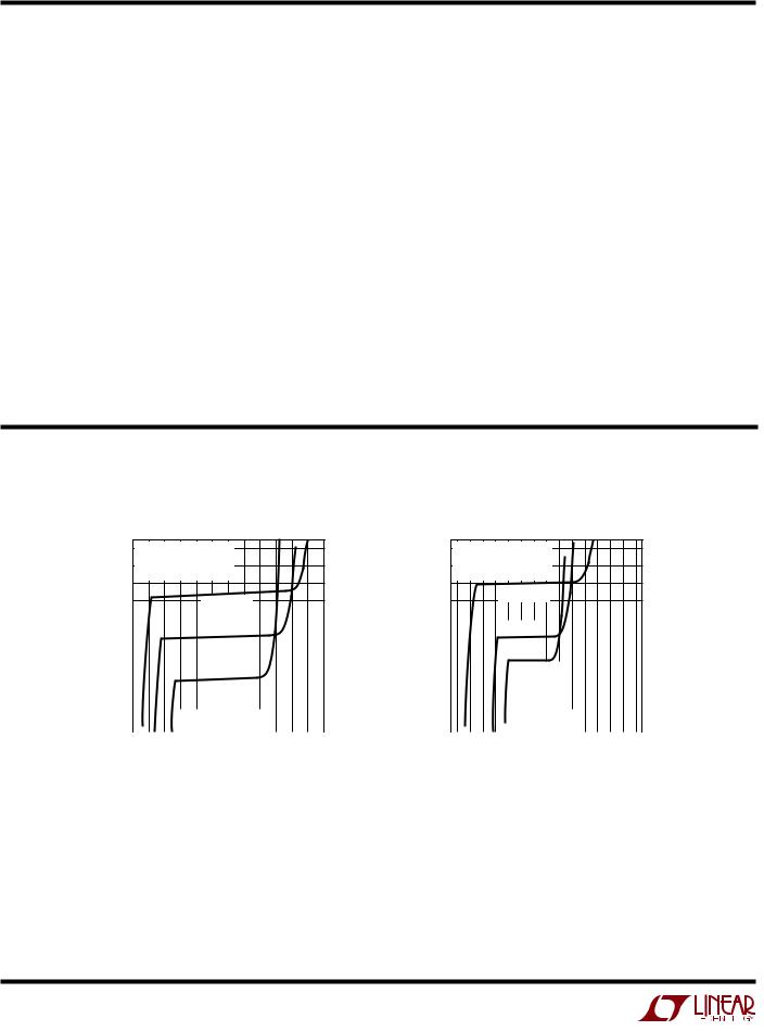
Midscale Output Voltage vs Load Current
3 VREF = VCC
2.9CODE = 128 (LTC1665) CODE = 512 (LTC1660)
2.8
2.7VCC = 5.5V
2.6 |
|
|
|
|
|
|
|
|
|
|
|
|
|
|
|
|
|
|
|
|
|
|
|
|
|
|
|
VCC = 5V |
|
|
|
|
|
|
|
||||
2.5 |
|
|
|
|
|
|
|
|
|
|
|
|
|
|
|
||||
|
|
|
|
|
|
|
|
|
|
|
|
|
|
|
|
|
|
|
|
2.4 |
|
|
|
|
|
|
|
|
|
|
|
|
|
|
|
|
|
|
|
|
|
|
|
|
|
|
|
|
|
|
|
|
|
|
|
|
|
|
|
2.3 |
|
|
|
|
|
|
|
|
|
|
|
|
|
|
|
|
|
|
|
|
|
|
|
|
|
|
|
VCC = 4.5V |
|
|
|
|
|||||||
|
|
|
|
|
|
|
|
|
|
|
|
||||||||
2.2 |
|
|
|
|
|
|
|
|
|
|
|
|
|
|
|
|
|
|
|
|
|
|
|
|
|
|
|
|
|
|
|
|
|
|
|
|
|
|
|
2.1 |
|
|
|
|
|
|
|
|
|
|
|
|
|
|
|
|
|
|
|
|
|
|
|
|
|
|
|
|
|
|
|
|
|
|
|
|
|
|
|
2 |
|
|
SOURCE |
|
|
SINK |
|
|
|
||||||||||
|
|
|
|
|
|
|
|
|
|
|
|
|
|
|
|
|
|
|
|
|
|
|
|
|
|
|
|
|
|
|
|
|
|
|
|
|
|
|
|
–30 |
–20 |
|
|
–10 |
0 |
10 |
20 |
30 |
|||||||||||
|
|
|
|
|
|
|
|
|
IOUT (mA) |
|
|
|
|||||||
VOUT (V)
Midscale Output Voltage vs Load Current
2 VREF = VCC
1.9CODE = 128 (LTC1665)
CODE = 512 (LTC1660)
1.8
1.7VCC = 3.6V
1.6 |
|
|
|
|
|
|
|
|
|
|
|
|
|
|
|
|
|
|
|
VCC = 3V |
|
|
|
|
|
|
|
|
|
|
|||||
1.5 |
|
|
|
|
|
|
|
|
|
|
|
|
|||||
|
|
|
|
|
|
|
|
|
|
|
|
|
|
|
|
|
|
1.4 |
|
|
|
|
|
|
|
|
|
|
|
|
|
|
|
|
|
|
|
|
|
|
|
|
|
|
|
|
|
|
|
|
|
|
|
1.3 |
|
|
|
|
VCC = 2.7V |
|
|
|
|
||||||||
|
|
|
|
|
|
|
|
||||||||||
1.2 |
|
|
|
|
|
|
|
|
|
|
|
|
|
|
|
|
|
|
|
|
|
|
|
|
|
|
|
|
|
|
|
|
|
|
|
1.1 |
|
|
|
|
|
|
|
|
|
|
|
|
|
|
|
|
|
|
|
|
|
|
|
|
|
|
|
|
|
|
|
|
|
|
|
1 |
|
|
|
SOURCE |
|
|
SINK |
|
|
|
|||||||
|
|
|
|
|
|
|
|
|
|
|
|
|
|
|
|
|
|
|
|
|
|
|
|
|
|
|
|
|
|
|
|
|
|
|
|
–15 –12 – 8 |
|
|
– 4 |
0 |
4 |
8 |
12 15 |
||||||||||
|
|
|
|
|
|
IOUT (mA) |
|
|
|
||||||||
1665/60 G01 |
1665/60 G02 |
4
|
|
LTC1665/LTC1660 |
|
|
|
TYPICAL PERFOR A CE CHARACTERISTICS |
(LTC1665/LTC1660) |
|
UW |
|
|
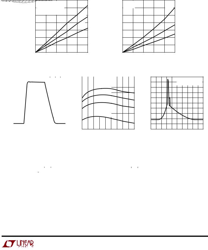
Minimum Supply Headroom vs |
Minimum VOUT vs |
|
Load Current (Output Sourcing) |
Load Current (Output Sinking) |
|
|
1400 |
VREF = 4.096V |
|
|
|
|
|
|
|
|
|
|
|
||
|
1200 |
VOUT < 1LSB |
|
|
|
|
|
|
|
CODE = 255 (LTC1665) |
|
|
|
||
|
1000 |
CODE = 1023 (LTC1660) |
|
|
125°C |
||
(mV) |
|
|
|
|
|
||
800 |
|
|
|
|
|
|
|
OUT |
|
|
|
|
|
25°C |
|
|
|
|
|
|
|
||
|
|
|
|
|
|
|
|
– V |
600 |
|
|
|
|
|
|
CC |
|
|
|
|
|
|
–55°C |
V |
|
|
|
|
|
|
|
|
400 |
|
|
|
|
|
|
|
200 |
|
|
|
|
|
|
|
0 |
|
|
|
|
|
|
|
0 |
2 |
|
4 |
6 |
8 |
10 |
|
|
|
|IOUT| (mA) (Sourcing) |
|
|
||
|
1400 |
VCC = 5V |
|
|
|
|
|
|
|
|
|
|
|
|
1200 |
CODE = 0 |
|
|
|
125°C |
|
|
|
|
|
||
|
1000 |
|
|
|
|
|
(mV) |
800 |
|
|
|
|
25°C |
|
|
|
|
|
||
OUT |
|
|
|
|
|
|
600 |
|
|
|
|
|
|
V |
|
|
|
|
–55°C |
|
|
|
|
|
|
||
|
|
|
|
|
|
|
|
400 |
|
|
|
|
|
|
200 |
|
|
|
|
|
|
0 |
|
|
|
|
|
|
0 |
2 |
4 |
6 |
8 |
10 |
|
|
|
|IOUT| (mA) (Sinking) |
|
|
|
1665/60 G03 |
1665/60 G04 |
VOUT (V)
Large-Signal Step Response
5 |
|
|
|
|
|
|
|
|
|
|
|
|
|
|
|
|
|
|
|
|
|
|
|
|
VCC = VREF = 5V |
|
|
||||||
|
|
|
|
|
|
|
|
|
|
|
||||||
|
|
|
|
|
|
|
|
|
|
|
|
|
|
|
|
|
4 |
|
|
|
|
|
|
|
|
|
10% TO |
|
|
|
|
||
|
|
|
|
|
|
|
|
|
90% STEP |
|
|
|
|
|||
|
|
|
|
|
|
|
|
|
|
|
|
|
||||
3 |
|
|
|
|
|
|
|
|
|
|
|
|
|
|
|
|
|
|
|
|
|
|
|
|
|
|
|
|
|
|
|
|
|
|
|
|
|
|
|
|
|
|
|
|
|
|
|
|
|
|
|
|
|
|
|
|
|
|
|
|
|
|
|
|
|
|
|
2 |
|
|
|
|
|
|
|
|
|
|
|
|
|
|
|
|
|
|
|
|
|
|
|
|
|
|
|
|
|
|
|
|
|
|
|
|
|
|
|
|
|
|
|
|
|
|
|
|
|
|
1 |
|
|
|
|
|
|
|
|
|
|
|
|
|
|
|
|
|
|
|
|
|
|
|
|
|
|
|
|
|
|
|
|
|
|
|
|
|
|
|
|
|
|
|
|
|
|
|
|
|
|
0 |
|
|
|
|
|
|
|
|
|
|
|
|
|
|
|
|
|
|
|
|
|
|
|
|
|
|
|
|
|
|
|
|
|
|
|
|
|
|
|
|
|
|
|
|
|
|
|
|
|
|
0 |
20 |
40 |
60 |
80 |
|
100 |
||||||||||
|
|
|
|
TIME (µs) |
|
|
|
|
|
|
|
|
||||
SUPPLY CURRENT ( A)
Supply Current vs Temperature
500 |
|
|
|
|
|
|
|
|
|
|
|
480 |
|
|
|
|
|
|
|
|
|
|
|
460 |
|
VCC = 5.5V |
|
||
|
|||||
|
|
|
|
|
|
440 |
|
VCC = 4.5V |
|
||
|
|||||
420 |
|
|
|
|
|
|
VCC = 3.6V |
|
|||
400 |
|
|
|||
|
|
|
|
|
|
380 |
|
|
|
|
|
|
|
|
|
|
|
360 |
|
|
|
|
|
|
VCC = 2.7V |
|
|||
|
|
||||
340 |
|
|
|||
|
|
|
|
|
|
|
|
|
|
|
|
320 |
|
|
|
|
|
|
|
|
|
|
|
300 –55 –35 –15 5 25 45 65 85 105 125
TEMPERATURE (°C)
SUPPLY CURRENT (mA)
Supply Current vs Logic Input Voltage
2 


 ALL DIGITAL INPUTS
SHORTED TOGETHER
1.6
1.2
0.8
0.4
0
0 |
1 |
2 |
3 |
4 |
5 |
LOGIC INPUT VOLTAGE (V)
1665/60 G05 1665/60 G06 1665/60 G07
TYPICAL PERFOR A CE CHARACTERISTICS |
(LTC1665) |
UW |
LSB
Integral Nonlinearity (INL) |
|
|
|
|||||||||
1 |
|
|
|
|
|
|
|
|
|
|
|
|
|
VCC = 5V |
|
|
|
|
|
|
|
|
|||
0.8 |
|
|
|
|
|
|
|
|
|
|||
|
VREF = 4.096V |
|
|
|
|
|
|
|
|
|||
|
|
|
|
|
|
|
|
|
||||
0.6 |
|
|
|
|
|
|
|
|
|
|
|
|
|
|
|
|
|
|
|
|
|
|
|
|
|
0.4 |
|
|
|
|
|
|
|
|
|
|
|
|
|
|
|
|
|
|
|
|
|
|
|
|
|
0.2 |
|
|
|
|
|
|
|
|
|
|
|
|
|
|
|
|
|
|
|
|
|
|
|
|
|
0 |
|
|
|
|
|
|
|
|
|
|
|
|
|
|
|
|
|
|
|
|
|
|
|
|
|
–0.2 |
|
|
|
|
|
|
|
|
|
|
|
|
|
|
|
|
|
|
|
|
|
|
|
|
|
–0.4 |
|
|
|
|
|
|
|
|
|
|
|
|
|
|
|
|
|
|
|
|
|
|
|
|
|
–0.6 |
|
|
|
|
|
|
|
|
|
|
|
|
|
|
|
|
|
|
|
|
|
|
|
|
|
–0.8 |
|
|
|
|
|
|
|
|
|
|
|
|
|
|
|
|
|
|
|
|
|
|
|
|
|
–1 |
|
|
|
|
|
|
|
|
|
|
|
|
|
|
|
|
|
|
|
|
|
|
|
|
|
0 |
64 |
|
128 |
192 |
255 |
|||||||
|
|
|
|
|
|
CODE |
|
|
|
|
|
|
|
|
|
|
|
|
|
|
|
|
1665/60 G08 |
||
LSB
Differential Nonlinearity (DNL)
0.5 |
|
|
|
|
|
|
|
|
|
|
|
|
|
VCC = 5V |
|
|
|
|
|
|
|
|
|||
0.4 |
|
|
|
|
|
|
|
|
|
|||
|
VREF = 4.096V |
|
|
|
|
|
|
|
|
|||
|
|
|
|
|
|
|
|
|
||||
0.3 |
|
|
|
|
|
|
|
|
|
|
|
|
|
|
|
|
|
|
|
|
|
|
|
|
|
0.2 |
|
|
|
|
|
|
|
|
|
|
|
|
|
|
|
|
|
|
|
|
|
|
|
|
|
0.1 |
|
|
|
|
|
|
|
|
|
|
|
|
|
|
|
|
|
|
|
|
|
|
|
|
|
0 |
|
|
|
|
|
|
|
|
|
|
|
|
|
|
|
|
|
|
|
|
|
|
|
|
|
–0.1 |
|
|
|
|
|
|
|
|
|
|
|
|
|
|
|
|
|
|
|
|
|
|
|
|
|
–0.2 |
|
|
|
|
|
|
|
|
|
|
|
|
|
|
|
|
|
|
|
|
|
|
|
|
|
–0.3 |
|
|
|
|
|
|
|
|
|
|
|
|
|
|
|
|
|
|
|
|
|
|
|
|
|
–0.4 |
|
|
|
|
|
|
|
|
|
|
|
|
|
|
|
|
|
|
|
|
|
|
|
|
|
–0.5 |
|
|
|
|
|
|
|
|
|
|
|
|
|
|
|
|
|
|
|
|
|
|
|
|
|
0 |
64 |
|
128 |
192 |
255 |
|||||||
|
|
|
|
|
|
CODE |
|
|
|
|
|
|
|
|
|
|
|
|
|
|
|
|
1665/60 G09 |
||
5
 Loading...