


Linear Technology LT1172MK, LT1172MJ8, LT1172IS8, LT1172IN8, LT1172HVCT Datasheet
...LT1170/LT1171/LT1172


 100kHz, 5A, 2.5A and 1.25A High Efficiency Switching Regulators
FEATURES
■Wide Input Voltage Range: 3V to 60V
■Low Quiescent Current: 6mA
■Internal 5A Switch (2.5A for LT1171, 1.25A for LT1172)
■Very Few External Parts Required
■Self-Protected Against Overloads
■Operates in Nearly All Switching Topologies
■Shutdown Mode Draws Only 50μA Supply Current
■Flyback-Regulated Mode Has Fully Floating Outputs
■Comes in Standard 5-Pin Packages
■LT1172 Available in 8-Pin MiniDIP and Surface Mount Packages
■Can Be Externally Synchronized
APPLICATIOUS
■Logic Supply 5V at 10A
■5V Logic to ±15V Op Amp Supply
■Battery Upconverter
■Power Inverter (+ to –) or (– to +)
■Fully Floating Multiple Outputs
USER NOTE:
This data sheet is only intended to provide specifications, graphs, and a general functional description of the LT1170/LT1171/LT1172. Application circuits are included to show the capability of the LT1170/LT1171/LT1172. A complete design manual (AN19) should be obtained to assist in developing new designs. This manual contains a comprehensive discussion of both the LT1070 and the external components used with it, as well as complete formulas for calculating the values of these components. The manual can also be used for the LT1170/LT1171/LT1172 by factoring in the higher frequency. A CAD design program called SwitcherCADTM is also available.
DESCRIPTIOU
The LT®1170/LT1171/LT1172 are monolithic high power switching regulators. They can be operated in all standard switching configurations including buck, boost, flyback, forward, inverting and “Cuk.” A high current, high efficiency switch is included on the die along with all oscillator, control and protection circuitry. Integration of all functions allows the LT1170/LT1171/LT1172 to be built in a standard 5-pin TO-3 or TO-220 power package as well as the 8-pin packages (LT1172). This makes them extremely easy to use and provides “bust proof” operation similar to that obtained with 3-pin linear regulators.
The LT1170/LT1171/LT1172 operate with supply voltages from 3V to 60V, and draw only 6mA quiescent current. They can deliver load power up to 100W with no external power devices. By utilizing current-mode switching techniques, they provide excellent AC and DC load and line regulation.
The LT1170/LT1171/LT1172 have many unique features not found even on the vastly more difficult to use low power control chips presently available. They use adaptive antisat switch drive to allow very wide ranging load currents with no loss in efficiency. An externally activated shutdown mode reduces total supply current to 50μA typically for standby operation.
, LTC and LT are registered trademarks of Linear Technology Corporation.
SwitcherCAD is a trademark of Linear Technology Corporation.
TYPICAL APPLICATIOU
Boost Converter (5V to 12V) Maximum Output Power*
|
5V |
L1** |
L2 |
OUTPUT |
|
|
|
|
|
50mH |
10mH |
FILTER |
|
|
|
|
|
|
|
C3 |
|
|
|
|
|
|
D1 |
100mF |
|
|
|
|
VIN |
|
MBR330 |
|
|
12V |
** |
|
|
|
VSW |
|
|
(W) |
|
|
|
|
+ |
|
R1 |
1A |
|
|
|
|
|
POWER |
|||
+ |
C3* |
|
1000mF |
|
|||
|
|
1% |
|
||||
|
LT1170 |
|
|
C2 |
10.7k |
|
|
|
|
|
|
|
|
||
|
100mF |
|
FB |
|
|
|
|
|
GND |
VC |
|
|
R2 |
|
|
|
|
|
R3 |
|
|
|
|
|
|
|
|
1.24k |
|
|
|
|
|
|
1k |
|
1% |
|
|
|
|
|
C1 |
|
|
|
|
|
|
|
1mF |
|
|
|
|
*REQUIRED IF INPUT LEADS ³ 2" |
** COILTRONICS 50-2-52 |
|
|
|
|||
|
|
|
PULSE ENGINEERING 92114 |
1170/1/2 TA01 |
|
||
|
|
|
|
|
|
||
100 |
|
|
|
|
|
|
|
|
|
|
|
|
|
|
|
|
|
|
|
|
|
|
|
|
|
|
|
|
|
|
|
|
|
80 |
|
LT1170 |
|
|
|
|
|
|
|
|
|
|
|
|
|
|
|
|
|
|
|
|
|
|
|
|
|
|
|||||
|
|
|
|
|
|
|
|
|
|
|
|
|
|
|
|
|
|
|
|
|
|
|
|
|
|
|
|
|
|
|
|
|
|
|
|
|
|
|
|
|
|
|
|
|
|
|
|
|
|
|
|
|
|
|
|
|
|
|
|
|
|
|
|
|
|
||
|
|
|
|
|
|
|
|
|
|
BUCK- |
BOOST |
|
|
|||
|
|
|
|
|
|
|
|
|
|
|
|
|||||
60 |
|
|
|
|
|
|
|
|
|
VO = 30V |
|
|
|
|||
|
|
|
|
|
|
|
|
|
|
|
||||||
|
|
|
|
|
|
|
|
|
|
|
||||||
|
|
|
|
|
|
|
|
|
|
|
|
|||||
|
|
|
BOOST |
|
|
|
|
|
|
|||||||
40 |
|
|
|
|
|
|
|
FLYBACK |
|
|
|
|
|
|
||
|
|
|
|
|
|
|
|
|
|
|
|
|
|
|
|
|
|
|
|
|
|
|
|
|
|
|
|
|
|
|
|
|
|
20 |
|
|
|
|
|
|
|
|
|
|
|
|
|
|
|
|
|
|
|
|
|
|
|
|
|
|
|
|
|
|
|
|
|
|
|
|
|
|
|
|
|
|
|
|
|
|
|
|
|
|
|
|
|
|
|
|
|
|
|
|
|
|
|
|
|
|
|
|
|
|
|
|
|
|
BUCK- |
BOOST |
|
|
|
|||||
|
|
|
|
|
|
|
|
VO = 5V |
|
|
|
|
|
|||
0
0 |
10 |
20 |
30 |
40 |
50 |
INPUT VOLTAGE (V)
* ROUGH GUIDE ONLY. BUCK MODE
POUT = (5A)(VOUT)
SPECIAL TOPOLOGIES DELIVER MORE POWER.
**DIVIDE VERTICAL POWER SCALE BY TWO FOR LT1171, BY FOUR
FOR LT1172.
LT1170/1/2 TA02
1
LT1170/LT1171/LT1172
ABSOLUTE WAXIWUW |
RATIUGS |
|
Supply Voltage |
|
|
LT1170/71/72HV ................................................ |
|
60V |
LT1170/71/72 (See Note 1) ................................ |
|
40V |
Switch Output Voltage |
|
|
LT1170/71/72HV ................................................ |
|
75V |
LT1170/71/72 ..................................................... |
|
65V |
LT1172S8 ........................................................... |
|
60V |
Feedback Pin Voltage (Transient, 1ms) |
................ ±15V |
|
Storage Temperature Range ............... |
|
– 65 ° C to 150°C |
Lead Temperature (Soldering, 10 sec)................. |
300°C |
|
Operating Junction Temperature Range |
– 55 ° C to 150°C |
|
LT1170/71/72M............................... |
|
|
LT1170/71/72HVC, |
|
0 ° C to 100°C |
LT1170/71/72C (Oper.) .................... |
|
|
LT1170/71/72HVC, |
|
0 ° C to 125°C |
LT1170/71/72C (Sh. Ckt.) ................ |
|
|
LT1170/71/72I (Oper.) .................... |
|
– 40 ° C to 100°C |
LT1170/71/72I (Sh. Ckt.)................. |
|
– 40 ° C to 125°C |
Note 1: Minimum effective switch “on” time for the LT1170/71/72 (in current limit only) is ≈ 0.6μs. This limits the maximum safe input voltage during an output shorted condition. Buck mode and inverting mode input voltage during an output shorted condition is limited to:
VIN (max, output shorted) = 15V + |
(R)(IL) + Vf |
||
|
(t)(f) |
|
|
buck and inverting mode |
|
||
|
|
|
|
R = Inductor DC resistance |
|
|
|
IL = 10A for LT1170, 5A for LT1171, and 2.5A for LT1172 Vf = Output catch diode forward voltage at IL
t = 0.6μs, f = 100kHz switching frequency
Maximum input voltage can be increased by increasing R or Vf. External current limiting such as that shown in AN19, Figure 39, will provide protection up to the full supply voltage rating. C1 in Figure 39 should be reduced to 200pF.
Transformer designs will tolerate much higher input voltages because leakage inductance limits rate of rise of current in the switch. These designs must be evaluated individually to assure that current limit is well controlled up to maximum input voltage.
Boost mode designs are never protected against output shorts because the external catch diode and inductor connect input to output.
PACKAGE/ORDER IUFORWATIOU
|
|
|
|
|
|
|
|
TOP VIEW |
|
|
|
|
|
|
|
ORDER PART |
|||
|
|
|
GND |
|
|
|
|
|
|
|
|
|
E2 |
|
|
|
NUMBER |
||
|
|
|
|
1 |
|
|
|
8 |
|
|
|
|
|||||||
|
|
|
|
|
|
|
|
|
|
|
|
|
|
|
|
|
|
|
|
|
|
|
VC |
|
|
|
|
|
|
VSW |
|
|
|
LT1172MJ8 |
|||||
|
|
|
|
2 |
|
|
|
7 |
|
|
|
|
|||||||
|
|
|
|
|
|
|
|
|
|
|
|
|
|
|
|
|
|
|
|
|
|
|
FB |
|
3 |
|
|
|
6 |
|
E1 |
|
|
|
LT1172CJ8 |
||||
|
|
|
|
|
|
|
|
|
|
|
|
|
|
|
|
|
|
|
|
|
|
|
NC* |
|
4 |
|
|
|
5 |
|
VIN |
|
|
|
LT1172CN8 |
||||
|
|
|
|
|
|
|
|
|
|
|
|
|
|
|
|
|
|
|
|
|
|
|
J8 PACKAGE |
N8 PACKAGE |
|
|
|
LT1172IN8 |
|||||||||||
|
|
|
8-LEAD CERDIP |
8-LEAD PDIP |
|
|
|
||||||||||||
|
|
|
|
|
|
LT1172CS8 |
|||||||||||||
|
|
|
S8 PACKAGE, 8-LEAD PLASTIC SO |
|
|
|
|||||||||||||
* Do not connect Pin 4 of the LT1172 DIP or SO to external |
LT1172IS8 |
||||||||||||||||||
|
|||||||||||||||||||
|
circuitry. This pin may be active in future revisions. |
S8 PART MARKING |
|||||||||||||||||
|
|
|
TJMAX = 150°C, θJA = 100°C/W (J) |
|
|
|
|||||||||||||
|
|
|
|
|
|
|
|||||||||||||
|
|
|
TJMAX = 100°C, θJA = 100°C/W (N) |
|
|
|
1172 |
||||||||||||
|
|
|
TJMAX = 100°C, θJA = 120°C/W to 150°C/W |
||||||||||||||||
|
|
|
1172I |
||||||||||||||||
|
|
|
depending on board layout (S) |
|
|
|
|||||||||||||
|
|
|
|
|
|
|
|
|
|
|
|
|
|
|
|
|
|||
|
|
|
|
|
|
|
BOTTOM VIEW |
|
|
|
|
|
|
|
ORDER PART |
||||
|
|
|
VSW |
|
|
|
|
VC |
|
|
|
||||||||
|
|
|
|
|
|
|
|
|
|
NUMBER |
|||||||||
|
|
|
|
1 |
2 |
|
|
|
|
CASE |
|
|
|
||||||
|
|
|
|
|
|
|
|
|
|
|
|
||||||||
|
|
|
|
|
|
|
|
|
|
|
|
|
|
|
|
|
|||
|
|
|
|
|
|
|
|
|
|
|
|
|
|
|
|
||||
|
|
|
|
4 |
3 |
|
|
|
|
IS GND |
|
|
|
LT1170MK |
|||||
|
|
|
|
|
|
|
|
|
|
|
|
|
|
||||||
|
|
|
|
|
|
|
|
|
|
|
|
|
|
|
|
|
|
|
|
|
|
|
VIN |
|
|
|
|
FB |
|
|
|
LT1170CK |
|||||||
|
|
|
K PACKAGE, 4-LEAD TO-3 METAL CAN |
|
|
|
LT1171MK |
||||||||||||
|
|
|
|
|
|
|
|
|
TJMAX |
|
θJC |
θJA |
|||||||
|
|
|
|
|
|
|
|
|
|
LT1171CK |
|||||||||
|
LT1170MK |
|
|
|
|
|
150°C |
2°C/W |
35°C/W |
|
|||||||||
|
LT1170CK |
|
|
|
|
|
100°C |
2°C/W |
35°C/W |
LT1172MK |
|||||||||
|
LT1171MK |
|
|
|
|
|
150°C 4°C/W |
35°C/W |
LT1172CK |
||||||||||
|
LT1171CK |
|
|
|
|
|
100°C |
4°C/W |
35°C/W |
||||||||||
|
LT1172MK |
|
|
|
|
|
150°C |
8°C/W 35°C/W |
|
||||||||||
|
LT1172CK |
|
|
|
|
|
150°C 8°C/W 35°C/W |
|
|||||||||||
|
Based on continuous operation. |
|
|
|
|
|
|
|
|
||||||||||
|
TJMAX = 125°C for intermittent fault conditions. |
|
|
|
|
||||||||||||||
|
|
FRONT VIEW |
*θ will vary from |
|
|
|
ORDER PART |
||||||||||||
|
|
|
|
|
|
|
|
|
approximately 25°C/W with |
||||||||||
|
|
5 |
|
|
|
|
VIN |
NUMBER |
|||||||||||
|
|
4 |
|
|
|
|
VSW |
2.8 sq. in. of 1oz. copper to |
|||||||||||
|
|
|
|
|
|
||||||||||||||
|
3 |
|
|
|
|
GND |
45°C/W with 0.20 sq. in. of |
|
|
||||||||||
|
|
|
|
|
|
|
LT1170CQ |
||||||||||||
|
|
2 |
|
|
|
|
FB |
1oz. copper. Somewhat |
|||||||||||
|
|
1 |
|
|
|
|
VC |
||||||||||||
|
|
|
|
|
lower values can be |
|
|
|
LT1171CQ |
||||||||||
|
|
|
|
|
|
|
|||||||||||||
|
Q PACKAGE, 5-LEAD DD |
obtained with additional |
|||||||||||||||||
|
LT1172CQ |
||||||||||||||||||
TJMAX = 100°C, θJA = *°C/W |
copper layers in multilayer |
||||||||||||||||||
|
|
|
|
|
|
|
|
|
boards. |
|
|
|
|
|
|
|
|
||
|
|
|
|
|
|
|
|
|
|
|
|
|
|
|
|
|
|
||
|
|
|
|
|
|
|
|
TOP VIEW |
|
|
|
|
|
|
|
ORDER PART |
|||
|
|
|
|
|
|
|
|
|
|
|
|
|
|
|
|
|
|
|
|
|
|
|
|
|
|
|
|
|
|
|
|
|
|
|
|
|
|
|
|
|
|
|
NC |
1 |
|
|
|
|
|
|
16 |
|
NC |
|
|
|
NUMBER |
||
|
|
|
|
|
|
|
|
|
|
|
|
|
|
|
|
|
|
|
|
|
|
|
NC |
2 |
|
|
|
|
|
|
15 |
|
NC |
|
|
|
|
||
|
|
|
|
|
|
|
|
|
|
|
|
|
|
||||||
|
|
|
|
|
|
|
|
|
|
|
|
|
|
|
|
|
|
||
|
|
|
GND |
3 |
|
|
|
|
|
|
14 |
|
E2 |
|
|
|
LT1172CSW |
||
|
|
|
|
|
|
|
|
|
|
|
|
|
|
|
|
|
|
|
|
|
|
|
VC |
4 |
|
|
|
|
|
|
13 |
|
VSW |
|
|
|
|||
|
|
|
|
|
|
|
|
|
|
|
|
|
|
||||||
|
|
|
|
|
|
|
|
|
|
|
|
|
|
|
|
|
|
||
|
|
|
FB |
5 |
|
|
|
|
|
|
12 |
|
E1 |
|
|
|
|
||
|
|
|
|
|
|
|
|
|
|
|
|
|
|
|
|
|
|
||
|
|
|
NC |
6 |
|
|
|
|
|
|
11 |
|
VIN |
|
|
|
|
||
|
|
|
|
|
|
|
|
|
|
|
|
|
|
|
|
|
|
||
|
|
|
NC |
7 |
|
|
|
|
|
|
10 |
|
NC |
|
|
|
|
||
|
|
|
|
|
|
|
|
|
|
|
|
|
|
|
|
|
|
||
|
|
|
NC |
8 |
|
|
|
|
|
|
9 |
|
NC |
|
|
|
|
||
|
|
|
|
|
|
|
|
|
|
|
|
|
|
|
|
||||
|
|
|
SW PACKAGE, 16-LEAD PLASTIC SO WIDE |
|
|
|
|
||||||||||||
|
|
|
TJMAX = 100°C, θJA = 150°C/W |
|
|
|
|
||||||||||||
|
Based on continuous operation. |
|
|
|
|
|
|
|
|
||||||||||
|
TJMAX = 125°C for intermittent fault conditions. |
|
|||||||||||||||||
|
|
|
|
|
|
|
|
FRONT VIEW |
|
|
|
|
|
|
|
ORDER PART |
|||
|
|
|
|
|
|
|
|
|
|
|
|
|
|
|
NUMBER |
||||
|
|
|
|
|
5 |
|
|
|
|
|
|
VIN |
|
|
|
||||
|
|
|
|
|
|
|
|
|
|
|
|
|
|
||||||
|
|
|
|
|
|
|
|
|
|
|
|
|
|
|
|||||
|
|
|
|
|
4 |
|
|
|
|
|
|
VSW |
|
LT1170CT |
|||||
|
|
|
|
|
|
|
|
|
|
|
|||||||||
|
|
|
|
|
3 |
|
|
|
|
|
|
GND |
|||||||
|
|
|
|
|
|
|
|
|
|
|
|||||||||
|
|
|
|
|
2 |
|
|
|
|
|
|
FB |
|
|
|
LT1170IT |
|||
|
|
|
|
|
1 |
|
|
|
|
|
|
VC |
|
|
|
||||
|
|
|
|
|
|
|
|
|
|
|
|
|
|
||||||
|
|
|
|
|
|
|
|
|
|
|
|
|
|
||||||
|
|
|
|
T PACKAGE, 5-LEAD TO-220 |
|
|
|
LT1170HVCT |
|||||||||||
|
|
|
|
|
|
|
|
|
|
|
|
|
|
|
|
|
|
|
LT1170HVIT |
|
|
|
|
|
|
|
|
|
TJMAX |
|
θJC |
θJA |
|
|
LT1171CT |
||||
|
LT1170CT/LT1170HVCT |
100°C |
2°C/W |
75°C/W |
|||||||||||||||
|
LT1171IT |
||||||||||||||||||
|
LT1171CT/LT1171HVCT |
° |
|
|
° |
|
° |
|
|
||||||||||
|
100 C |
4 C/W |
75 C/W |
LT1171HVCT |
|||||||||||||||
|
LT1172CT/LT1172HVCT |
100°C |
8°C/W |
75°C/W |
|||||||||||||||
|
Based on continuous operation. |
|
|
|
|
|
|
|
LT1172CT |
||||||||||
|
TJMAX = 125°C for intermittent fault conditions. |
|
|
|
LT1172HVCT |
||||||||||||||
|
|
|
|
|
|
|
|
|
|
|
|
|
|
|
|
|
|
|
|
|
|
|
|
|
|
|
|
|
|
|
|
|
|
|
|
|
|
|
|
2

LT1170/LT1171/LT1172
ELECTRICAL CHARACTERISTICS VIN = 15V, VC = 0.5V, VFB = VREF, output pin open, unless otherwise noted.
SYMBOL |
PARAMETER |
CONDITIONS |
|
|
MIN |
TYP |
MAX |
UNITS |
||
VREF |
Reference Voltage |
Measured at Feedback Pin |
|
1.224 |
1.244 |
1.264 |
V |
|||
|
|
|
VC = 0.8V |
|
● |
1.214 |
1.244 |
1.274 |
V |
|
IB |
Feedback Input Current |
VFB = VREF |
|
|
|
350 |
750 |
nA |
||
|
|
|
|
|
|
● |
|
|
1100 |
nA |
gm |
Error Amplifier |
DIC = ±25mA |
|
|
3000 |
4400 |
6000 |
mmho |
||
|
Transconductance |
|
|
|
● |
2400 |
|
7000 |
mmho |
|
|
Error Amplifier Source or |
VC = 1.5V |
|
|
150 |
200 |
350 |
mA |
||
|
Sink Current |
|
|
|
● |
120 |
|
400 |
mA |
|
|
Error Amplifier Clamp |
Hi Clamp, VFB = 1V |
|
|
1.80 |
|
2.30 |
V |
||
|
Voltage |
Lo Clamp, VFB = 1.5V |
|
|
0.25 |
0.38 |
0.52 |
V |
||
|
Reference Voltage Line |
3V £ VIN £ VMAX |
|
● |
|
|
0.03 |
%/V |
||
|
Regulation |
VC = 0.8V |
|
|
|
|
|
|
||
AV |
Error Amplifier Voltage Gain |
0.9V £ VC £ 1.4V |
|
|
500 |
800 |
|
V/V |
||
|
Minimum Input Voltage (Note 3) |
|
|
|
● |
|
2.6 |
3.0 |
V |
|
|
|
|
|
|
|
|
|
|
|
|
IQ |
Supply Current |
3V £ VIN £ VMAX, VC = 0.6V |
|
|
6 |
9 |
mA |
|||
|
Control Pin Threshold |
Duty Cycle = 0 |
|
|
0.8 |
0.9 |
1.08 |
V |
||
|
|
|
|
|
|
● |
0.6 |
|
1.25 |
V |
|
Normal/Flyback Threshold |
|
|
|
|
0.4 |
0.45 |
0.54 |
V |
|
|
on Feedback Pin |
|
|
|
|
|
|
|
|
|
VFB |
Flyback Reference Voltage |
IFB = 50mA |
|
|
15.0 |
16.3 |
17.6 |
V |
||
|
(Note 3) |
|
|
|
● |
14.0 |
|
18.0 |
V |
|
|
Change in Flyback Reference |
0.05 £ IFB £ 1mA |
|
|
4.5 |
6.8 |
9 |
V |
||
|
Voltage |
|
|
|
|
|
|
|
|
|
|
Flyback Reference Voltage |
IFB = 50mA |
|
|
|
0.01 |
0.03 |
%/V |
||
|
Line Regulation (Note 3) |
7V £ VIN £ VMAX |
|
|
|
|
|
|
||
|
Flyback Amplifier |
DIC = ±10mA |
|
|
150 |
300 |
650 |
mmho |
||
|
Transconductance (gm) |
|
|
|
|
|
|
|
|
|
|
Flyback Amplifier Source |
VC = 0.6V |
Source |
● |
15 |
32 |
70 |
mA |
||
|
and Sink Current |
IFB = 50mA |
Sink |
● |
25 |
40 |
70 |
mA |
||
BV |
Output Switch Breakdown |
3V £ VIN £ VMAX, |
|
LT1170/LT1171/LT1172 |
● |
65 |
90 |
|
V |
|
|
Voltage |
ISW = 1.5mA |
|
LT1170HV/LT1171HV/LT1172HV |
● |
75 |
90 |
|
V |
|
|
|
|
|
|
LT1172S8 |
● |
60 |
80 |
|
V |
VSAT |
Output Switch |
LT1170 |
|
● |
|
0.15 |
0.24 |
W |
||
|
“On” Resistance (Note 1) |
LT1171 |
|
● |
|
0.30 |
0.50 |
W |
||
|
|
|
LT1172 |
|
● |
|
0.60 |
1.00 |
W |
|
|
Control Voltage to Switch |
LT1170 |
|
|
|
8 |
|
A/V |
||
|
Current Transconductance |
LT1171 |
|
|
|
4 |
|
A/V |
||
|
|
|
LT1172 |
|
|
|
2 |
|
A/V |
|
|
|
|
|
|
|
|
|
|
|
|
ILIM |
Switch Current Limit |
(LT1170) |
Duty Cycle = 50% |
TJ ³ 25°C |
● |
5 |
|
10 |
A |
|
|
|
|
Duty Cycle = 50% |
TJ < 25°C |
● |
5 |
|
11 |
A |
|
|
|
|
Duty Cycle = 80% (Note 2) |
● |
4 |
|
10 |
A |
||
|
|
(LT1171) |
Duty Cycle = 50% |
TJ ³ 25°C |
● |
2.5 |
|
5.0 |
A |
|
|
|
|
Duty Cycle = 50% |
TJ < 25°C |
● |
2.5 |
|
5.5 |
A |
|
|
|
|
Duty Cycle = 80% (Note 2) |
● |
2.0 |
|
5.0 |
A |
||
|
|
(LT1172) |
Duty Cycle = 50% |
TJ ³ 25°C |
● |
1.25 |
|
3.0 |
A |
|
|
|
|
Duty Cycle = 50% |
TJ < 25°C |
● |
1.25 |
|
3.5 |
A |
|
|
|
|
Duty Cycle = 80% (Note 2) |
● |
1.00 |
|
2.5 |
A |
||
3

LT1170/LT1171/LT1172
ELECTRICAL CHARACTERISTICS VIN = 15V, VC = 0.5V, VFB = VREF, output pin open, unless otherwise noted.
SYMBOL |
PARAMETER |
CONDITIONS |
MIN |
TYP |
MAX |
UNITS |
||
|
|
|
|
|
|
|
|
|
IIN |
Supply Current Increase |
|
|
|
25 |
35 |
mA/A |
|
ISW |
|
During Switch On-Time |
|
|
|
|
|
|
f |
Switching Frequency |
|
|
88 |
100 |
112 |
kHz |
|
|
|
|
|
● |
85 |
|
115 |
kHz |
|
|
|
|
|
|
|
|
|
DCMAX |
Maximum Switch Duty Cycle |
|
● |
85 |
92 |
97 |
% |
|
|
|
Shutdown Mode |
3V ≤ VIN ≤ VMAX |
|
|
100 |
250 |
μA |
|
|
Supply Current |
VC = 0.05V |
|
|
|
|
|
|
|
Shutdown Mode |
3V ≤ VIN ≤ VMAX |
|
100 |
150 |
250 |
mV |
|
|
Threshold Voltage |
|
● |
50 |
|
300 |
mV |
|
|
Flyback Sense Delay Time (Note 3) |
|
|
|
1.5 |
|
μs |
|
|
|
|
|
|
|
|
|
The ● denotes the specifications which apply over the full operating temperature range.
VMAX = 40V for LT1170/71/72 and 60V for LT1170/71/72HV.
Note 1: Measured with VC in hi clamp, VFB = 0.8V. ISW = 4A for LT1170, 2A for LT1171, and 1A for LT1172.
Note 2: For duty cycles (DC) between 50% and 80%, minimum
guaranteed switch current is given by ILIM = 3.33 (2 – DC) for the LT1170,
ILIM = 1.67 (2 – DC) for the LT1171, and ILIM = 0.833 (2 – DC) for the LT1172.
Note 3: Minimum input voltage for isolated flyback mode is 7V. VMAX = 55V for HV grade in fully isolated mode to avoid switch breakdown.
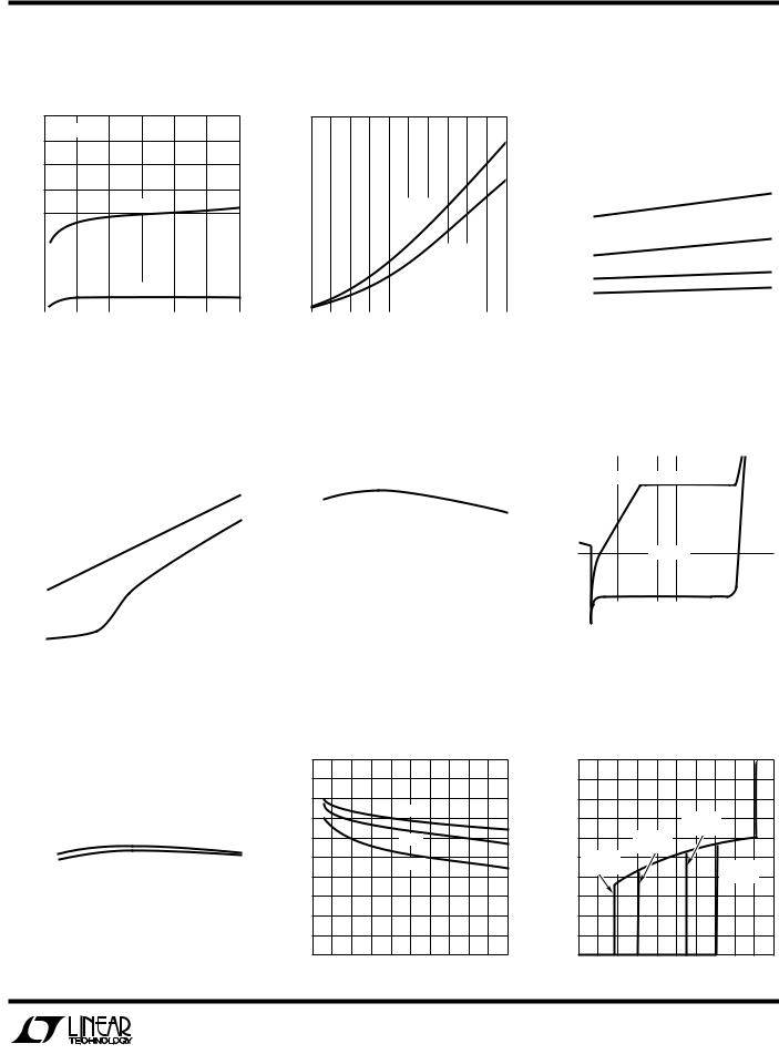
TYPICAL PERFORWAUCE CHARACTERISTICS
Switch Current Limit vs Duty Cycle*
|
16 |
|
(A) |
12 |
|
|
|
|
CURRENT |
–55°C |
25°C |
|
||
8 |
|
|
|
|
|
SWITCH |
125°C |
|
4 |
|
|
|
|
*DIVIDE VERTICAL SCALE BY TWO FOR LT1171, BY FOUR FOR LT1172.
0 


 0 10 20 30 40 50 60 70 80 90 100
DUTY CYCLE (%)
1170/1/2 G01
MINIMUM INPUT VOLTAGE (V)
Minimum Input Voltage
2.9
SWITCH CURRENT = IMAX
2.8
2.7
2.6
SWITCH CURRENT = 0A
2.5
2.4
2.3 |
|
|
|
|
|
100 |
|
|
–75 –50 |
–25 |
0 |
25 |
50 |
75 |
125 |
150 |
TEMPERATURE (°C)
1170/1/2 G02
SWITCH SATURATION VOLTAGE (V)
Switch Saturation Voltage
1.6
1.4
150°C
1.2
100°C
1.0
25°C
0.8
–55°C
0.6
0.4
0.2* DIVIDE CURRENT BY TWO FOR LT1171, BY FOUR FOR LT1172.
0
0 |
1 |
2 |
3 |
4 |
5 |
6 |
7 |
8 |
SWITCH CURRENT (A)*
1170/1/2 G03
Line Regulation |
|
Feedback Bias Current vs |
Reference Voltage vs Temperature |
Temperature |
|
5 |
|
|
|
|
|
|
|
1.250 |
|
|
|
|
|
|
|
|
|
|
800 |
|
|
|
|
|
|
|
|
|
REFERENCE VOLTAGE CHANGE (mV) |
4 |
|
|
|
|
|
|
|
1.248 |
|
|
|
|
|
|
|
|
|
|
700 |
|
|
|
|
|
|
|
|
|
|
|
|
|
|
|
|
|
|
|
|
|
|
|
|
|
|
FEEDBACK BIAS CURRENT (nA) |
|
|
|
|
|
|
|
|
|
|||
3 |
|
|
|
TJ = 150°C |
|
REFERENCE VOLTAGE (V) |
1.246 |
|
|
|
|
|
|
|
|
|
600 |
|
|
|
|
|
|
|
|
|
|||
2 |
|
|
|
|
|
|
|
|
|
|
|
|
|
|
|
|
|
|
|
|
|
|
|||||||
|
|
|
|
|
|
|
|
|
|
|
|
|
|
|
|
|
|
|
|
|
|
|
|
|
|
||||
1 |
|
|
|
|
|
|
1.244 |
|
|
|
|
|
|
|
|
|
500 |
|
|
|
|
|
|
|
|
|
|||
|
|
|
|
|
|
|
|
|
|
|
|
|
|
|
|
|
|
|
|
|
|
|
|
|
|
||||
0 |
TJ = –55°C |
|
|
|
TJ = 25°C |
|
1.242 |
|
|
|
|
|
|
|
|
|
400 |
|
|
|
|
|
|
|
|
|
|||
–1 |
|
|
|
|
|
|
|
|
|
|
|
|
|
|
|
|
|
|
|
|
|
|
|
|
|
||||
|
|
|
|
|
|
1.240 |
|
|
|
|
|
|
|
|
|
300 |
|
|
|
|
|
|
|
|
|
||||
|
|
|
|
|
|
|
|
|
|
|
|
|
|
|
|
|
|
|
|
|
|
|
|
|
|||||
–2 |
|
|
|
|
|
|
1.238 |
|
|
|
|
|
|
|
|
|
200 |
|
|
|
|
|
|
|
|
|
|||
–3 |
|
|
|
|
|
|
|
|
|
|
|
|
|
|
|
|
|
|
|
|
|
|
|
|
|||||
|
|
|
|
|
|
|
|
|
|
|
|
|
|
|
|
|
|
|
|
|
|
|
|
|
|
||||
–4 |
|
|
|
|
|
|
1.236 |
|
|
|
|
|
|
|
|
|
100 |
|
|
|
|
|
|
|
|
|
|||
|
|
|
|
|
|
|
|
|
|
|
|
|
|
|
|
|
|
|
|
|
|
|
|
|
|
|
|
|
|
|
–5 |
|
|
|
|
|
|
|
1.234 |
–50 |
|
0 |
|
|
|
100 |
125 |
|
|
0 |
–50 |
|
0 |
|
|
|
100 |
125 |
|
|
0 |
10 |
20 |
30 |
40 |
50 |
60 |
|
–75 |
–25 |
25 |
50 |
75 |
150 |
|
–75 |
–25 |
25 |
50 |
75 |
150 |
||||||||
INPUT VOLTAGE (V) |
|
TEMPERATURE (°C) |
TEMPERATURE (°C) |
|
1170/1/2 G04 |
1170/1/2 G05 |
1170/1/2 G06 |
|
|
||
|
|
|
|
|
|
|
|
4
LT1170/LT1171/LT1172
TYPICAL PERFORWAUCE CHARACTERISTICS
SUPPLY CURRENT (μA)
Supply Current vs Supply Voltage (Shutdown Mode)
160
TJ = 25°C
140
120
100
VC = 50mV
80
60 |
|
|
|
|
|
|
|
|
|
|
|
|
|
|
|
|
|
|
|
40 |
|
|
|
|
|
|
|
|
|
|
|
|
|
|
|
|
|
|
|
20 |
|
|
|
|
|
|
|
|
|
|
|
|
VC = 0V |
|
|
|
|
||
|
|
|
|
|
|
|
|||
0 |
|
|
|
|
|
|
|
|
|
|
10 |
20 |
30 |
40 |
50 |
|
|
||
0 |
60 |
||||||||
|
|
|
SUPPLY VOLTAGE (V) |
|
|
|
|||
|
|
|
|
|
|
|
1170/1/2 G07 |
||
Driver Current* vs Switch Current
160
|
140 |
|
|
|
|
|
|
|
|
|
|
|
|
|
|
|
|
|
|
|
|
|
|
|
|
|
|
|
|
(mA) |
120 |
|
|
|
|
|
|
|
|
|
|
|
|
|
|
|
|
|
|
|
|
|
|
|
|
|
|
||
100 |
|
|
|
|
|
|
|
|
|
|
|
|
|
|
CURRENT |
|
|
|
|
|
|
|
|
|
|
|
|
|
|
|
|
|
|
|
|
|
|
|
|
|
|
|
||
80 |
|
|
|
TJ = –55°C |
|
|
|
|
|
|||||
DRIVER |
|
|
|
|
|
|
|
|
|
|
|
|
|
|
60 |
|
|
|
|
|
|
|
|
|
|
|
|
|
|
|
|
|
|
|
|
|
|
|
|
|
|
|
|
|
|
40 |
|
|
|
|
|
|
|
TJ = ³ 25°C |
|
|
|||
|
|
|
|
|
|
|
|
|
|
|
|
|
|
|
|
|
|
|
|
|
|
|
|
|
|
|
|
|
|
|
20 |
|
|
|
|
|
|
|
|
|
|
|
|
|
|
|
|
|
|
|
|
|
|
|
|
|
|
|
|
|
0 |
|
|
|
|
|
|
|
|
|
|
|
|
|
|
|
1 |
2 |
3 |
4 |
|
|
|||||||
|
0 |
5 |
||||||||||||
SWITCH CURRENT (A)
1170/1/2 G08
*AVERAGE LT1170 POWER SUPPLY CURRENT IS FOUND BY MULTIPLYING DRIVER CURRENT BY DUTY CYCLE, THEN ADDING QUIESCENT CURRENT.
Supply Current vs Input Voltage*
|
15 |
|
|
|
|
|
|
|
|
|
|
|
|
|
|
|
|
|
|
|
|
|
|
|
|
|
|
|
|
|
|
|
|
|
|
|
|
|
14 |
|
|
TJ = |
25°C |
|
|
|
|
|
|
|
|
|
|
|
|
|
|
13 |
|
|
NOTE THAT THIS CURRENT DOES NOT |
|
|
|
|
||||||||||
(mA) |
|
|
INCLUDE DRIVER CURRENT, WHICH IS |
|
|
|
|
|||||||||||
12 |
|
|
|
|
|
|
||||||||||||
|
|
A FUNCTION OF LOAD CURRENT AND |
|
|
|
|
||||||||||||
|
|
|
|
|
|
|
||||||||||||
CURRENT |
11 |
|
|
DUTY CYCLE. |
|
|
|
|
|
|
|
|
|
|
|
|||
|
|
|
|
|
|
|
|
|
|
|
|
|
|
|
|
|
|
|
|
10 |
|
|
|
|
|
|
|
|
90% |
DUTY |
CYCLE |
|
|
||||
|
|
|
|
|
|
|
|
|
|
|
||||||||
|
|
|
|
|
|
|
|
|
|
|
|
|
|
|
|
|
|
|
|
|
|
|
|
|
|
|
|
|
|
|
|
|
|
||||
SUPPLY |
9 |
|
|
|
|
|
|
|
|
50% |
DUTY |
CYCLE |
|
|
||||
|
|
|
|
|
|
|
|
|
|
|||||||||
8 |
|
|
|
|
|
|
|
|
|
|
|
|
|
|
|
|
|
|
|
|
|
|
|
|
|
|
|
|
|
|
|
|
|
|
|
||
|
|
|
|
|
|
|
|
|
|
|
|
|
|
|
|
|
|
|
|
7 |
|
|
|
|
|
|
|
|
10% |
DUTY |
CYCLE |
|
|
|
|||
|
6 |
|
|
|
|
|
|
|
|
|
|
|
|
|
|
|
|
|
|
|
|
|
|
|
|
|
|
|
0% DUTY CYCLE |
|
|
|
|||||
|
|
|
|
|
|
|
|
|
|
|
|
|
||||||
|
|
|
|
|
|
|
|
|
|
|
|
|
|
|||||
|
5 |
|
|
|
|
|
|
|
|
|
|
|
|
|
|
|
|
|
|
|
|
|
|
|
|
|
|
|
|
|
|
|
|
|
60 |
||
|
0 |
|
10 |
20 |
30 |
40 |
50 |
|
|
|||||||||
|
|
|
|
|
|
INPUT VOLTAGE (V) |
|
1170/1/2 G09 |
||||||||||
*UNDER VERY LOW OUTPUT CURRENT CONDITIONS, DUTY CYCLE FOR MOST CIRCUITS WILL APPROACH
10% OR LESS.
SUPPLY CURRENT (μA)
Shutdown Mode Supply Current
200 |
|
|
|
|
|
|
|
|
|
|
|
|
|
|
|
|
|
|
|
|
|
|
|
|
|
|
|
|
|
|
|
|
|
|
|
|
|
|
|
|
|
|
|
|
|
180 |
|
|
|
|
|
|
|
|
|
|
|
|
|
|
|
|
|
|
|
|
|
|
|
|
|
|
|
|
|
|
|
|
|
|
|
|
|
|
|
|
|
|
|
|
|
160 |
|
|
|
|
|
|
|
|
|
|
|
|
|
|
|
|
|
|
|
|
|
|
|
|
|
|
|
|
|
|
|
|
|
|
|
|
|
|
|
|
|
|
|
|
|
140 |
|
|
|
|
|
|
|
|
|
|
|
|
|
|
|
|
|
|
|
|
|
|
|
|
|
|
|
|
|
|
|
|
|
|
|
|
|
|
|
|
|
|
|
|
|
120 |
|
|
|
|
|
|
|
|
TJ = 150°C |
|
|
|
|
|
|
|
|
|
|
|||
|
|
|
|
|
|
|
|
|
|
|
|
|
|
|
|
|
|
|||||
100 |
|
|
|
|
|
|
|
|
|
|
|
|
|
|
|
|
|
|
|
|
|
|
|
|
|
|
|
|
|
|
|
|
|
|
|
|
|
|
|
|
|
|
|
|
|
|
|
|
|
|
|
|
|
|
|
|
|
|
|
|
|
|
|
|
|
|
|
|
80 |
|
|
|
|
|
|
|
|
|
|
|
|
|
|
|
|
|
|
|
|
|
|
|
|
|
|
|
|
|
|
|
|
|
|
|
|
|
|
|
|
|
|
|
|
|
60 |
|
|
|
|
|
|
|
|
|
|
|
|
|
|
|
|
|
|
|
|
|
|
|
|
|
|
|
|
|
|
|
–55°C £ TJ £ 125°C |
|
|
|
|
|||||||||
40 |
|
|
|
|
|
|
|
|
|
|
|
|
|
|||||||||
|
|
|
|
|
|
|
|
|
|
|
|
|
|
|
|
|
|
|
|
|
|
|
|
|
|
|
|
|
|
|
|
|
|
|
|
|
|
|
|
|
|
|
|
|
|
20 |
|
|
|
|
|
|
|
|
|
|
|
|
|
|
|
|
|
|
|
|
|
|
|
|
|
|
|
|
|
|
|
|
|
|
|
|
|
|
|
|
|
|
|
|
|
0 |
|
|
|
|
|
|
|
|
|
|
|
|
|
|
|
|
|
|
|
|
|
|
|
10 |
|
|
30 |
40 |
|
|
|
|
|
|
|
|
|
|
|
|
|||||
0 |
20 |
50 |
60 |
70 |
80 |
90 |
100 |
|||||||||||||||
VC PIN VOLTAGE (mV)
1170/1/2 G10
Error Amplifier Transconductance
|
5000 |
|
|
|
|
|
|
|
|
|
|
|
|
|
|
|
|
|
|
|
|
|
|
|
|
|
|
|
|
|
|
|
|
|
|
|
|
|
|
|
|
|
4500 |
|
|
|
|
|
|
|
|
|
|
|
gm = |
DI |
(VC PIN) |
|
|
|||
mho)(μ |
|
|
|
|
|
|
|
|
|
|
|
DV (FB PIN) |
|
|
||||||
|
|
|
|
|
|
|
|
|
|
|
|
|
|
|
|
|||||
3500 |
|
|
|
|
|
|
|
|
|
|
|
|
|
|
|
|
|
|
|
|
TRANSCONDUCTANCE |
4000 |
|
|
|
|
|
|
|
|
|
|
|
|
|
|
|
|
|
|
|
|
|
|
|
|
|
|
|
|
|
|
|
|
|
|
|
|
|
|
||
1000 |
|
|
|
|
|
|
|
|
|
|
|
|
|
|
|
|
|
|
|
|
|
|
|
|
|
|
|
|
|
|
|
|
|
|
|
|
|
|
|
||
|
3000 |
|
|
|
|
|
|
|
|
|
|
|
|
|
|
|
|
|
|
|
|
|
|
|
|
|
|
|
|
|
|
|
|
|
|
|
|
|
|
|
|
|
2500 |
|
|
|
|
|
|
|
|
|
|
|
|
|
|
|
|
|
|
|
|
|
|
|
|
|
|
|
|
|
|
|
|
|
|
|
|
|
|
|
|
|
2000 |
|
|
|
|
|
|
|
|
|
|
|
|
|
|
|
|
|
|
|
|
|
|
|
|
|
|
|
|
|
|
|
|
|
|
|
|
|
|
|
|
|
1500 |
|
|
|
|
|
|
|
|
|
|
|
|
|
|
|
|
|
|
|
|
|
|
|
|
|
|
|
|
|
|
|
|
|
|
|
|
|
|
|
|
|
500 |
|
|
|
|
|
|
|
|
|
|
|
|
|
|
|
|
|
|
|
|
|
|
|
|
|
|
|
|
|
|
|
|
|
|
|
|
|
|
|
|
|
|
|
|
|
|
|
|
|
|
|
|
|
|
|
|
|
|
|
|
|
|
0 |
|
|
|
|
|
|
|
|
|
|
|
|
|
|
|
|
|
|
|
|
|
–50 |
|
|
0 |
|
|
|
|
|
|
100 |
125 |
|
|
|||||
|
–75 |
–25 |
25 |
50 |
75 |
150 |
||||||||||||||
TEMPERATURE (°C)
1170/1/2 G11
VC Pin Characteristics
|
300 |
|
|
|
|
|
|
|
|
|
|
|
|
|
|
|
|
|
|
|
|
|
|
|
|
|
|
|
|
|
|
|
|
|
|
|
|
|
|
|
|
|
|
|
|
||
|
200 |
|
VFB |
= 1.5V |
(CURRENT |
INTO |
VC |
PIN) |
|
|
|
||||
A) |
100 |
|
|
|
|
|
|
|
|
|
|
|
|
|
|
|
|
|
|
|
|
|
|
|
|
|
|
|
|
||
(μ |
|
|
|
|
|
|
|
|
|
|
|
|
|
|
|
CURRENT |
0 |
|
|
|
|
|
|
|
|
|
|
|
|
|
|
|
|
|
|
|
|
TJ = 25°C |
|
|
|
|
|
|
|||
PIN |
–100 |
|
|
|
|
|
|
|
|
|
|
|
|||
|
|
|
|
|
|
|
|
|
|
|
|
|
|
||
|
|
|
|
|
|
|
|
|
|
|
|
|
|
||
|
|
|
|
|
|
|
|
|
|
|
|
|
|
|
|
|
|
|
|
|
|
|
|
|
|
|
|
|
|
|
|
C |
–200 |
|
|
|
|
|
|
|
|
|
|
|
|
|
|
V |
|
|
|
|
|
|
|
|
|
|
|
|
|
|
|
|
–300 |
|
|
VFB = 0.8V (CURRENT OUT OF VC PIN) |
|
|
|||||||||
|
|
|
|
|
|||||||||||
|
|
|
|
|
|
|
|
|
|
|
|
|
|
|
|
|
|
|
|
|
|
|
|
|
|
|
|
|
|
|
|
|
–400 |
|
|
|
|
|
|
|
|
|
|
|
|
|
|
|
|
|
|
|
|
|
|
|
|
|
|
|
|
|
|
|
|
0.5 |
|
|
|
1.5 |
|
|
|
|
|||||
|
0 |
1.0 |
|
2.0 |
2.5 |
||||||||||
VC PIN VOLTAGE (V)
1170/1/2 G12
IDLE SUPPLY CURRENT (mA)
Idle Supply Current vs |
|
|
|
|
|
|
|
|
||||||||||||||||
Temperature |
|
|
|
|
|
|
|
|
|
|
|
|
|
|
||||||||||
11 |
|
|
|
|
|
|
|
|
|
|
|
|
|
|
|
|
|
|
|
|
|
|
|
|
|
|
|
|
|
|
|
|
|
|
|
|
|
|
|
|
|
|
|
|
|
|
|
|
|
10 |
|
|
VC |
= 0.6V |
|
|
|
|
|
|
|
|
|
|
|
|
|
|
|
|
|
|
||
|
|
|
|
|
|
|
|
|
|
|
|
|
|
|
|
|
|
|
|
|
|
|
||
9 |
|
|
|
|
|
|
|
|
|
|
|
|
|
|
|
|
|
|
|
|
|
|
|
|
|
|
|
|
|
|
|
|
|
|
|
|
|
|
|
|
|
|
|
|
|
|
|
|
|
8 |
|
|
|
|
|
|
|
|
|
|
|
|
|
|
|
|
|
|
|
|
|
|
|
|
|
|
|
|
|
|
|
|
|
|
|
|
|
|
|
|
|
|
|
|
|
|
|
|
|
7 |
|
|
|
|
|
|
|
|
|
|
|
|
|
|
|
|
|
|
|
|
||||
|
|
|
|
|
|
|
V |
SUPPLY |
= 60V |
|
|
|
|
|
|
|
|
|
||||||
|
|
|
|
|
|
|
|
|
|
|
|
|
|
|
|
|||||||||
6 |
|
|
|
|
|
|
|
|
|
|
|
|
|
|
|
|
|
|
|
|
|
|
|
|
|
|
|
|
|
|
|
|
VSUPPLY = 3V |
|
|
|
|
|
|
|
|
|
|
||||||
|
|
|
|
|
|
|
|
|
|
|
|
|
|
|
|
|
|
|||||||
|
|
|
|
|
|
|
|
|
|
|
|
|
|
|
|
|
|
|||||||
5 |
|
|
|
|
|
|
|
|
|
|
|
|
|
|
|
|
|
|
|
|
|
|
|
|
|
|
|
|
|
|
|
|
|
|
|
|
|
|
|
|
|
|
|
|
|
|
|
|
|
4 |
|
|
|
|
|
|
|
|
|
|
|
|
|
|
|
|
|
|
|
|
|
|
|
|
|
|
|
|
|
|
|
|
|
|
|
|
|
|
|
|
|
|
|
|
|
|
|
|
|
3 |
|
|
|
|
|
|
|
|
|
|
|
|
|
|
|
|
|
|
|
|
|
|
|
|
|
|
|
|
|
|
|
|
|
|
|
|
|
|
|
|
|
|
|
|
|
|
|
|
|
2 |
|
|
|
|
|
|
|
|
|
|
|
|
|
|
|
|
|
|
|
|
|
|
|
|
|
|
|
|
|
|
|
|
|
|
|
|
|
|
|
|
|
|
|
|
|
|
|
|
|
1 |
|
|
|
|
|
|
|
|
|
|
|
|
|
|
|
|
|
|
|
|
|
|
|
|
|
|
–50 |
|
|
|
0 |
|
|
|
|
|
|
|
|
100 |
125 |
|
|
||||||
–75 |
–25 |
25 |
50 |
|
|
75 |
150 |
|||||||||||||||||
TEMPERATURE (°C)
1170/1/2 G13
FEEDBACK VOLTAGE (mV)
Feedback Pin Clamp Voltage
500
450
400
–55°C
350
300 |
25°C |
250
150°C
200
150
100
50
0
0 0.1 0.2 0.3 0.4 0.5 0.6 0.7 0.8 0.9 1.0 FEEDBACK CURRENT (mA)
1170/1/2 G14
Switch “Off” Characteristics
|
1000 |
|
|
|
|
|
|
|
|
|
|
|
900 |
|
|
|
|
|
|
|
|
|
|
(μA) |
800 |
|
|
|
|
|
|
|
|
|
|
700 |
|
|
|
|
|
VSUPPLY |
|
|
|
||
CURRENT |
600 |
|
|
VSUPPLY |
|
= 40V |
|
|
|
||
|
|
|
|
|
|
|
|
||||
500 |
VSUPPLY |
= 15V |
|
|
|
|
|
|
|||
|
|
|
|
|
VSUPPLY |
|
|||||
400 |
= 3V |
|
|
|
|
|
|
|
|||
SWITCH |
|
|
|
|
|
|
|
= 55V |
|
|
|
300 |
|
|
|
|
|
|
|
|
|
|
|
200 |
|
|
|
|
|
|
|
|
|
|
|
|
|
|
|
|
|
|
|
|
|
|
|
|
100 |
|
|
|
|
|
|
|
|
|
|
|
0 |
10 |
|
30 |
40 |
|
|
|
|
|
|
|
0 |
20 |
50 |
60 |
70 |
80 |
90 |
100 |
|||
SWITCH VOLTAGE (V)
1170/1/2 G15
5
LT1170/LT1171/LT1172
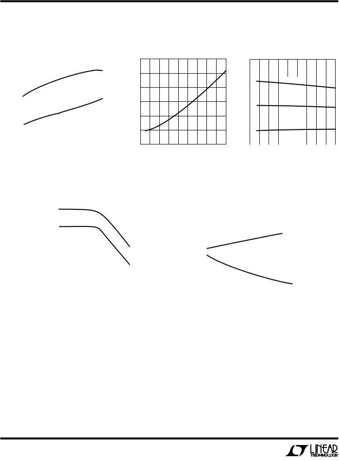
TYPICAL PERFORWAUCE CHARACTERISTICS
VC PIN VOLTAGE (mV)
Shutdown Thresholds
400 |
|
|
|
|
|
|
|
|
|
|
|
|
|
|
|
|
|
|
|
|
|
|
–400 |
|
|
|
|
|
|
|
|
|
|
|
|
|
|
|
|
|
|
|
|
|
|
|
|
||
350 |
|
|
|
|
|
|
|
|
|
|
|
|
|
|
|
|
|
|
|
|
||||
|
CURRENT |
(OUT |
OF V |
C PIN) |
|
|
|
|
|
|
|
|
–350 |
|
||||||||||
|
|
|
|
|
|
|
|
|
|
|
||||||||||||||
300 |
|
|
|
|
|
|
|
|
|
|
|
|
|
|
|
|
|
|
|
|
|
|
–300 |
V |
|
|
|
|
|
|
|
|
|
|
|
|
|
|
|
|
|
|
|
|
|
|
|||
|
|
|
|
|
|
|
|
|
|
|
|
|
|
|
|
|
|
|
|
|
|
|
|
|
|
|
|
|
|
|
|
|
|
|
|
|
|
|
|
|
|
|
|
|
|
|
|
|
C |
250 |
|
|
|
|
|
|
|
|
|
|
|
|
|
|
|
|
|
|
|
|
|
|
–250 |
PIN |
|
|
|
|
|
|
|
|
|
|
|
|
|
|
|
|
|
|
|
|
|
|
|||
200 |
|
|
|
|
|
|
|
|
|
|
|
|
|
|
|
|
|
|
|
|
|
|
–200 |
CURRENT |
150 |
|
|
|
|
|
|
|
|
|
VOLTAGE |
|
|
|
|
|
|
|
|
|
|
–150 |
|
||
|
|
|
|
|
|
|
|
|
|
|
|
|
|
|
|
|
|
|
|
|
|
A)μ( |
||
|
|
|
|
|
|
|
|
|
|
|
|
|
|
|
|
|
|
|
|
|
|
|||
100 |
|
|
|
|
|
|
|
|
|
|
|
|
|
|
|
|
|
|
|
|
|
|
–100 |
|
|
|
|
|
|
|
|
|
|
|
|
|
|
|
|
|
|
|
|
|
|
|
|
||
50 |
|
|
|
|
|
VC VOLTAGE IS REDUCED UNTIL |
|
|
|
–50 |
|
|||||||||||||
|
|
|
|
|
REGULATOR CURRENT DROPS |
|
|
|
|
|
||||||||||||||
|
|
|
|
|
|
|
|
|
|
|||||||||||||||
0 |
|
|
|
|
|
BELOW 300μA |
|
|
|
|
|
|
|
|
|
|
|
0 |
|
|||||
|
|
|
|
|
|
|
|
|
|
|
|
|
|
|
|
|
|
|
|
|
|
|
||
|
–50 |
|
|
0 |
|
|
|
|
|
|
|
100 |
125 |
|
|
|||||||||
–75 |
–25 |
25 |
50 |
75 |
150 |
|
||||||||||||||||||
TEMPERATURE (°C)
1170/1/2 G16
TIME (μs)
Flyback Blanking Time
2.2
2.0
1.8
1.6
1.4
1.2
1.0 |
|
|
|
|
|
100 |
|
|
–75 –50 |
–25 |
0 |
25 |
50 |
75 |
125 |
150 |
JUNCTION TEMPERATURE (°C)
1170/1/2 G17
FLYBACK VOLTAGE (V)
Isolated Mode Flyback Reference
Voltage
23
22 |
|
|
|
|
|
|
|
|
|
|
|
|
|
|
|
|
|
|
|
|
|
|
|
|
|
|
|
|
|
|
|
|
|
|
|
|
|
|
|
|
|
|
|
|
|
|
|
||||||
21 |
|
|
|
|
RFB = 500Ω |
|
|
|
|
|
|
||||||
|
|
|
|
|
|
|
|
|
|
||||||||
20 |
|
|
|
|
|
|
|
|
|
|
|
|
|
|
|
|
|
|
|
|
|
|
|
|
|
|
|
|
|
|
|
|
|
|
|
|
|
|
|
|
|
|
|
|
|
|
|
|
|
|
|
|
|
19 |
|
|
|
|
|
|
|
|
|
|
|
|
|
|
|
|
|
|
|
|
|
|
RFB = |
1k |
|
|
|
|
|
|
|
||||
|
|
|
|
|
|
|
|
|
|
|
|
|
|||||
18 |
|
|
|
|
|
|
|
|
|
|
|
|
|
|
|
|
|
|
|
|
|
|
|
|
|
|
|
|
|
|
|
|
|
|
|
17 |
|
|
|
|
|
|
|
|
|
|
|
|
|
|
|
|
|
|
|
|
|
RFB = 10k |
|
|
|
|
|
|
|||||||
|
|
|
|
|
|
|
|
|
|
|
|||||||
|
|
|
|
|
|
|
|
|
|
|
|
||||||
16 |
|
|
|
|
|
|
|
|
|
|
|
|
|
|
|
|
|
|
|
|
|
|
|
|
|
|
|
|
|
|
|
|
|
|
|
15 |
|
|
|
|
|
|
|
|
|
|
|
|
|
|
|
|
|
|
–50 |
|
0 |
|
|
|
|
|
|
|
|
|
100 |
125 |
|
|
|
–75 |
–25 |
25 |
50 |
|
75 |
150 |
|||||||||||
TEMPERATURE (°C)
1170/1/2 G18
|
Transconductance of Error |
|
|
|
|||||||||||||||||||||||||||||
|
Amplifier |
|
|
|
|
|
|
|
|
|
|
|
|
|
|
|
|
|
|
|
|
||||||||||||
|
7000 |
|
|
|
|
|
|
|
|
|
|
|
|
|
|
|
|
|
|
|
|
|
|
|
|
|
|
|
|
|
|
–30 |
|
|
|
|
|
|
|
|
|
|
|
|
|
|
|
|
|
|
|
|
|
|
|
|
|
|
|
|
|
|
|
|
|
||
|
6000 |
|
|
|
|
|
|
|
|
|
|
|
|
|
|
|
|
|
|
|
|
|
|
|
|
|
|
|
|
|
|
0 |
|
mho) |
|
|
|
|
|
|
|
|
|
|
|
|
|
|
θ |
|
|
|
|
|
|
|
|
|
|
|
|
|
|
|
|||
|
|
|
|
|
|
|
|
|
|
|
|
|
|
|
|
|
|
|
|
|
|
|
|
|
|
|
|
|
|
|
|||
5000 |
|
|
|
|
|
|
|
|
|
|
|
|
|
|
|
|
|
|
|
|
|
|
|
|
|
|
|
|
|
|
30 |
|
|
|
|
|
|
|
|
|
|
|
|
|
|
|
|
|
|
|
|
|
|
|
|
|
|
|
|
|
|
|
|
|
|||
(μ |
|
|
|
|
|
|
|
|
|
|
|
|
|
|
|
|
|
|
|
|
|
|
|
|
|
|
|
|
|
|
|
|
(DEG)PHASE |
TRANSCONDUCTANCE |
4000 |
|
|
|
|
|
|
|
|
|
|
|
|
|
|
|
|
|
|
|
|
|
|
|
|
|
|
|
|
|
|
60 |
|
|
|
|
|
|
|
|
|
|
|
|
|
|
|
|
|
gm |
|
|
|
|
|
|
|
|
|
|
|
|
|
|
|||
|
|
|
|
|
|
|
|
|
|
|
|
|
|
|
|
|
|
|
|
|
|
|
|
|
|
|
|
|
|
||||
|
3000 |
|
|
|
|
|
|
|
|
|
|
|
|
|
|
|
|
|
|
|
|
|
|
|
|
|
|
|
|
|
|
90 |
|
|
|
|
|
|
|
|
|
|
|
|
|
|
|
|
|
|
|
|
|
|
|
|
|
|
|
|
|
|
|
|
|
||
|
2000 |
|
|
|
|
|
|
|
|
|
|
|
|
|
|
|
|
|
|
|
|
|
|
|
|
|
|
|
|
|
|
120 |
|
|
|
|
|
|
|
|
|
|
|
|
|
|
|
|
|
|
|
|
|
|
|
|
|
|
|
|
|
|
|
|
|
||
|
1000 |
|
|
|
|
|
|
|
|
|
|
|
|
|
|
|
|
|
|
|
|
|
|
|
|
|
|
|
|
|
|
150 |
|
|
|
|
|
|
|
|
|
|
|
|
|
|
|
|
|
|
|
|
|
|
|
|
|
|
|
|
|
|
|
|
|
||
|
0 |
|
|
|
|
|
|
|
|
|
|
|
|
|
|
|
|
|
|
|
|
|
|
|
|
|
|
|
|
|
|
180 |
|
|
|
|
|
|
|
|
|
|
|
|
|
|
|
|
|
|
|
|
|
|
|
|
|
|
|
|
|
|
|
|
|
||
–1000 |
|
|
|
|
|
|
|
|
|
|
|
|
|
|
|
|
|
|
|
|
|
|
|
|
|
|
|
|
|
|
210 |
|
|
|
|
|
|
|
|
|
|
|
|
|
|
|
|
|
|
|
|
|
|
|
|
|
|
|
|
|
|
|
|
|
|||
|
1k |
10k |
100k |
|
|
|
|
|
1M |
10M |
|
||||||||||||||||||||||
FREQUENCY (Hz)
1170/1/2 G19
FEEDBACK PIN VOLTAGE (mV)
Normal/Flyback Mode Threshold on Feedback Pin
500 |
|
|
|
|
|
|
|
|
|
|
|
|
|
|
|
|
|
|
–24 |
|
|
|
|
|
|
|
|
|
|
|
|
|
|
|
|
|
|
||
490 |
|
|
|
|
|
|
|
|
|
|
|
|
|
|
|
|
|
|
–22 |
|
|
|
|
|
|
|
|
|
|
|
|
|
|
|
|
|
|
||
480 |
|
|
|
|
|
|
|
|
|
|
|
|
|
|
|
|
|
|
–20 |
|
|
|
|
|
|
|
|
|
|
|
|
|
|
|
|
|
|
||
470 |
|
|
|
|
|
|
|
|
|
|
|
|
|
|
|
|
|
|
–18 |
|
|
|
|
|
|
|
|
|
|
|
|
|
|
|
|
|
|
||
460 |
|
|
|
FEEDBACK PIN VOLTAGE |
|
|
|
|
|
|
–16 |
||||||||
|
|
|
|
(AT THRESHOLD) |
|
|
|
|
|
|
|||||||||
|
|
|
|
|
|
|
|
|
|
||||||||||
|
|
|
|
|
|
|
|
|
|
|
|
||||||||
450 |
|
|
|
|
|
|
|
|
|
|
|
|
|
|
|
|
|
|
–14 |
|
|
|
|
|
|
|
|
|
|
|
|
|
|
|
|
|
|
||
440 |
|
|
|
|
|
|
|
|
|
|
|
|
|
|
|
|
|
|
–12 |
|
|
|
|
|
|
|
|
|
|
|
|
|
|
|
|
|
|
||
430 |
|
|
|
|
FEEDBACK PIN CURRENT |
|
|
|
|
|
–10 |
||||||||
|
|
|
|
|
|
(AT THRESHOLD) |
|
|
|
|
|
|
|||||||
420 |
|
|
|
|
|
|
|
|
|
|
|
|
– 8 |
||||||
|
|
|
|
|
|
|
|
|
|
|
|
|
|
|
|
|
|
||
|
|
|
|
|
|
|
|
|
|
|
|
|
|
|
|
|
|
||
410 |
|
|
|
|
|
|
|
|
|
|
|
|
|
|
|
|
|
|
– 6 |
|
|
|
|
|
|
|
|
|
|
|
|
|
|
|
|
|
|
||
400 |
|
|
|
|
|
|
|
|
|
|
|
|
|
|
|
|
|
|
– 4 |
|
|
|
|
|
|
|
|
|
|
|
|
|
|
|
125 |
|
|||
–50 |
–25 |
0 |
25 |
50 |
75 |
100 |
150 |
||||||||||||
TEMPERATURE (°C)
1170/1/2 G20
A)μ( CURRENT PIN FEEDBACK
6
 Loading...