


Linear Technology LT2078CS8, LT2078, LT2079I, LT2079C, LT2079 Datasheet
...FEATURES
■SO Package with Standard Pinout
■Supply Current per Amplifier: 50μA Max
■Offset Voltage: 70μV Max
■Offset Current: 250pA Max
■Voltage Noise: 0.6μVP-P, 0.1Hz to 10Hz
■Current Noise: 3pAP-P, 0.1Hz to 10Hz
■Offset Voltage Drift: 0.4μV/°C
■Gain Bandwidth Product: 200kHz
■Slew Rate: 0.07V/μs
■Single Supply Operation
Input Voltage Range Includes Ground
Output Swings to Ground while Sinking Current No Pull-Down Resistors Needed
■ Output Sources and Sinks 5mA Load Current
APPLICATIOUS
■Battery or Solar-Powered Systems Portable Instrumentation Remote Sensor Amplifier Satellite Circuitry
■Micropower Sample-and-Hold
■Thermocouple Amplifier
■Micropower Filters
LT2078/LT2079
Micropower, Dual and
Quad, Single Supply,
Precision Op Amps
DESCRIPTIOU
The LT ®2078 is a micropower dual op amp in 8-pin small outline, standard surface mount package, and LT2079 is a micropower quad op amp offered in the standard 14-pin surface mount package. Both devices are optimized for single supply operation at 5V. ±15V specifications are also provided.
Micropowerperformanceofcompetingdevicesisachieved at the expense of seriously degrading precision, noise, speed and output drive specifications. The design effort of the LT2078/LT2079 was concentrated on reducing supply current without sacrificing other parameters. The offset voltage achieved is the lowest on any dual or quad nonchopper stabilized op amp––micropower or otherwise. Offset current, voltage and current noise, slew rate and gain bandwidth product are all two to ten times better than on previous micropower op amps.
Both the LT2078/LT2079 can be operated from a single supply (as low as one lithium cell or two NiCd batteries). The input range goes below ground. The all NPN output stage swings to within a few millivolts of ground while sinking current––no power consuming pull-down resistors are needed. For applications requiring DIP packages refer to the LT1078/LT1079.
, LTC and LT are registered trademarks of Linear Technology Corporation.
TYPICAL APPLICATIOU
Single Battery, Micropower, Gain = 100, Instrumentation Amplifier
|
|
|
|
|
|
|
|
|
10.1k |
|
|
|
|
|
|
1M |
|
|
|
||||||||
|
|
|
|
|
|
|
1M |
2 |
|
|
|
|
|
|
|
|
3V |
|
|
|
|||||||
|
|
|
|
|
|
|
– |
|
|
|
|
|
|
(Li-Ion) |
|
|
|
||||||||||
|
|
|
|
|
|
|
|
|
|
|
|
|
|
|
|
|
|||||||||||
|
|
|
|
|
|
|
|
|
A |
1 |
10.1k |
|
6 |
– |
|
|
|
|
|
8 |
|
|
|
||||
|
|
|
|
|
|
|
|
|
|
|
|
|
|
|
|
|
|
|
|||||||||
|
|
|
|
|
|
|
INVERTING |
3 |
1/2 LT2078 |
|
|
|
|
|
B |
|
|
|
|
|
7 |
|
|
||||
|
|
|
|
|
|
|
|
|
|
|
|
|
|
|
|
|
|
|
|||||||||
|
|
|
|
|
|
|
+ |
|
|
|
|
|
|
|
|
|
|
|
|
|
OUT |
||||||
|
|
|
|
|
|
|
–INPUT |
|
|
NONINVERTING |
5 |
1/2 LT2078 |
|
|
|||||||||||||
|
|
|
|
|
|
|
|
|
|
|
+ |
|
|
|
|
|
|
|
|
|
|
|
|
||||
|
|
|
|
|
|
|
|
|
|
|
|
+INPUT |
|
4 |
|
LT2078/79 • TA01 |
|||||||||||
|
|
|
|
|
|
|
|
|
|
|
|
|
|
|
|||||||||||||
|
|
|
|
|
|
|
|
|
|
|
|
|
|
|
|
|
|
|
|
|
|
|
|
|
|
||
TYPICAL PERFORMANCE |
|
|
|
|
|
|
|
|
|
|
|
|
|
|
|
|
= 85 VP-P 0.1Hz TO 10Hz |
||||||||||
|
|
|
|
|
|
|
|
|
|
|
|
|
|
|
|
||||||||||||
|
|
|
|
|
|
OUTPUT NOISE |
|||||||||||||||||||||
INPUT OFFSET VOLTAGE = 40 V |
|
|
|
|
INPUT RANGE |
= 300 VRMS OVER FULL BANDWIDTH |
|||||||||||||||||||||
INPUT OFFSET CURRENT = 0.2nA |
|
|
|
|
= 0.03V TO 1.8V |
||||||||||||||||||||||
TOTAL POWER DISSIPATION = 240 W |
|
|
|
|
OUTPUT RANGE = 0.03V TO 2.3V |
||||||||||||||||||||||
COMMON MODE REJECTION = 110dB (AMPLIFIER LIMITED) |
|
|
|
|
|
|
|
|
|
|
(0.3mV≤ VIN+ – VIN– ≤ 23mV) |
||||||||||||||||
GAIN BANDWIDTH PRODUCT = 200kHz |
|
|
|
|
OUTPUTS SINK CURRENT—NO PULL-DOWN RESISTORS |
||||||||||||||||||||||
Distribution of Input Offset Voltage
800 VS = 5V, 0V
700 5000 OP AMPS
AMPS |
600 |
|
|
|
|
|
|
|
|
|
|
|
|
|
|
|
|
|
|
|
|
|
|
|
|
||
|
|
|
|
|
|
|
|
|
|
|
|
||
500 |
|
|
|
|
|
|
|
|
|
|
|
|
|
|
|
|
|
|
|
|
|
|
|
|
|
||
OF OP |
|
|
|
|
|
|
|
|
|
|
|
|
|
400 |
|
|
|
|
|
|
|
|
|
|
|
|
|
|
|
|
|
|
|
|
|
|
|
|
|
||
NUMBER |
300 |
|
|
|
|
|
|
|
|
|
|
|
|
|
|
|
|
|
|
|
|
|
|
|
|
|
|
|
200 |
|
|
|
|
|
|
|
|
|
|
|
|
|
|
|
|
|
|
|
|
|
|
|
|
|
|
|
100 |
|
|
|
|
|
|
|
|
|
|
|
|
|
|
|
|
|
|
|
|
|
|
|
|
|
|
|
0 |
|
|
|
|
|
|
|
|
|
|
|
|
|
|
|
|
|
|
|
|
|
|
|
|
|
|
|
|
|
|
|
|
|
|
|
|
|
|
|
|
|
|
–80 |
–40 |
|
40 |
80 |
|
|
|||||
|
–120 |
0 |
120 |
||||||||||
|
|
|
|
INPUT OFFSET VOLTAGE ( V) |
2078/79 • TA02 |
||||||||
1
LT2078/LT2079
ABSOLUTE
WAXIWUW
RATINGSU
Supply Voltage |
...................................................... |
±22V |
Specified Temperature Range |
|
Differential Input Voltage ....................................... |
±30V |
Commercial ............................................. |
0°C to 70°C |
|
Input Voltage ............... |
Equal to Positive Supply Voltage |
Industrial ............................................ |
– 40°C to 85°C |
|
............ |
5V Below Negative Supply Voltage |
Storage Temperature Range ................. |
– 65°C to 150°C |
|
Output Short-Circuit ..........................Duration |
Indefinite |
Lead Temperature (Soldering, 10 sec).................. |
300°C |
|
|
|
|
|
|
|
|
|
|
|
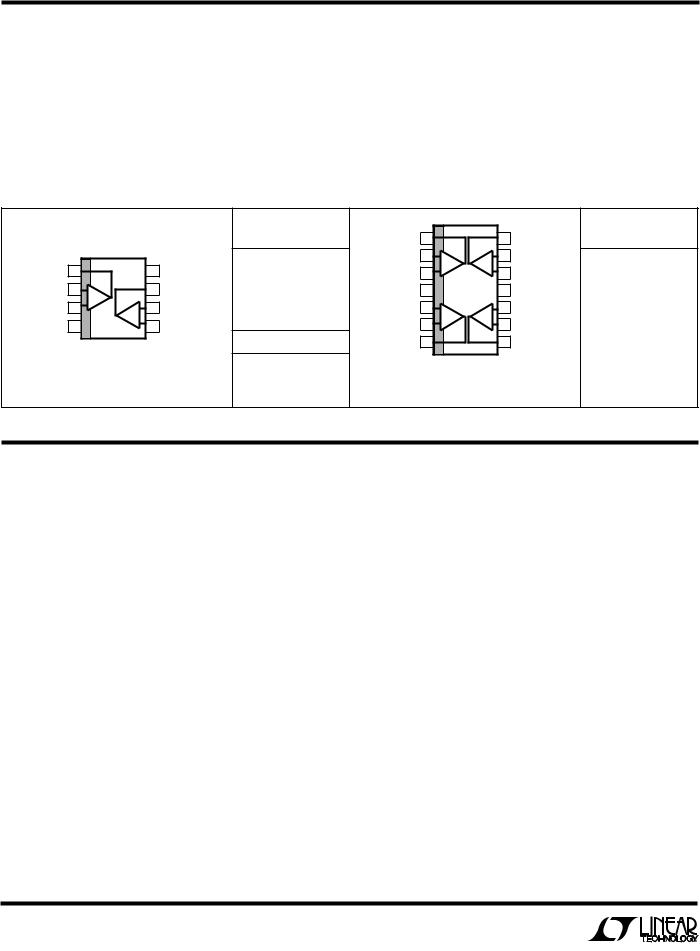
PACKAGE/ORDER IUFORWATIOU
TOP VIEW
OUT A |
1 |
8 |
V+ |
–IN A |
2 |
7 |
OUT B |
+IN A |
3 |
A |
–IN B |
6 |
|||
V– |
4 |
B |
+IN B |
5 |
S8 PACKAGE
8-LEAD PLASTIC SO
TJMAX = 150°C, θJA = 190°C/ W
ORDER PART
NUMBER
LT2078ACS8
LT2078AIS8
LT2078CS8
LT2078IS8
PART MARKING
2078A 2078 2078AI 2078I
TOP VIEW
OUT A |
1 |
14 |
OUT D |
–IN A |
2 |
13 |
–IN D |
|
A |
D |
|
+IN A |
3 |
12 |
+IN D |
V+ |
4 |
11 |
V– |
+IN B |
5 |
10 |
+IN C |
–IN B |
B |
C |
–IN C |
6 |
9 |
||
OUT B |
7 |
8 |
OUT C |
S PACKAGE
14-LEAD PLASTIC SO
TJMAX = 150°C, θJA = 150°C/ W
ORDER PART
NUMBER
LT2079AC
LT2079AI
LT2079C
LT2079I
Consult factory for Military grade parts.
ELECTRICAL CHARACTERISTICS VS = 5V, 0V, VCM = 0.1V, VO = 1.4V, TA = 25°C, unless otherwise noted.
|
|
|
|
LT2078AC/LT2078AI |
LT2078C/LT2078I |
|
|
|
||||
|
|
|
|
LT2079AC/LT2079AI |
LT2079C/LT2079I |
|
|
|
||||
SYMBOL |
PARAMETER |
CONDITIONS (NOTE 1) |
MIN |
TYP |
MAX |
MIN |
TYP |
MAX |
UNITS |
|
||
VOS |
Input Offset Voltage |
LT2078 |
|
30 |
70 |
|
40 |
120 |
|
mV |
||
|
|
|
LT2079 |
|
35 |
110 |
|
40 |
150 |
|
mV |
|
DVOS |
Long Term Input Offset |
|
|
0.4 |
|
|
0.5 |
|
mV/Mo |
|||
DTime |
|
Voltage Stability |
|
|
|
|
|
|
|
|
|
|
|
|
|
|
|
|
|
|
|
|
|
|
|
IOS |
Input Offset Current |
|
|
0.05 |
0.25 |
|
0.05 |
0.35 |
|
nA |
||
IB |
Input Bias Current |
|
|
6 |
8 |
|
6 |
10 |
|
nA |
||
en |
Input Noise Voltage |
0.1Hz to 10Hz (Note 2) |
|
0.6 |
1.2 |
|
0.6 |
|
mVP-P |
|||
|
|
Input Noise Voltage Density |
fO = 10Hz (Note 2) |
|
29 |
45 |
|
29 |
|
nVÖ |
|
|
|
|
|
|
|
Hz |
|||||||
|
|
|
fO = 1000Hz (Note 2) |
|
28 |
37 |
|
28 |
|
nVÖHz |
||
in |
Input Noise Current |
0.1Hz to 10Hz (Note 2) |
|
2.3 |
4.0 |
|
2.3 |
|
pAP-P |
|||
|
|
Input Noise Current Density |
fO = 10Hz (Note 2) |
|
0.06 |
0.10 |
|
0.06 |
|
pAÖ |
|
|
|
|
|
|
|
Hz |
|||||||
|
|
|
fO = 1000Hz |
|
0.02 |
|
|
0.02 |
|
pAÖHz |
||
|
|
|
|
|
|
|
|
|
|
|
|
|
|
|
Input Resistance |
(Note 3) |
|
|
|
|
|
|
MW |
||
|
|
Differential Mode |
|
400 |
800 |
|
300 |
800 |
|
|||
|
|
Common Mode |
|
|
6 |
|
|
6 |
|
GW |
||
|
|
Input Voltage Range |
|
3.5 |
3.8 |
|
3.5 |
3.8 |
|
|
V |
|
|
|
|
|
0 |
– 0.3 |
|
0 |
– 0.3 |
|
|
V |
|
|
|
|
|
|
|
|
|
|
|
|
|
|
CMRR |
Common Mode Rejection Ratio |
VCM = 0V to 3.5V |
95 |
110 |
|
92 |
108 |
|
dB |
|||
PSRR |
Power Supply Rejection Ratio |
VS = 2.3V to 12V |
100 |
114 |
|
98 |
114 |
|
|
dB |
||
|
|
|
|
|
|
|
|
|
|
|
|
|
2

LT2078/LT2079
ELECTRICAL CHARACTERISTICS VS = 5V, 0V, VCM = 0.1V, VO = 1.4V, TA = 25°C, unless otherwise noted.
|
|
|
LT2078AC/LT2078AI |
LT2078C/LT2078I |
|
||||
|
|
|
LT2079AC/LT2079AI |
LT2079C/LT2079I |
|
||||
SYMBOL |
PARAMETER |
CONDITIONS (NOTE 1) |
MIN |
TYP |
MAX |
MIN |
TYP |
MAX |
UNITS |
AVOL |
Large-Signal Voltage Gain |
VO = 0.03V to 4V, No Load |
200 |
1000 |
|
150 |
1000 |
|
V/mV |
|
|
VO = 0.03V to 3.5V, RL = 50k |
150 |
600 |
|
120 |
600 |
|
V/mV |
|
Maximum Output Voltage |
Output Low, No Load |
|
3.5 |
6 |
|
3.5 |
6 |
mV |
|
Swing |
Output Low, 2k to GND |
|
0.55 |
1.0 |
|
0.55 |
1.0 |
mV |
|
|
Output Low, ISINK = 100μA |
|
95 |
130 |
|
95 |
130 |
mV |
|
|
|
|
|
|
|
|
|
|
|
|
Output High, No Load |
4.2 |
4.4 |
|
4.2 |
4.4 |
|
V |
|
|
|
|
||||||
|
|
Output High, 2k to GND |
3.5 |
3.9 |
|
3.5 |
3.9 |
|
V |
|
|
|
|
|
|
|
|
|
|
SR |
Slew Rate |
AV = 1, VS = ±2.5V |
0.04 |
0.07 |
|
0.04 |
0.07 |
|
V/μs |
GBW |
Gain Bandwidth Product |
fO ≤ 20kHz |
|
200 |
|
|
200 |
|
kHz |
IS |
Supply Current per Amplifier |
|
|
38 |
50 |
|
39 |
55 |
μA |
|
Channel Separation |
VIN = 3V, RL = 10k, f ≤ 10Hz |
|
110 |
|
|
110 |
|
dB |
|
Minimum Supply Voltage |
(Note 4) |
|
2.2 |
2.3 |
|
2.2 |
2.3 |
V |
|
|
|
|
|
|
|
|
|
|
VS = 5V, 0V, VCM = 0.1V, VO = 1.4V, – 40°C ≤ TA ≤ 85°C for I grades, unless otherwise noted.
|
|
|
|
|
|
LT2078AI/LT2079AI |
LT2078I/LT2079I |
|
||||
|
SYMBOL |
PARAMETER |
CONDITIONS |
|
MIN |
TYP |
MAX |
MIN |
TYP |
MAX |
UNITS |
|
|
|
|
|
|
|
|
|
|
|
|
|
|
|
VOS |
Input Offset Voltage |
LT2078 |
● |
|
70 |
250 |
|
95 |
370 |
μV |
|
|
|
|
|
LT2079 |
● |
|
80 |
280 |
|
100 |
400 |
μV |
|
VOS |
Input Offset Voltage Drift |
LT2078 |
● |
|
0.4 |
1.8 |
|
0.5 |
2.5 |
μV/°C |
|
|
T |
|
(Note 5) |
LT2079 |
● |
|
0.6 |
3.0 |
|
0.6 |
3.5 |
μV/°C |
|
|
|
|
|
|
|
|
|
|
|
|
|
|
IOS |
Input Offset Current |
|
● |
|
0.07 |
0.70 |
|
0.1 |
1.0 |
nA |
|
|
IB |
Input Bias Current |
|
● |
|
7 |
10 |
|
7 |
12 |
nA |
|
|
CMRR |
Common Mode Rejection Ratio |
VCM = 0.05V to 3.2V |
● |
90 |
106 |
|
86 |
104 |
|
dB |
|
|
PSRR |
Power Supply Rejection Ratio |
VS = 3.1V to 12V |
● |
96 |
110 |
|
92 |
110 |
|
dB |
|
|
AVOL |
Large-Signal Voltage Gain |
VO = 0.05V to 4V, No Load |
● |
110 |
600 |
|
80 |
600 |
|
V/mV |
|
|
|
|
|
VO = 0.05V to 3.5V, RL = 50k |
● |
80 |
400 |
|
60 |
400 |
|
V/mV |
|
|
|
Maximum Output Voltage |
Output Low, No Load |
● |
|
4.5 |
8 |
|
4.5 |
8 |
mV |
|
|
|
Swing |
Output Low, ISINK = 100μA |
● |
|
125 |
170 |
|
125 |
170 |
mV |
|
|
|
|
Output High, No Load |
● |
3.9 |
4.2 |
|
3.9 |
4.2 |
|
V |
|
|
|
|
|
|
|||||||
|
|
|
|
Output High, 2k to GND |
● |
3.0 |
3.7 |
|
3.0 |
3.7 |
|
V |
|
|
|
|
|
|
|
|
|
|
|
|
|
|
IS |
Supply Current per Amplifier |
|
● |
|
43 |
60 |
|
45 |
70 |
μA |
|
VS = 5V, 0V, VCM = 0.1V, VO = 1.4V, 0°C ≤ TA ≤ 70°C, unless otherwise noted (Note 6).
|
|
|
|
|
|
|
|
|
|
|
|
|
|
|
|
|
LT2078AC/LT2079AC |
LT2078C/LT2079C |
|
||||
SYMBOL |
PARAMETER |
CONDITIONS |
|
MIN |
TYP |
MAX |
MIN |
TYP |
MAX |
UNITS |
|||||||||||||
|
|
|
|
|
|
|
|
|
|
|
|||||||||||||
VOS |
Input Offset Voltage |
LT2078 |
● |
|
50 |
150 |
|
60 |
240 |
μV |
|||||||||||||
|
|
|
|
|
|
|
|
|
|
|
|
|
|
|
LT2079 |
● |
|
60 |
180 |
|
70 |
270 |
μV |
|
|
|
|
|
|
|
|
|
|
|
|||||||||||||
VOS |
Input Offset Voltage Drift |
LT2078 |
● |
|
0.4 |
1.8 |
|
0.5 |
2.5 |
μV/°C |
|||||||||||||
T |
(Note 5) |
LT2079 |
● |
|
0.5 |
3.0 |
|
0.6 |
3.5 |
μV/°C |
|||||||||||||
|
|
|
|
|
|
|
|
|
|
|
|||||||||||||
IOS |
Input Offset Current |
|
● |
|
0.06 |
0.35 |
|
0.06 |
0.50 |
nA |
|||||||||||||
IB |
Input Bias Current |
|
● |
|
6 |
9 |
|
6 |
11 |
nA |
|||||||||||||
CMRR |
Common Mode Rejection Ratio |
VCM = 0V to 3.4V |
● |
92 |
108 |
|
88 |
106 |
|
dB |
|||||||||||||
PSRR |
Power Supply Rejection Ratio |
VS = 2.6V to 12V |
● |
98 |
112 |
|
95 |
112 |
|
dB |
|||||||||||||
|
|
|
|
|
|
|
|
|
|
|
|
|
|
|
|
|
|
|
|
|
|
|
|
|
|
|
|
|
|
|
|
|
|
|
|
|
|
|
|
|
|
|
|
|
|
|
|
|
|
|
|
|
|
|
|
|
|
|
|
|
|
|
|
|
|
|
|
|
|
|
3 |
|
|
|
|
|
|
|
|
|
|
|
|
|
|
|
|
|
|
|
|
|
|
|
|
|
|
|
|
|
|
|
|
|
|
|
|
|
|
|
|
|
|
|
|
|
|
|
|

LT2078/LT2079
ELECTRICAL CHARACTERISTICS VS = 5V, 0V, VCM = 0.1V, VO = 1.4V, 0°C ≤ TA ≤ 70°C, unless otherwise noted.
|
|
|
|
|
LT2078AC/LT2079AC |
LT2078C/LT2079C |
|
||||
|
SYMBOL |
PARAMETER |
CONDITIONS |
|
MIN |
TYP |
MAX |
MIN |
TYP |
MAX |
UNITS |
|
|
|
|
|
|
|
|
|
|
|
|
|
AVOL |
Large-Signal Voltage Gain |
VO = 0.05V to 4V, No Load |
● |
150 |
750 |
|
110 |
750 |
|
V/mV |
|
|
|
VO = 0.05V to 3.5V, RL = 50k |
● |
110 |
500 |
|
80 |
500 |
|
V/mV |
|
|
Maximum Output Voltage |
Output Low, No Load |
● |
|
4.0 |
7 |
|
4.0 |
7 |
mV |
|
|
Swing |
Output Low, ISINK = 100μA |
● |
|
105 |
150 |
|
105 |
150 |
mV |
|
|
|
|
|
|
|
|
|
|
|
|
|
|
|
Output High, No Load |
● |
4.1 |
4.3 |
|
4.1 |
4.3 |
|
V |
|
|
|
|
|
|||||||
|
|
|
Output High, 2k to GND |
● |
3.3 |
3.8 |
|
3.3 |
3.8 |
|
V |
|
|
|
|
|
|
|
|
|
|
|
|
|
IS |
Supply Current per Amplifier |
|
● |
|
40 |
55 |
|
42 |
63 |
μA |
VS = ±15V, TA = 25°C, unless otherwise noted.
|
|
|
LT2078AC/LT2078AI |
LT2078C/LT2078I |
|
||||
|
|
|
LT2079AC/LT2079AI |
LT2079C/LT2079I |
|
||||
SYMBOL |
PARAMETER |
CONDITIONS |
MIN |
TYP |
MAX |
MIN |
TYP |
MAX |
UNITS |
VOS |
Input Offset Voltage |
LT2078 |
|
50 |
250 |
|
70 |
350 |
μV |
|
|
LT2079 |
|
60 |
350 |
|
80 |
450 |
μV |
IOS |
Input Offset Current |
|
|
0.05 |
0.25 |
|
0.05 |
0.35 |
nA |
IB |
Input Bias Current |
|
|
6 |
8 |
|
6 |
10 |
nA |
|
Input Voltage Range |
|
13.5 |
13.8 |
|
13.5 |
13.8 |
|
V |
|
|
|
–15.0 |
–15.3 |
|
–15.0 |
–15.3 |
|
V |
|
|
|
|
|
|
|
|
|
|
CMRR |
Common Mode Rejection Ratio |
VCM = 13.5V, –15V |
98 |
114 |
|
95 |
114 |
|
dB |
PSRR |
Power Supply Rejection Ratio |
VS = 5V, 0V to ±18V |
100 |
114 |
|
98 |
114 |
|
dB |
AVOL |
Large-Signal Voltage Gain |
VO = ±10V, RL = 50k |
1000 |
5000 |
|
1000 |
5000 |
|
V/mV |
|
|
VO = ±10V, RL = 2k |
400 |
1100 |
|
300 |
1100 |
|
V/mV |
VOUT |
Maximum Output Voltage |
RL = 50k |
±13.0 |
±14.0 |
|
±13.0 |
±14.0 |
|
V |
|
Swing |
RL = 2k |
±11.0 |
±13.2 |
|
±11.0 |
±13.2 |
|
V |
SR |
Slew Rate |
|
0.06 |
0.10 |
|
0.06 |
0.10 |
|
V/μs |
|
|
|
|
|
|
|
|
|
|
IS |
Supply Current per Amplifier |
|
|
46 |
65 |
|
47 |
75 |
μA |
VS = ±15V, – 40°C ≤ TA ≤ 85°C for I grades, unless otherwise noted.
|
|
|
|
|
LT2078AI/LT2079AI |
LT2078I/LT2079I |
|
||||
SYMBOL |
PARAMETER |
CONDITIONS |
|
MIN |
TYP |
MAX |
MIN |
TYP |
MAX |
UNITS |
|
VOS |
Input Offset Voltage |
LT2078 |
● |
|
90 |
430 |
|
120 |
600 |
μV |
|
|
|
|
LT2079 |
● |
|
100 |
500 |
|
130 |
700 |
μV |
|
|
|
|
|
|
|
|
|
|
|
|
VOS |
Input Offset Voltage Drift |
LT2078 |
● |
|
0.5 |
1.8 |
|
0.6 |
2.5 |
μV/°C |
|
T |
|
(Note 5) |
LT2079 |
● |
|
0.6 |
3.0 |
|
0.7 |
3.8 |
μV/°C |
|
|
|
|
|
|
|
|
|
|
|
|
IOS |
Input Offset Current |
|
● |
|
0.07 |
0.70 |
|
0.1 |
1.0 |
nA |
|
IB |
Input Bias Current |
|
● |
|
7 |
10 |
|
7 |
12 |
nA |
|
AVOL |
Large-Signal Voltage Gain |
VO = ±10V, RL = 5k |
● |
200 |
700 |
|
150 |
700 |
|
V/mV |
|
CMRR |
Common Mode Rejection Ratio |
VCM = 13V, –14.9V |
● |
92 |
110 |
|
88 |
110 |
|
dB |
|
PSRR |
Power Supply Rejection Ratio |
VS = 5V, 0V to ±18V |
● |
96 |
110 |
|
92 |
110 |
|
dB |
|
|
|
Maximum Output Voltage Swing |
RL = 5k |
● |
±11.0 |
±13.5 |
|
±11.0 |
±13.5 |
|
V |
IS |
Supply Current per Amplifier |
|
● |
|
52 |
80 |
|
54 |
95 |
μA |
|
4

LT2078/LT2079
ELECTRICAL CHARACTERISTICS |
VS = ±15V, 0°C ≤ TA ≤ 70°C, unless otherwise noted (Note 6). |
|
|||||||||
|
|
|
|
|
LT2078AC/LT2079AC |
LT2078C/LT2079C |
|
||||
SYMBOL |
PARAMETER |
CONDITIONS |
|
|
MIN |
TYP |
MAX |
MIN |
TYP |
MAX |
UNITS |
VOS |
Input Offset Voltage |
LT2078 |
|
● |
|
70 |
330 |
|
90 |
460 |
μV |
|
|
LT2079 |
|
● |
|
80 |
410 |
|
100 |
540 |
μV |
VOS |
Input Offset Voltage Drift |
LT2078 |
|
● |
|
0.5 |
1.8 |
|
0.6 |
2.5 |
μV/°C |
T |
(Note 5) |
LT2079 |
|
● |
|
0.6 |
3.0 |
|
0.7 |
3.8 |
μV/°C |
|
|
|
|
|
|
|
|
|
|
|
|
IOS |
Input Offset Current |
|
|
● |
|
0.06 |
0.35 |
|
0.06 |
0.50 |
nA |
IB |
Input Bias Current |
|
|
● |
|
6 |
9 |
|
6 |
11 |
nA |
AVOL |
Large-Signal Voltage Gain |
VO = ±10V, RL = 5k |
|
● |
300 |
1200 |
|
250 |
1200 |
|
V/mV |
CMRR |
Common Mode Rejection Ratio |
VCM = 13V, –15V |
|
● |
95 |
112 |
|
92 |
112 |
|
dB |
PSRR |
Power Supply Rejection Ratio |
VS = 5V, 0V to ±18V |
|
● |
98 |
112 |
|
95 |
112 |
|
dB |
|
Maximum Output Voltage Swing |
RL = 5k |
|
● |
±11.0 |
±13.6 |
|
±11.0 |
±13.6 |
|
V |
IS |
Supply Current per Amplifier |
|
|
● |
|
49 |
73 |
|
50 |
85 |
μA |
The ● denotes specifications which apply over the full operating temperature range.
Note 1: Typical parameters are defined as the 60% yield of parameter distributions of individual amplifiers, i.e., out of 100 LT2079s (or 100 LT2078s) typically 240 op amps (or 120) will be better than the indicated specification.
Note 2: This parameter is tested on a sample basis only. All noise parameters are tested with VS = ±2.5V, VO = 0V.
Note 3: This parameter is guaranteed by design and is not tested. Note 4: Power supply rejection ratio is measured at the minimum supply
voltage. The op amps actually work at 1.8V supply but with a typical offset skew of –300μV.
Note 5: This parameter is not 100% tested.
Note 6: The LT2078C/LT2079C are designed, characterized and expected to meet the industrial temperature limits, but are not tested at – 40°C and 85°C. I-grade parts are guaranteed.
TYPICAL PERFORWAUCE CHARACTERISTICS
PERCENT OF UNITS (%)
Distribution of Offset Voltage
Drift with Temperature
25
VS = 5V, 0V
VCM = 0.1V
2080 LT2078'S
25 LT2079'S
= 260 OP AMPS
15
10
5
0
–2 |
–1 |
0 |
1 |
2 |
OFFSET VOLTAGE DRIFT WITH TEMPERATURE ( V/°C)
LT2078/79 • TPC01
BIAS CURRENT (nA) OFFSET CURRENT (pA)
Input Bias and Offset Currents vs |
Input Bias Current vs |
Temperature |
Common Mode Voltage |
100 |
|
|
|
|
|
|
|
0 |
|
|
|
|
|
VS = 5V, 0V TO ±15V |
|
|
|
|
|
VS = 5V, 0V |
|
|
|
|
|||
50 |
|
|
IOS |
|
|
|
(nA) |
–2 |
|
TA = 125°C |
|
|
|
|
|
|
|
|
|
|
|
|
|
|
|||
|
|
|
|
|
|
|
|
|
|
|
TA = –55°C |
|
|
0 |
|
|
|
|
|
|
CURRENT |
–4 |
|
|
|
|
|
|
|
|
|
|
|
–6 |
|
|
TA = 25°C |
|
|||
|
|
|
|
|
|
|
|
|
|
|
|
|
|
–5 |
|
|
|
|
|
|
BIAS |
|
|
|
|
|
|
|
|
|
|
|
|
|
|
|
|
|
|
|
|
|
|
|
IB |
|
|
|
INPUT |
–8 |
|
|
|
|
|
|
|
|
|
|
|
|
|
|
|
|
|
||
|
|
|
|
|
|
|
|
|
|
|
|
|
|
–6 |
|
|
|
|
|
|
|
–10 |
|
|
|
|
|
|
|
|
|
|
|
|
|
|
|
|
|
|
|
–7 |
|
|
25 |
50 |
|
|
125 |
–12 |
|
|
|
|
|
–50 |
–25 |
0 |
75 |
100 |
–1 |
0 |
1 |
2 |
3 |
4 |
|||
|
|
TEMPERATURE (°C) |
|
|
|
COMMON MODE VOLTAGE (V) |
|
||||||
|
|
|
|
|
|
LT2078/79 • TPC02 |
|
|
|
|
LT2078/79 • TPC03 |
||
5
 Loading...