


LTC1174CN8-5
Linear Technology LTC1174CN8-5, LTC1174CN8-3.3, LTC1174CN8, LTC1174IS8, LTC1174HVCS8-3.3 Datasheet
...
FEATURES
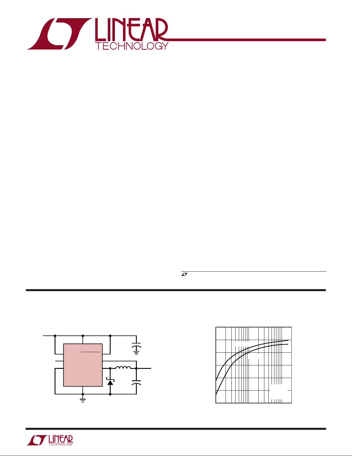
LOAD CURRENT (mA)
1
EFFICIENCY (%)
100
95
90
85
80
75
70
10 100
1174 TA02
200
VIN = 6V
V
IN
= 9V
L = 100µH
V
OUT
= 5V
I
PGM
= 0V
■
High Efficiency: Up to 94%
■
Peak Inductor Current Independent of
Inductor Value
■
Short-Circuit Protection
■
Optimized for 5V to –5V Applications
■
Wide VIN Range: 4V to 18.5V
■
Low Dropout Operation
■
Low-Battery Detector
■
Pin Selectable Current Limit
■
Internal 0.9Ω Power Switch: VIN = 9V
■
Only Four External Components Required
■
130µA Standby Current
■
Active Low Micropower Shutdown
U
APPLICATIO S
■
Distributed Power Systems
■
Step-Down Converters
■
Inverting Converters
■
Memory Backup Supply
■
Portable Instruments
■
Battery-Powered Equipment
LTC1174
LTC1174-3.3/LTC1174-5
High Efficiency
Step-Down and Inverting
DC/DC Converter
U
DESCRIPTIO
The LTC®1174 is a simple current mode DC/DC converter
ideally suited for 9V to 5V, 5V to 3.3V or 5V to –5V
operation. With an internal 0.9Ω switch (at a supply
voltage of 9V), the LTC1174 requires only four external
components to construct a complete high efficiency
DC/DC converter.
Under a no load condition the LTC1174 draws only 130µA.
In shutdown, it draws a mere 1µA making this converter
ideal for current sensitive applications. In dropout, the
internal P-channel MOSFET switch is turned on continuously allowing the user to maximize the life of the battery
source.
The maximum inductor current of the LTC1174 family is
pin selectable to either 340mA or 600mA, optimizing
efficiency for a wide range of applications. Operation up to
200kHz permits the use of small surface mount inductors
and capacitors.
For applications requiring higher output current or ultrahigh efficiency, see the LTC1148 data sheet.
and LTC are registered trademarks and LT is a trademark of Linear Technology Corporation.
TYPICAL APPLICATIO
High Efficiency Step-Down Converter
V
IN
9V
3
2
7
(3) AVX TPSD156K025
*
AVX TPSD107K010
**
†
COILTRONICS CTX100-4
LB
LB
I
PGM
V
SHUTDOWN
IN
OUT
LTC1174-5
GND
6
IN
4
8
1
V
OUT
5
SW
U
100µH
1N5818
LTC1174-5 Efficiency
15µF*
+
25V
×3
†
+
5V
175mA
100µF**
10V
1174 TA01
1
LTC1174
LTC1174-3.3/LTC1174-5
WWWU
ABSOLUTE AXI U RATI GS
(Note 1)
(Voltage Referred to GND Pin)
Input Supply Voltage (Pin 6)
LTC1174........................................... –0.3V to 13.5V
LTC1174HV ...................................... –0.3V to 18.5V
Switch Current (Pin 5) .............................................. 1A
Switch Voltage (Pin 5)
LTC1174................................................. VIN – 13.5V
LTC1174HV ............................................ VIN – 18.5V
UU
W
PACKAGE/ORDER I FOR ATIO
ORDER PART
NUMBER
LTC1174CN8
TOP VIEW
(VFB*)
V
OUT
1
LB
2
OUT
LB
3
IN
GND
4
N8 PACKAGE
8-LEAD PDIP
* ADJUSTABLE OUTPUT VERSION
T
= 125°C, θJA = 110°C/W
JMAX
SHUTDOWN
8
I
7
PGM
V
6
IN
SW
5
LTC1174CN8-3.3
LTC1174CN8-5
LTC1174IN8
LTC1174HVCN8
LTC1174HVCN8-3.3
LTC1174HVCN8-5
Operating Temperature Range
LTC1174CX ............................................ 0°C to 70°C
LTC1174IX ........................................ –40°C to 85°C
Junction Temperature (Note 2)............................ 125°C
Storage Temperature Range ................ –65°C to 150°C
Lead Temperature (Soldering, 10 sec)................. 300°C
ORDER PART
NUMBER
LTC1174CS8
TOP VIEW
V
(VFB*)
OUT
1
LB
2
OUT
LB
3
IN
GND
4
S8 PACKAGE
8-LEAD PLASTIC SO
* ADJUSTABLE OUTPUT VERSION
T
= 125°C, θJA = 150°C/W
JMAX
SHUTDOWN
8
I
7
PGM
V
6
IN
SW
5
LTC1174CS8-3.3
LTC1174CS8-5
LTC1174IS8
LTC1174HVCS8
LTC1174HVCS8-3.3
LTC1174HVCS8-5
LTC1174HVIS8
S8 PART MARKING
1174
117433
117450
1174I
1174HV
1174H3
1174H5
1174HI
Consult factor for Military grade parts.
ELECTRICAL CHARACTERISTICS
temperature range, otherwise specifications are at TA = 25°C. VIN = 9V, V
SYMBOL PARAMETER CONDITIONS MIN TYP MAX UNITS
I
V
V
∆V
FB
FB
OUT
Feedback Current LTC1174/LTC1174HV 1 µA
Feedback Voltage LTC1174/LTC1174HV ● 1.20 1.25 1.30 V
Regulated Output Voltage LTC1174-3.3/LTC1174HV-3.3 ● 3.14 3.30 3.46 V
LTC1174-5/LTC1174V-5
Output Voltage Line Regulation VIN = 6V to 12V, I
OUT
Output Voltage Load Regulation LTC1174-3.3 (Note 3)
20mA < I
20mA < I
LTC1174-5 (Note 3)
20mA < I
20mA < I
The ● denotes specifications which apply over the full operating
LOAD
< 175mA, I
LOAD
< 400mA, I
LOAD
< 175mA, I
LOAD
< 400mA, I
LOAD
= 100mA, I
PGM
PGM
PGM
PGM
SHUTDOWN
PGM
= 0V –5 –70 mV
= V
= 0V –5 –70 mV
= V
= VIN, I
= VIN (Note 3) 10 70 mV
IN
IN
= 0V, unless otherwise noted.
PGM
● 4.75 5.00 5.25 V
–45 –70 mV
–50 –70 mV
2
LTC1174
LTC1174-3.3/LTC1174-5
ELECTRICAL CHARACTERISTICS
temperature range, otherwise specifications are at TA = 25°C. VIN = 9V, V
The ● denotes specifications which apply over the full operating
SHUTDOWN
= VIN, I
= 0V, unless otherwise noted.
PGM
SYMBOL PARAMETER CONDITIONS MIN TYP MAX UNITS
I
Q
Input DC Supply Current (Note 4) Active Mode
LTC1174: 4V < V
LTC1174HV: 4V < VIN < 16V, I
< 12V, I
IN
= 0V 450 600 µA
PGM
= 0V 450 600 µA
PGM
Sleep Mode
LTC1174: 4V < V
< 12V 130 180 µA
IN
LTC1174HV: 4V < VIN < 16V 130 180 µA
SHUTDOWN (Note 4)
= 0V, 4V < VIN < 12V 1 10 µA
SHUTDOWN
= 0V, 4V < VIN < 16V 2 25 µA
= 0.4V 1.0 1.2 1.5 mA
= 0.4V 0.6 0.8 1.5 mA
LBOUT
= 0V ● 0.54 0.60 0.78 A
OUT
= 0V ● 0.27 0.34 0.50 A
V
LBTRIP
I
LBIN
I
LBOUT
V
HYST
I
PEAK
R
ON
LTC1174: V
SHUTDOWN
LTC1174HV: V
Low-Battery Trip Point 1.25 1.4 V
Current into Pin 3 0.5 µA
Current Sunk by Pin 2 LTC1174: V
LBOUT
LTC1174HV: V
Comparator Hysteresis LTC1174/LTC1174HV 7.5 15 30 mV
Current Limit I
PGM
I
PGM
= VIN, V
= 0V, V
OUT
ON Resistance of Switch LTC1174 ● 0.75 1.30 Ω
LTC1174HV ● 0.90 1.55 Ω
t
V
V
I
I
OFF
IH
IL
IH
IL
Switch Off-Time (Note 6) V
at Regulated Value 3 4 5 µs
OUT
SHUTDOWN Pin High Minimum Voltage at Pin 8 for Device to Be Active 1.2 V
SHUTDOWN Pin Low Maximum Voltage at Pin 8 for Device to Be in Shutdown 0.75 V
SHUTDOWN Pin Input Current LTC1174: V
LTC1174HV: V
SHUTDOWN Pin Input Current 0 ≤ V
SHUTDOWN
SHUTDOWN
= 12V 0.5 µA
SHUTDOWN
= 16V 2.0 µA
≤ 0.8V 0.5 µA
The ● denotes specifications which apply over the full operating temperature range,
otherwise specifications are at –40°C ≤ TA ≤ 85°C. LTC1174I and LTC1174HVI Only.
SYMBOL PARAMETER CONDITIONS MIN TYP MAX UNITS
V
FB
I
LBOUT
I
PEAK
t
OFF
R
ON
Note 1: Absolute Maximum Ratings are those values beyond which the life
of a device may be impaired.
Note 2: T
dissipation P
Feedback Voltage LTC1174I/LTC1174HVI ● 1.18 1.25 1.31 V
Current Sunk by Pin 2 V
Current Limit I
Switch Off-Time (Note 6) V
= 0.4V (LTC1174I) ● 0.75 1.2 2.0 mA
LBOUT
V
= 0.4V (LTC1174HVI) ● 0.50 0.8 1.6 mA
LBOUT
= VIN, V
PGM
I
= 0V, V
PGM
I
= VIN, V
PGM
I
= 0V, V
PGM
at Regulated Value (LTC1174I) ● 2.0 4 6.0 µs
OUT
V
at Regulated Value (LTC1174HVI) ● 1.8 4 6.2 µs
OUT
= 0V (LTC1174I) ● 0.54 0.60 0.78 A
OUT
= 0V (LTC1174I) 0.34 A
OUT
= 0V (LTC1174HVI) ● 0.5 0.60 0.8 A
OUT
= 0V (LTC1174HVI) 0.34 A
OUT
Switch On Resistance LTC1174I/LTC1174HVI ● 0.9 1.7 Ω
Note 3: Guaranteed by design.
Note 4: Dynamic supply current is higher due to the gate charge being
is calculated from the ambient temperature TA and power
J
according to the following formulas:
D
LTC1174CN8, LTC1174CN8-3.3, LTC1174CN8-5:
= TA + (PD × 110°C/W)
T
J
delivered at the switching frequency.
Note 5: Current into Pin 6 only, measured without electrolytic input
capacitor.
Note 6: The off-time is wafer-sort trimmed.
LTC1174CS8, LTC1174CS8-3.3, LTC1174CS8-5:
= TA + (PD × 150°C/W)
T
J
3
LTC1174
LTC1174-3.3/LTC1174-5
UW
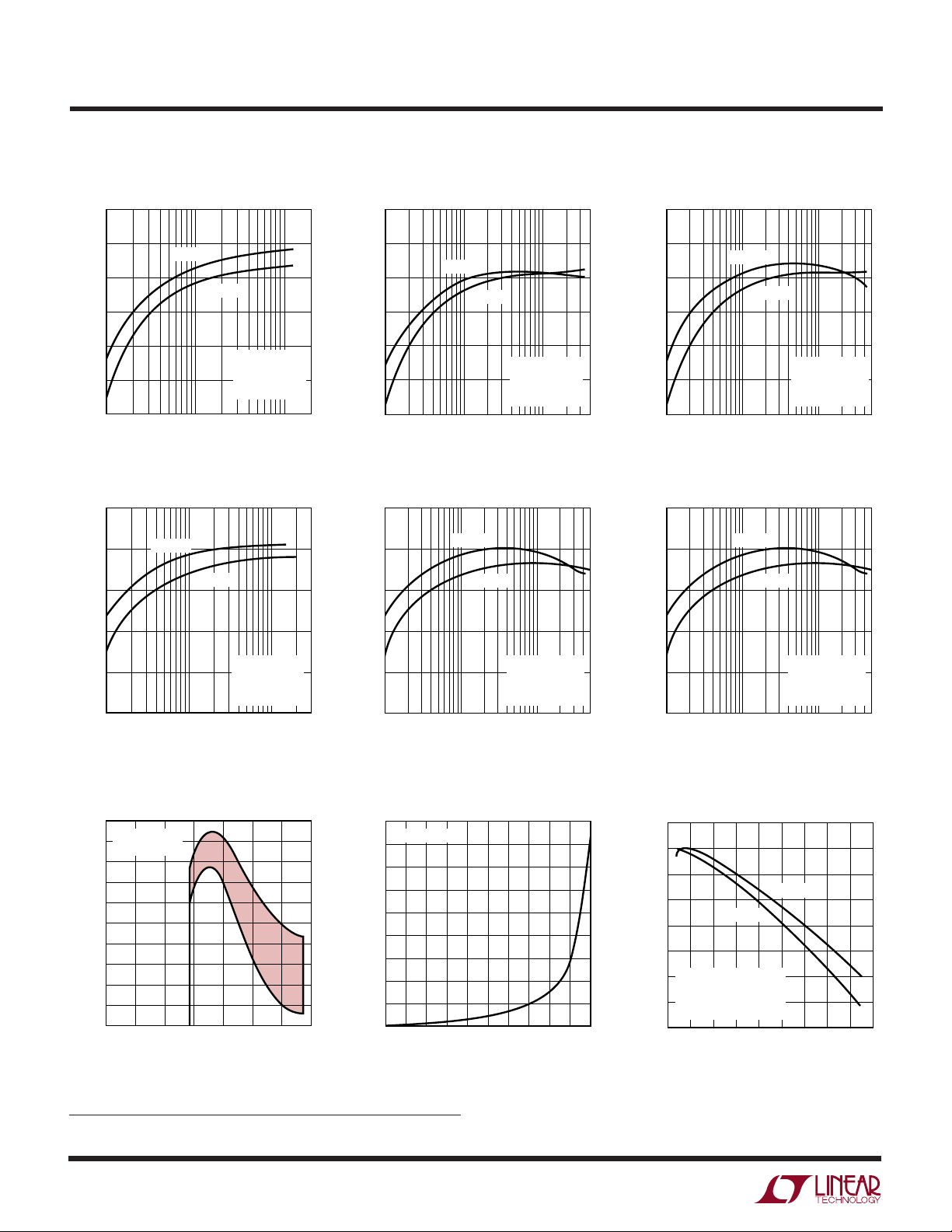
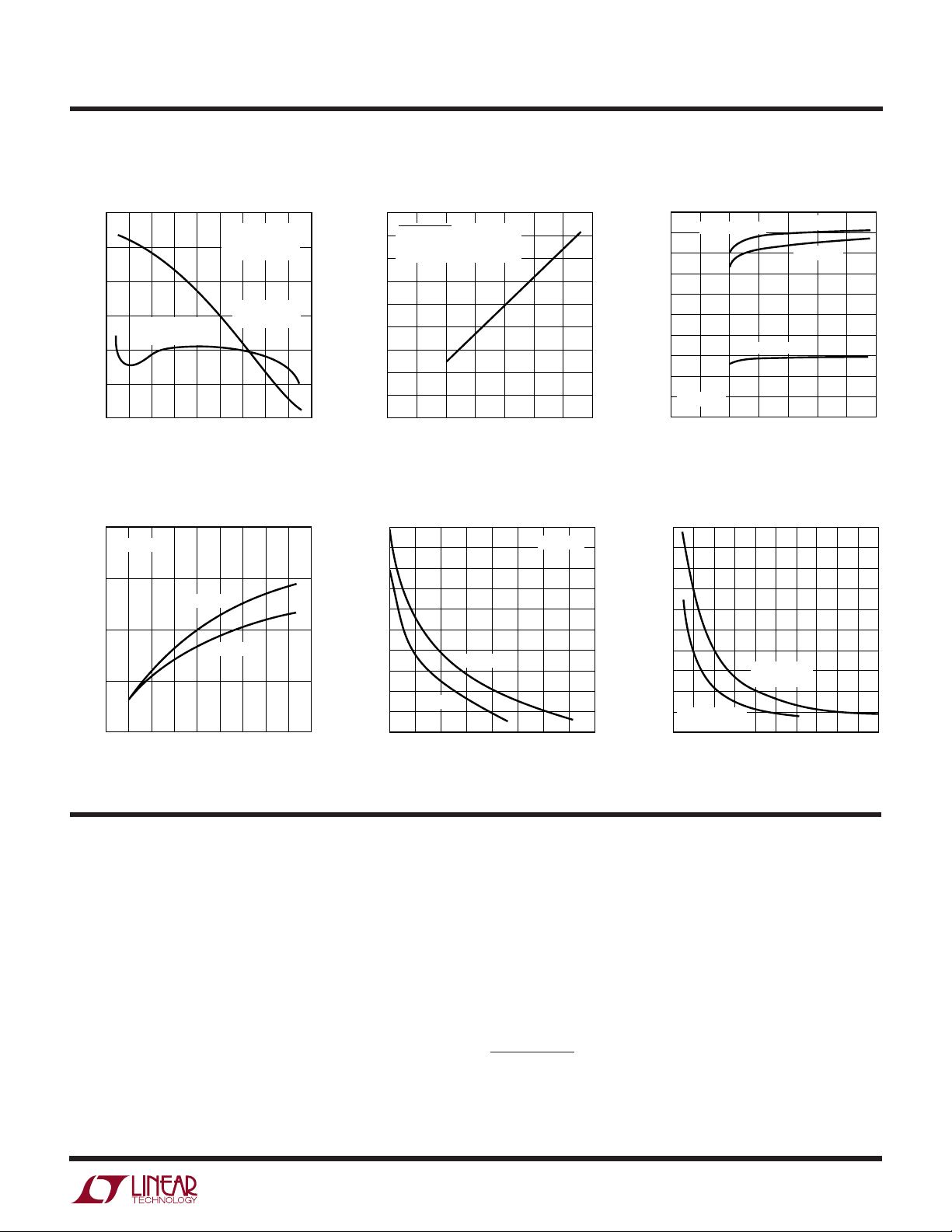
TYPICAL PERFOR A CE CHARACTERISTICS
Efficiency vs Load Current Efficiency vs Load Current Efficiency vs Load Current
100
100
100
95
90
85
EFFICIENCY (%)
80
75
70
1
100
90
80
70
EFFICIENCY (%)
60
50
1
VIN = 6V
= 9V
V
IN
10 100
LOAD CURRENT (mA)
VIN = 5V
VIN = 9V
10 100
LOAD CURRENT (mA)
L = 50µH
V
= 5V
OUT
= 0V
I
PGM
COIL = CTX50-4
1174 G01
L = 50µH
V
= 3.3V
OUT
= 0V
I
PGM
COIL = CTX50-4
1174 G04
200
300
95
90
85
EFFICIENCY (%)
80
75
70
1
100
90
80
70
EFFICIENCY (%)
60
50
1
VIN = 6V
VIN = 9V
L = 50µH
V
OUT
I
PGM
COIL = CTX50-4
10 100
LOAD CURRENT (mA)
VIN = 5V
VIN = 9V
L = 100µH
V
OUT
I
PGM
COIL = CTX100-4
10 100
LOAD CURRENT (mA)
= 5V
= V
= 3.3V
= V
IN
IN
1174 G02
1174 G06
400
500
95
90
85
EFFICIENCY (%)
80
75
70
1
Efficiency vs Load CurrentEfficiency vs Load Current Efficiency vs Load Current
100
90
80
70
EFFICIENCY (%)
60
50
1
VIN = 6V
VIN = 9V
L = 100µH
V
OUT
I
PGM
COIL = CTX100-4
10 100
LOAD CURRENT (mA)
VIN = 5V
VIN = 9V
L = 100µH
V
OUT
I
PGM
COIL = CTX100-4
10 100
LOAD CURRENT (mA)
= 5V
= V
= 3.3V
= V
IN
IN
500
1174 G03
500
1174 G06
Line Regulation
6
I
= 100mA
LOAD
4
= 0V
I
PGM
2
0
–2
(mV)
–4
OUT
–6
∆V
–8
–10
–12
–14
0
Kool Mµ is a registered trademark of Magnetics, Inc.
4
2
INPUT VOLTAGE (V)
8
6
10
12
4
1174 G07
Switch Leakage Current
vs Temperature Efficiency vs Input Voltage
180
VIN = 13.5V
160
140
120
100
80
60
LEAKAGE CURRENT (nA)
40
20
14
0
0
40
20 60
TEMPERATURE (°C)
100
80
1174 G08
95
94
93
92
91
90
EFFICIENCY (%)
V
89
OUT
I
PGM
I
88
LOAD
CORE = CTX (Kool Mµ
87
5
68
L = 50µH
= 5V
= 0V
= 75mA
7
INPUT VOLTAGE (V)
L = 100µH
®
)
9
10 11 13
14
12
1174 G09
LTC1174-3.3/LTC1174-5
INPUT VOLTAGE (V)
0
SUPPLY CURRENT (µA)
500
450
400
350
300
250
200
150
100
50
0
4
8
10
1174 G12
2
6
12
14
ACTIVE MODE
I
PGM
= V
IN
SLEEP MODE
I
PGM
= 0V
TA = 25°C
UW
TYPICAL PERFOR A CE CHARACTERISTICS
LTC1174
Efficiency vs Input Voltage
95
94
93
92
I
= 300mA
LOAD
= V
I
PGM
EFFICIENCY (%)
91
90
89
68
5
IN
7
9
INPUT VOLTAGE (V)
Operating Frequency
vs VIN – V
2.0
V
1.5
1.0
0.5
NORMALIZED FREQUENCY
0
0
OUT
OUT
= 5V
TA = 25°C
3
2
1
(VIN – V
4
OUT
V
= 5V
OUT
L = 100µH
COIL = CTX100-4
I
= 100mA
LOAD
= 0V
I
PGM
12
10 14
11
TA = 70°C
57
6
) VOLTAGE (V)
13
1174 G10
8
1174 G13
Supply Current in Shutdown
1.8
SHUTDOWN = 0V
1.6
T
= 25°C
A
CURRENT INTO PIN 6 ONLY
1.4
1.2
1.0
0.8
0.6
SUPPLY CURRENT (µA)
0.4
0.2
0
0
2
6
414
INPUT VOLTAGE (V)
8
10 12
1174 G11
DC Supply Current
Switch Resistance vs
Input Voltage
1.7
1.6
1.5
1.4
1.3
(Ω)
1.2
(ON)
1.1
RDS
1.0
0.9
0.8
9
0.7
4
LTC1174
6
8
INPUT VOLTAGE (V)
LTC1174HV
10
12
TA = 25°C
14 16 18 20
1174 G14
Off-Time vs Output Voltage
50
40
30
20
OFF-TIME (µs)
10
0
LTC1174-3.3
LTC1174HV-3.3
0
LTC1174-5
LTC1174HV-5
1
2
OUTPUT VOLTAGE (V)
3
4
5
1174 G15
U
UU
PI FU CTIO S
V
(VFB) (Pin 1): For the LTC1174, this pin connects to the
OUT
main voltage comparator’s input. On the LTC1174-3.3 and
LTC1174-5 this pin goes to an internal resistive divider
which sets the output voltage.
LB
(Pin 2): Open Drain of an N-Channel Pull-Down. This
OUT
pin will sink current when Pin 3 (LBIN) goes below 1.25V.
During shutdown the state of this pin is indeterminate.
LBIN (Pin 3): The “–” Input of the Low-Battery Voltage
Comparator. The “+” input is connected to a reference
voltage of 1.25V.
GND (Pin 4): Ground Pin.
SW (Pin 5): Drain of the P-Channel MOSFET Switch. Cathode
of Schottky diode must be closely connected to this pin.
VIN (Pin 6): Input Supply Voltage. It must be decoupled
close to ground Pin 4.
I
(Pin 7): Selects the Current Limit of the P-Channel
PGM
Switch. With I
with I
= 0V, the current trip value is reduced to 340mA.
PGM
= VIN, the current trip point is 600mA and
PGM
SHUTDOWN (Pin 8): Pulling this pin to ground keeps the
internal switch off and puts the LTC1174 in micropower
shutdown.
5
LTC1174
LTC1174-3.3/LTC1174-5
U
U
W
FU CTIO AL DIAGRA
+
A5
–
–
A4
+
V
TH1
–
+
gmV
V
TH2
C
FB
LB
2
OUT
T
A3
(Pin 1 connection shown for LTC1174-3.3 and LTC1174-5, changes create LTC1174)
V
IN
6
V
LIM2
I
PGM
7
R
SENSE
0.1Ω
SLEEP
V
LIM1
+
A2
–
RESET
SET
LB
IN
3
1.25V
REFERENCE
SHUTDOWN
Q
)
V
OUT (VFB
1
5
×
SW
R1*
V
FB
–
A1
8
+
31.5k
GND
4
* R1 = 51k FOR LTC1174-3.3
R1 = 93.5k FOR LTC1174-5
U
OPERATIO
The LTC1174 uses a constant off-time architecture to
switch its internal P-channel power MOSFET. The off-time
is set by an internal timing capacitor and the operating
frequency is a function of VIN.
The output voltage is set by an internal resistive divider
(LTC1174-3.3 and LTC1174-5) or an external divider returned to VFB Pin 1 (LTC1174). A voltage comparator A1
compares the divided output voltage to a reference voltage
of 1.25V.
To optimize efficiency, the LTC1174 automatically switches
between continuous and Burst ModeTM operation. The voltage comparator is the primary control element when the
device is in Burst Mode operation, while the current comparator controls the output voltage in continuous mode.
During the switch“ON” time, switch current flows through
the 0.1Ω sense resistor. When this current reaches the
threshold of the current comparator A2, its output signal will
change state, setting the flip-flop and turning the switch off. Burst Mode is a trademark of Linear Technology Corporation.
(Refer to Functional Diagram)
The timing capacitor, CT, begins to discharge until its
voltage goes below V
. Comparator A4 will then trip,
TH1
which resets the flip-flop and causes the switch to turn on
again. Also, the timing capacitor is recharged. The inductor
current will again ramp up until the current comparator A2
trips. The cycle then repeats.
When the load is relatively light, the LTC1174 automatically
goes into Burst Mode operation. The current mode loop is
interrupted when the output voltage reaches the desired
regulated value. The hysteretic voltage comparator A1 trips
when V
is above the desired output voltage, shutting off
OUT
the switch and causing the timing capacitor to discharge.
This capacitor discharges past V
below V
. Comparator A5 then trips and a sleep signal is
TH2
until its voltage drops
TH1
generated.
In sleep mode, the LTC1174 is in standby and the load
current is supplied by the output capacitor. All unused
1174 BD
6
 Loading...