


CD RECEIVER
KDC-M4524/G/Y/GY
SERVICE MANUAL
© 2002-12 PRINTED IN JAPAN B53-0014-00 (N) 1874
Panel assy
(A64-2879-02): KDC-M4524 /Y
(A64-2882-02): KDC-M4524G /GY
Escutcheon (B07-3001-02)
Plastic cabinet assy |
DC cord |
(A02-1486-13) |
(E30-4790-05) |
Mounting hardware assy |
Lever |
Antena adaptor |
(J21-9716-03) |
(D10-4589-04) |
(T90-0523-05) |
2
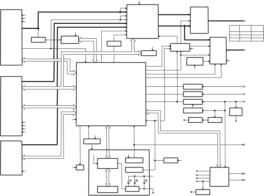
TUNER |
AM+B |
|
|
|
SW5V |
|
A8V |
AUDIO OUT |
|
BUFFER
S-METER
PLL-DATA
PLL-CLK
IFC OUT
MP3
MS DATA
MS CLK
LO/S SW(SW1) 12EJE SW(SW2) SW(SW3) LO.E/LIM M MUTE M RST
MSTOP LO/EJ
SERVO+B
A8V
BU5V
MECHA+
CH
REQ C
CH CLK
DATA H
CH-CON
REQ H
DATA C
CH RST
CH MUTE
BACK UP
SW5V
IC7
RDS
DECODER BUFFER
IC1
METER- |
RDATA RCLK QUAL |
S |
|
DATA
CLK
u-COM
DSI |
TDFDET |
DATASL CLKL CEL DATALL |
BU5V |
|
|
|
|
A8V |
|
IC2 |
|
|
|
FM |
|
|
|
AM |
|
|
|
MP |
|
E-VOL |
|
LEVEL |
|||
& |
|||
CD |
|
||
|
MPX |
||
|
|
||
CH |
|
|
|
AFS |
|
|
|
QUAL |
|
||
|
|
SW5V |
|
|
|
EEPROM |
|
|
|
MUTE |
|
|
P-MUTE |
||
|
|
BEEP |
|
|
|
P-STBY |
|
|
|
PHONE |
|
|
ACC DET |
||
|
B.U DET |
||
|
|
PS1-0 |
|
|
|
PS1-1 |
|
|
|
PS1-2 |
|
|
|
PS2-0 |
|
|
REMO |
PS2-2 |
|
|
RST |
||
|
|
||
|
|
PRE MUTE |
|
|
PRE OUT |
|
|
|
|
|
(REAR) |
||
|
|
|
|
|
||
|
|
|
|
MODE |
K-TYPE |
E-TYPE |
|
|
|
IC4 |
FM |
1800mV |
1372mV |
|
|
|
AM |
600mV |
855mV |
|
|
|
|
|
|||
|
|
|
|
MP3 |
3600mV |
3600mV |
MUTE |
|
|
|
|
|
|
DRIVER |
BU5V |
POWER |
|
SP OUT |
||
|
|
|||||
|
|
|
IC |
|
||
|
|
|
|
|
|
|
|
|
THERMAL |
|
BACK UP |
|
|
|
|
PROTECT |
|
|
||
|
|
|
|
|
|
|
|
|
SW5V |
|
|
|
|
|
|
TEL MUTE |
|
|
TEL MUTE |
|
|
|
ACC DET |
|
|
ACC |
|
|
|
B.U DET |
|
|
BACK UP |
|
|
SURGE DET |
|
MECHA |
|
||
|
|
|
|
+B |
|
|
SERVO+B |
|
SERVO |
SW 14V |
|
|
|
|
|
|
|
MECHA+ |
|
|
BU5V
PANEL 5V WIRED REMO
BU5V
|
PANEL |
SW5V |
|
|
IC1 |
IC2 |
IC8 |
|
|
|
|
|
LCD DRIVER |
REMOCON |
RESET |
|
WITH |
|
|
DSI |
KEY MATRIX |
|
|
|
RESET SW |
|
|
|
|
|
|
|
|
|
ILLUMI |
BU5V
AM+B
A8V
ILLUMI
BU5V
IC3 |
|
POWER |
ANT CON |
SUPPLY |
|
IC |
P CON |
LCD |
ILL SW |
|
SW5V |
SW 5V |
BLOCK |
M4524/G/Y/GY-KDC |
DIAGRAM |
|
SWITCH UNIT (X16- )
KDC-M4524/G/Y/GY
COMPONENTS DESCRIPTION
● SWITCH UNIT (X16-2052-71/2362-70)
Ref. No. |
Function |
Operation |
|
|
|
IC1 |
LCD Driver |
|
|
|
|
IC2 |
Remote-control IC |
|
|
|
|
Q1 |
Key-scan Start SW |
"ON" when the base goes "L". |
|
|
|
Q2 |
Key-illuminations SW (GREEN) |
ON (Key-illuminations Green) when the base goes "H". |
|
|
|
Q3 |
Key-illuminations SW (RED) |
ON (Key-illuminations RED) when the base goes "H". |
|
|
|
● ELECTRIC UNIT (X25-9622-71/9812-70)
Ref. No. |
Function |
Operation |
|
|
|
|
|
IC1 |
System MI-COM |
|
|
|
|
|
|
IC2 |
E-VOL. & N.C. MPX |
|
|
|
|
|
|
IC3 |
Power Supply IC |
|
|
|
|
|
|
IC4 |
Power IC |
|
|
|
|
|
|
IC6 |
Analog SW (Mute logic) |
|
|
|
|
|
|
IC7 |
RDS Demodulator |
|
|
|
|
|
|
IC8 |
Reset IC |
“L” : detection voltage below 3.6V |
|
|
|
|
|
IC9 |
CD mechanism 5V AVR |
|
|
|
|
|
|
Q1 |
SERGE Det. |
ON when the base goes “Hi”. |
|
|
|
|
|
Q2 |
B.U. Det. |
ON when the base goes “Hi” during BU applied. |
|
|
|
|
|
Q3 |
ACC Det. |
ON when the base goes “Hi” during ACC applied. |
|
|
|
|
|
Q4 |
SW 5V |
ON when the base goes “Lo”. |
|
|
|
|
|
Q21 |
SERVO +B AVR |
Output voltage 7.4V |
|
|
|
|
|
Q22 |
SW 14V |
ON when the base goes “Hi”. |
|
|
|
|
|
Q41 |
MECHA 5V AVR SW |
ON when the base goes “Lo”. |
|
|
|
|
|
Q101 |
Buffer |
The buffer for composite signals. |
|
|
|
|
|
Q151 |
Panel 5V SW |
ON when the base goes “Lo”. |
|
|
|
|
|
Q201 |
Noise buffer |
|
|
|
|
|
|
Q350 |
Mute driver for Audio mute SW |
ON when the base goes “Lo”. |
|
|
|
|
|
Q351 |
Pre mute SW |
Audio Pre-output is muted when the base goes “Hi”. |
|
|
|
||
Q352 |
Pre mute SW |
||
|
|||
|
|
|
|
Q401 |
DSI ILLUMI SW |
ON when the base goes “Lo”. |
|
|
|
|
3
KDC-M4524/G/Y/GY
MICROCOMPUTER’S TERMINAL DESCRIPTION
● SYSTEM MICROCOMPUTER UPD703030GC011 (IC1 : X25)
pin |
pin name |
I/O |
Description |
truth table |
Processing Operation |
|
|
|
|
|
|
1 |
PLL CLK |
I/O |
Clock output to F/E |
|
|
|
|
|
|
|
|
2 |
AFS |
O |
Noise detection time constant switching terminal |
|
FM seek/during/AF search : L, receiving : H |
|
|
|
|
|
|
3 |
TDF DET |
I |
TDF panel detection terminal |
|
Panel detached : H, panel attached : L |
|
|
|
|
|
|
4 |
IC2 SDA |
I/O |
Data input and output terminal with E-VOL |
|
|
|
|
|
|
|
|
4 |
IC2 SDA |
I/O |
Data input and output terminal with CD mechanism |
|
|
|
|
|
|
|
|
4 |
IC2 SDA |
I/O |
Data input and output terminal with E2PROM |
|
|
|
|
|
|
|
|
5 |
IC2 SCL |
I/O |
Clock output to E-VOL |
|
|
|
|
|
|
|
|
5 |
IC2 SCL |
I/O |
Clock output to CD mechanism |
|
|
|
|
|
|
|
|
5 |
IC2 SCL |
I/O |
Clock output to E2PROM |
|
|
|
|
|
|
|
|
6 |
VDD |
- |
|
|
|
|
|
|
|
|
|
7 |
VSS |
- |
|
|
|
|
|
|
|
|
|
8 |
- |
O |
Not used |
|
|
|
|
|
|
|
|
9 |
BEEP |
O |
Beep output terminal |
|
|
|
|
|
|
|
|
10 |
REMO |
I |
Remote control input |
|
|
|
|
|
|
|
|
11 |
R QUAL |
I |
RDS decoder quality input terminal |
|
|
|
|
|
|
|
|
11 |
- |
O |
Not used |
|
With no RDS and destination is output L |
|
|
|
|
|
|
12 |
R DATA |
I |
RDS decoder data input terminal |
|
|
|
|
|
|
|
|
12 |
- |
O |
Not used |
|
With no RDS and destination is output L |
|
|
|
|
|
|
13 |
L CE |
O |
CE output to LCD driver |
|
|
|
|
|
|
|
|
14 |
- |
O |
Not used |
|
|
|
|
|
|
|
|
15 |
L INH |
O |
Reset output to LCD driver |
|
Display light off, KEY reset : L Display light on, |
|
KEY scan : H |
||||
|
|
|
|
|
|
|
|
|
|
|
|
16 |
DSI |
O |
DSI control terminal |
|
DSI light on : H, Light off : L |
|
|
|
|
|
|
17 |
- |
O |
Not used |
|
|
|
|
|
|
|
|
18 |
TEST |
- |
|
|
|
|
|
|
|
|
|
19~21 |
- |
O |
Not used |
|
|
|
|
|
|
|
|
22 |
MOSW |
O |
CD mechanism motor IC switch |
e |
Loading/Eject/Break : H |
|
|
|
|
|
|
23 |
LO/EJ |
I/O |
CD mechanism Loading/Eject switch |
e |
Stop/Break : Hi-Z Loading : L Eject : H |
|
|
|
|
|
|
24 |
M STOP |
O |
Stop request to CD mechanism |
|
|
|
|
|
|
|
|
25 |
M RST |
O |
Reset output to CD mechanism |
|
Usually : H, Reset : L |
|
|
|
|
|
|
26 |
MUTE |
I/O |
Mute terminal |
|
L : MUTE OFF, H : MUTE ON |
|
|
|
|
|
|
27 |
LO.E/LIM SW (SW3) |
I |
CD Down Switch detection terminal |
|
H : chucking |
|
|
|
|
|
|
28 |
M MUTE L |
I |
MUTE request from CD mechanism |
|
L : MUTE request |
|
|
|
|
|
|
29 |
M MUTE R |
I |
MUTE request from CD mechanism |
|
L : MUTE request |
|
|
|
|
|
|
30 |
- |
O |
Not used |
|
|
|
|
|
|
|
|
31 |
RESET |
I |
|
|
Usually : H, Reset : L |
|
|
|
|
|
|
32 |
XT1 |
I |
Sub clock 32.765kHz |
|
|
|
|
|
|
|
|
33 |
XT2 |
I |
Sub clock 32.765kHz |
|
|
|
|
|
|
|
|
34 |
REGC |
- |
|
|
Ceramic capacitor connected to the pair grounds |
|
|
|
|
|
|
35 |
X2 |
I |
Main clock 20MHz |
|
|
|
|
|
|
|
|
36 |
X1 |
I |
Main clock 20MHz |
|
|
|
|
|
|
|
|
37 |
VSS |
- |
|
|
|
|
|
|
|
|
|
38 |
VDD |
- |
|
|
|
|
|
|
|
|
|
39 |
CLKOUT |
- |
|
|
|
|
|
|
|
|
|
40 |
IC2 TYPE1 |
I |
E-VOL setting switching terminal |
|
|
|
|
|
|
|
|
41 |
IC2 TYPE0 |
I |
E-VOL setting switching terminal |
|
|
|
|
|
|
|
|
42 |
- |
O |
Not used |
|
|
|
|
|
|
|
|
43 |
TYPE1 |
I |
Destination switching terminal |
r |
|
|
|
|
|
|
|
44 |
TYPE0 |
I |
Destination switching terminal |
r |
|
|
|
|
|
|
|
4
KDC-M4524/G/Y/GY
MICROCOMPUTER’S TERMINAL DESCRIPTION
pin |
pin name |
I/O |
Description |
truth table |
Processing Operation |
|
|
|
|
|
|
45 |
CD MECHA+B |
I/O |
Power supply control terminal for MP3 |
|
ON : L, OFF : Hi-Z |
|
|
|
|
|
|
46 |
SW5V |
I/O |
Control terminal for switch5V |
|
ON : L, OFF : Hi-Z |
|
|
|
|
|
|
47 |
PS2-0 |
O |
Control terminal for power supply IC |
w |
|
|
|
|
|
|
|
48 |
PS2-1 |
O |
Control terminal for power supply IC |
w |
|
|
|
|
|
|
|
49 |
PS1-0 |
O |
Control terminal for power supply IC |
q |
|
|
|
|
|
|
|
50 |
PS1-1 |
O |
Control terminal for power supply IC |
q |
|
|
|
|
|
|
|
51 |
PS1-2 |
O |
Control terminal for power supply IC |
q |
|
|
|
|
|
|
|
52 |
BU DET |
I |
BU detection terminal |
|
BU detection : L, with no BU : H |
|
|
|
|
|
|
53 |
ACC DET |
I |
ACC detection terminal |
|
ACC detection : L, with no ACC : H |
|
|
|
|
|
|
54 |
- |
O |
Not used |
|
|
|
|
|
|
|
|
55 |
BVDD |
- |
|
|
|
|
|
|
|
|
|
56 |
BVSS |
- |
|
|
|
|
|
|
|
|
|
57,58 |
- |
O |
Not used |
|
|
|
|
|
|
|
|
59 |
P-MUTE |
O |
POWER IC MUTE output terminal |
|
POWER OFF : L, ALLOFF : L, TEL MUTE : L |
|
|
|
|
|
|
60 |
P-STBY |
O |
POWER IC STBY output terminal |
|
POWER IC ON : H, OFF : L |
|
|
|
|
|
|
61,62 |
- |
O |
Not used |
|
|
|
|
|
|
|
|
63 |
PRE MUTE |
O |
PREOUT MUTE output |
|
during momentary power down L, |
|
When M-MUTEL : L |
||||
|
|
|
|
|
|
|
|
|
|
|
|
64~67 |
- |
O |
Not used |
|
|
|
|
|
|
|
|
68 |
LX-RST |
O |
Reset output to external unit |
|
Usually, L after system RST returned,after |
|
more than 400m sec H,and L |
||||
|
|
|
|
|
|
|
|
|
|
|
|
69 |
LX-CON |
O |
Control output to external unit |
|
ON : H, OFF : L |
|
|
|
|
|
|
70 |
AVCONT |
O |
AD reference voltage control output |
|
during motion : H |
|
|
|
|
|
|
71 |
AVDD |
- |
|
|
|
|
|
|
|
|
|
72 |
AVSS |
- |
|
|
|
|
|
|
|
|
|
73 |
AVREF |
- |
|
|
Connection with 70pin |
|
|
|
|
|
|
74 |
PHONE |
I |
PHONE detection terminal |
|
TEL MUTE : 1V orless, NAVI MUTE : more |
|
than 2.5V |
||||
|
|
|
|
|
|
|
|
|
|
|
|
74 |
- |
I |
Not used (with no PHONE destination) |
|
|
|
|
|
|
|
|
75~81 |
- |
I |
Not used |
|
|
|
|
|
|
|
|
82 |
S-METER |
I |
S-meter detection terminal |
|
Dependant for control use of tuner |
|
|
|
|
|
|
83 |
NOISE |
I |
FM noise detection terminal |
|
Dependant for control use of tuner |
|
|
|
|
|
|
84 |
IFC-OUT |
I |
F/E IFC OUT input terminal |
|
Dependant for control use of tuner |
|
|
|
|
|
|
85 |
LX-MUTE |
I |
MUTE request to external unit |
|
H : MUTE ON, L : MUTE OFF |
|
|
|
|
|
|
86 |
LX-REQM |
O |
Request output to external unit |
|
Request detection : L |
|
|
|
|
|
|
87 |
R CLK |
I |
RDS decoder Clock input terminal |
|
|
|
|
|
|
|
|
87 |
- |
O |
Not used |
|
Destination with no RDS : output L fixed |
|
|
|
|
|
|
88 |
LX-REQS |
I |
Request intput to external unit |
|
Request detection : L |
|
|
|
|
|
|
89 |
KEY-REQ |
I |
Request of communication from LCD driver |
|
L : KEY input |
|
|
|
|
|
|
90 |
LO.S SW (SW1) |
I |
Loading start switch detection terminal |
|
Loading start : L |
|
|
|
|
|
|
91 |
12EJE SW (SW2) |
I |
12cmDISK EJECT position detection switch terminal |
|
12cmDISC : L |
|
|
|
|
|
|
92 |
- |
O |
Not used |
|
|
|
|
|
|
|
|
93 |
- |
O |
Not used |
|
|
|
|
|
|
|
|
94 |
LX-DATAS |
I |
Data input from external unit |
|
|
|
|
|
|
|
|
95 |
LX-DATAM |
O |
Data output to external unit |
|
Holding the last |
|
|
|
|
|
|
96 |
LX-CLK |
I/O |
Clock output and input terminal with external unit |
|
|
|
|
|
|
|
|
97 |
L DATAL |
I |
Data input from LCD driver |
|
|
|
|
|
|
|
|
98 |
L DATAS |
O |
Data output to LCD driver |
|
|
|
|
|
|
|
|
99 |
L-CLK |
I/O |
Clock output to LCD driver |
|
|
|
|
|
|
|
|
100 |
PLL DATA |
I/O |
Data output and input terminal with F/E |
|
|
|
|
|
|
|
|
5
KDC-M4524/G/Y/GY
MICROCOMPUTER’S TERMINAL DESCRIPTION
Truth table 1
PS1-0 |
PS1-1 |
|
|
|
PS1-2 |
|
|
AUDIO |
|
P-CON |
|
P-ANT |
|||||
|
|
|
|
|
|
|
|
|
|
|
|
|
|
|
|
|
|
L |
L |
|
|
|
L |
|
|
OFF |
|
OFF |
|
OFF |
|||||
|
|
|
|
|
|
|
|
|
|
|
|
|
|
|
|
|
|
H(L) |
L(H) |
|
|
|
L |
|
|
ON |
|
OFF |
|
OFF |
|||||
|
|
|
|
|
|
|
|
|
|
|
|
|
|
|
|
|
|
H |
H |
|
|
|
L |
|
|
ON |
|
ON |
|
OFF |
|||||
|
|
|
|
|
|
|
|
|
|
|
|
|
|
|
|
|
|
H |
H |
|
|
|
H |
|
|
ON |
|
ON |
|
ON |
|||||
|
|
|
|
|
|
|
|
|
|
|
|
|
|
|
|
|
|
Truth table 2 |
|
|
|
|
|
|
|
|
|
|
|
|
|
|
|
|
|
|
|
|
|
|
|
|
|
|
|
|
|
|
|
|
|
||
PS2-0 |
PS2-1 |
|
|
|
ILLUMI |
|
FM+B |
|
AM+B |
|
|
|
|||||
|
|
|
|
|
|
|
|
|
|
|
|
|
|
|
|
|
|
L |
L |
|
|
|
OFF |
|
OFF |
|
OFF |
|
|
|
|||||
|
|
|
|
|
|
|
|
|
|
|
|
|
|
|
|
|
|
H (L) |
L (H) |
|
|
|
ON |
|
ON |
|
OFF |
|
|
|
|||||
|
|
|
|
|
|
|
|
|
|
|
|
|
|
|
|
|
|
H |
H |
|
|
|
ON |
|
OFF |
|
ON |
|
|
|
|||||
|
|
|
|
|
|
|
|
|
|
|
|
|
|
|
|
|
|
Truth table 3 |
|
|
|
|
|
|
|
|
|
|
|
|
|
|
|
|
|
|
|
|
|
|
|
|
|
|
|
|
|
|
|
|
|||
MOSW |
LO/EJ |
|
|
|
CD mechanism operation |
|
|
|
|
|
|
||||||
|
|
|
|
|
|
|
|
|
|
|
|
|
|
|
|
|
|
L |
H |
|
|
|
|
Load |
|
|
|
|
|
|
|
|
|||
|
|
|
|
|
|
|
|
|
|
|
|
|
|
|
|
|
|
H |
H |
|
|
|
|
Eject |
|
|
|
|
|
|
|
|
|||
|
|
|
|
|
|
|
|
|
|
|
|
|
|
|
|
|
|
- |
L |
|
|
|
|
Lo/Ej invalid truth |
|
|
|
|
|
|
|||||
|
|
|
|
|
|
|
|
|
|
|
|
|
|
|
|
|
|
Hi-Z |
H |
|
|
|
|
Brake |
|
|
|
|
|
|
|
|
|||
|
|
|
|
|
|
|
|
|
|
|
|
|
|
|
|
|
|
Truth table 4 (destination setting) |
|
|
|
|
|
|
|
|
|
|
|
|
|||||
|
|
|
|
|
|
|
|
|
|
|
|
|
|
|
|
||
model |
|
destination |
|
|
|
destination ports |
|
|
|
||||||||
|
|
|
|
|
|
|
|
|
|
||||||||
TYPE2 |
|
TYPE1 |
|
|
TYPE0 |
|
|||||||||||
|
|
|
|
|
|
|
|
|
|
|
|||||||
|
|
|
|
|
|
|
|
|
|
|
|
|
|
|
|||
KDC-MP222 |
|
|
K |
|
- |
|
|
0 |
|
|
|
0 |
|
|
|||
|
|
|
|
|
|
|
|
|
|
|
|
|
|
|
|||
KDC-MP4023 |
|
|
M (E) |
|
- |
|
|
0 |
|
|
|
1 |
|
|
|||
|
|
|
|
|
|
|
|
|
|
|
|
|
|
||||
KDC-M4524/G/Y/GY |
|
E/E2 |
|
- |
|
|
1 |
|
|
|
0 |
|
|
||||
|
|
|
|
|
|
|
|
|
|
|
|
|
|
|
|
|
|
TEST MODE
1.How to enter the test mode
While holding the Preset 1 and Preset 3 keys, reset the unit.
2.How to exit from the test mode
Reset the unit, ACC OFF, power OFF and Panel detached. (Note) The test mode cannot be terminated by momen-
tary power down.
3.Initial status in the test mode
• Sources |
: ALL OFF |
• Display |
: All segments are lit. |
• Volume |
: -10 dB (displayed as "30") |
• Loudness |
: OFF |
• CRSC |
: OFF regardless of the presence of |
|
switching function. |
• SYSTEM Q |
: Flat |
• BEEP |
: When pressing any keys, the buzzer |
|
generates a beep at any time. |
•SYSTEM Q MENU : OFF
4.Special display in Tuner mode
When any of the following messages is displayed in Tuner mode, the F/E may be abnormal.
•"TNE2P NG" : The EEPROM is set to the default (unstable values) because the F/E was shipped without passing through the adjustment process, etc.
•"TNCON NG" : Communication with the F/E is not possible.
6

KDC-M4524/G/Y/GY
TEST MODE
5. Forced switching of K3I
Each press of the Preset 6 key in Tuner mode should switch K3I from AUTO → Forced Wide → Forced Middle → Forced Narrow → AUTO.
The initial status is AUTO and the display shows these
modes as follows. |
|
• AUTO |
: FMA |
• Forced Wide |
: FMW |
• Forced Middle |
: FMM |
• Forced Narrow |
: FMN |
6.Test mode specifications of the CD receiver
•Forced ejection is inhibited in the reset start operation. When the unit is reset while a CD is loaded in it, the CD is not recognized by resetting.
•Each press of the Track Up key jumps to the following
track numbers:
No. 9 → No. 15 → No. 10 → No. 11 → No. 12 → No.13 → No. 14 → No. 9 (The cycle restarts from here.)
•Each press of the Track Down key jumps to the previous track number to the track being played.
•When the number of total trucks of the MP3 disc is less than 9, 1st truck is played.
•When the disc media is CD, a short press of the Preset 1 key jumps to the track number 28.
7.Audio-related specifications
•A short press of the Q key initiates the audio adjustment mode.
•Pressing the key on the remote initiates the audio adjustment mode.
•Fader is selected to the initial item.
•Continuous holding of a remote control key is inhibited.
•Bass, Middle and Treble are adjusted in 3 steps of Min/ Center/Max with the Track Up/Down keys.
•Balance is adjusted in 3 steps of Left Max/Center/Right Max with the Track Up/Down keys.
•Fader is adjusted in 3 steps of Rear Max/Center/Front Max with the Track Up/Down keys.
•Bass f/Bass Q/Bass EXT/Middle f/Middle Q/Treble f are not death with by the audio adjust.
8.Menu-related specifications
•A short press of the PLAY/PAUSE key initiates the Menu mode.
•Pressing the DNPP/SBF key on the remote initiates the Menu mode.
•Continuous holding of a remote control key is inhibited, a short press initiates the Menumode.
•Contrast is adjusted in 3 steps of 0/5/10, with the trackup/ down keys.
9.Backup current measurement
When the unit is reset while ACC is OFF (i.e. by turning Backup ON), the MUTE terminal goes OFF in 2 seconds in place of 15 second. (The CD mechanism is not activated at this time.)
10.Special display when the display is all on
Pressing the Preset keys while the power is ALL OFF displays the following information.
Version display
PRESET 1 (8 digits, Month/Day/Hour/Minute)
(Display) SYSxxxxx : System microcomputer
Short press : View power ON time. (The All OFF period is not counted.)
PRESET 3 Long press/hold : Clear power ON time at the power ON time displaying.
(Display) PonTim xxxxx Max. 60000 (hours)
Short press : Display CD operation time.
Long press/hold : Clear CD operation time at
PRESET 4
the CD operation time displaying. (Display) CDTimxxxxx Max. 60000 (hours)
Short press : Display CD ejection count.
Long press/hold : Clear CD ejection count at
PRESET 5
the CD ejection count displaying.
(Display) EjeCnt xxxxx Max. 60000 (times)
Short press : Display Panel open/close count.
Long press/hold : Clear Panel open/close
PRESET 6
count at the Panel open/close count. (Display) PnCnt xxxxx Max. 600000 (times)
11.Other specifications
LINE MUTE inhibit time is 1 second from 10 second when start up the test mode.
12.Switching the frequency span (K/M type)
While holding the preset q key and preset t keys, reset the unit.
13.Response to OEM setting (destination of electronic volume setting)
S03F/E models are response to OEM models option at put in µ -com 2 pin.
Its setting re following steps.
IC2-TYPE0 |
IC2-TYPE1 |
Description |
|
(41pin) |
(40pin) |
||
|
|||
|
|
|
|
Low |
Low |
qTrade model (initial quantif) |
|
|
|
|
|
Low |
High |
wTrade model (CRSC Change) |
|
|
|
|
|
High |
Low |
eOEM model-ready CRSC change |
|
|
|
|
|
High |
High |
rOEM model-ready CRSC & |
|
de-emphasis |
|||
|
|
7

A |
B |
C |
D |
E |
|
KDC-M4524/G/Y/GY |
|
1 |
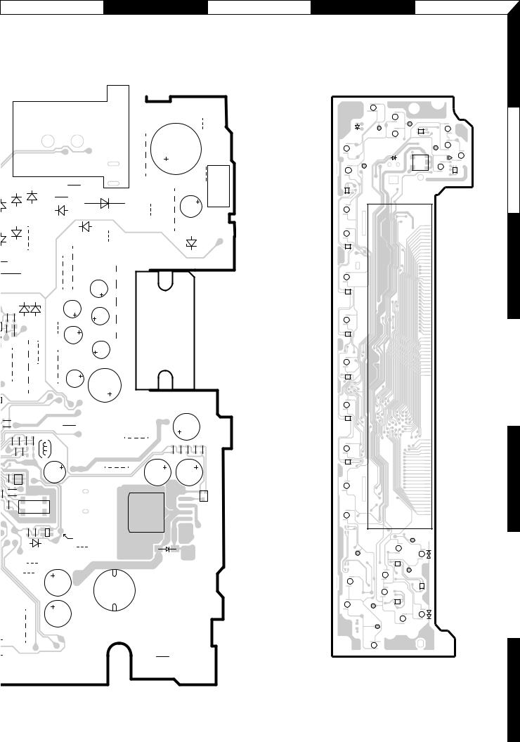
PC BOARD (COMPONENT SIDE VIEW) |
|
|
ELECTRIC UNIT (X25-9622-71/9812-70) (J74-1466-12) |
▼ |
|
|
|
2
J4
3
L3
A1
1
4
5
24
6
7
8
|
|
|
|
|
|
|
|
|
|
|
|
|
|
|
|
W3 |
|
|
W6 |
W9 |
|
|
|
|
|
|
|
|
|
|
|
|
|
J2 |
|
|
|
|
|
|
|
|
W4 |
|
W7 |
|
|
|
|
|
|
||
|
|
|
|
|
|
|
|
|
|
|
|
|
|
|
|
|
|
|
|
|
|
|
||||
|
|
|
|
|
|
|
|
|
|
|
|
|
|
|
|
|
|
|
IC4 |
|
|
|
|
|
|
9 |
|
|
J3 |
|
|
|
|
|
|
|
|
|
|
|
|
|
|
|
|
|
|
|
|
|
|
|
|
|
|
|
|
|
|
|
|
|
|
|
|
|
|
|
|
2 |
|
|
24 |
|
|
|
|
|
8 |
|
|
|
|
|
|
13 11 12 |
8 |
4 |
3 |
2 |
|
|
|
|
|
|
|
|
|
|
D255 |
|
|||||
|
|
|
|
|
9 |
10 |
6 |
7 |
|
5 |
1 |
|
|
|
|
|
1 |
|
|
25 |
|
|
|
D251 |
||
|
|
|
|
|
|
|
|
|
|
|
|
|
|
|
|
|
|
|
||||||||
|
|
|
|
|
|
|
|
|
|
|
|
|
|
|
|
|
|
|
|
|
|
|
|
|
||
|
|
|
|
|
|
|
|
|
|
|
|
|
|
|
|
|
|
W5 |
W8 |
|
|
|
|
|
|
|
R356 |
R358 |
R355 R351 |
R357 |
R302 |
R306 |
R301 |
R308 |
R311 |
|
R309 |
R310 |
R307 |
R304 |
R305 |
R303 |
D301 |
|
|
|
|
|
W10 |
W11 |
D252 |
D254 |
|
W1 |
R352 |
Q350 |
|
D311 |
|
|
|
C302 |
|
|
|
|
D304 |
|
C253 |
C251 |
C255 |
C257 |
|
|
|
|
|
|
||
|
|
|
|
|
|
|
|
|
|
|
|
|
|
D303 |
|
|
|
|
|
C258 |
|
|
|
|
|
|
|
BE |
|
|
D310 |
|
|
|
|
|
|
|
|
|
D302 |
|
|
|
|
|
|
|
|
R31 |
|
|
|
|
|
|
|
|
|
|
|
|
|
|
|
|
|
|
|
|
|
|
|
|
|
|
|
|
||
|
|
|
|
|
|
|
|
|
|
|
|
|
|
|
|
|
|
|
|
|
|
|
|
R8 |
|
|
|
|
|
|
D309 |
|
|
|
|
|
|
C303 |
|
|
|
D307 |
|
|
|
|
|
|
|
|
|
|
|
|
+ |
|
|
|
|
|
D206 |
|
|
|
|
|
|
|
D306 |
|
|
|
|
|
|
|
|
|
|
|
|
|
|
|
|
|
|
|
|
|
C301 |
|
D308 |
C254 |
C252 |
C256 |
D269 |
D270 |
D271 |
|
R6 |
C3 |
D2 |
||||
|
|
|
|
|
|
|
|
|
|
|
|
|
|
|
|
|
|
|
|
|
D31 |
|
|
|||
|
C352 |
|
|
|
|
|
D203 |
|
|
|
|
|
|
|
D305 |
|
|
|
|
|
|
|
|
|
|
|
|
|
|
|
|
|
|
|
|
|
|
|
|
|
|
|
|
|
|
|
|
|
|
|
|
|
|
|
|
C351 |
|
|
|
|
|
|
|
|
|
|
|
|
|
|
|
|
R256 |
|
|
|
Q2 |
|
|
|
|
|
|
|
|
|
|
|
|
|
|
|
|
|
|
|
|
|
|
R255 |
R9 |
D4 |
|
BE |
R5 |
R4 |
|
|
|
|
|
|
|
|
|
|
|
|
|
|
|
|
|
|
|
|
|
|
R10 C4 |
|
R7 |
|
|
|
|
|
|
|
|
|
|
|
|
|
|
|
|
|
|
|
|
|
|
|
|
|
|
|
|
||
C115
C118 C114
8
IC7
L10 |
14 |
8 |
R317 |
|
|
C309 |
|
|
|
IC6 |
|
|
C211 |
|
|
||
L5 |
C210 |
NOISE 1 |
|
||
28 |
15 |
7 |
|||
|
L8 L7 L6 W2
IC2
|
1 |
|
|
C203 |
C205 |
C212 |
|
|
|
|
|
|
|
14 |
|
||
|
|
|
|
|
|
C206 |
|
|
C201 |
D201 |
D202 |
C202 |
R201 |
R202 |
C204 |
C213 |
|
R203 |
||||||||
|
|
|
|
|
|
|
CN4
1
2
|
SMETER |
|
8 |
5 |
|
|
IC10 |
IFC |
|
|
|
1 |
4 |
R101 |
|
||
SCL
SDA
R315 |
C111 |
R401 |
R405 |
R406 |
|
C304 |
R404 |
R402 |
75 |
||
|
|
76 |
|||
R106 |
R403 |
|
|||
|
|
|
|
||
|
R52 R51 |
|
|||
|
|
|
R153 |
|
|
R154 |
|
R152 |
|
||
|
|
100 |
|||
R102 |
|
|
|
1 |
|
|
|
|
|
||
R104 |
|
|
|
|
|
R206 |
|
|
|
|
|
C116 |
|
|
|
D52 |
R207 |
R208 |
C117 |
|
R374 |
D152 |
|||
|
|
|
||||
|
|
|
|
|||
|
|
|
D153 |
D51 |
|
|
|
|
|
|
|
|
|
|
R112 |
D151 |
D154 |
|
|
|
1 |
D160 |
|
|
|
|
|
R113 |
D157 |
|
2 |
|
||
|
R114 |
|
|
|
|
|
|
D161 |
D158 |
|
CN2 |
|
|
|
|
D162 |
D155 |
|
1 |
|
|
|
|
|
|
|
Q3 |
EB |
|
|
C5 |
|
|
|
|
|
|
|
W12 |
|
W17 |
|
|
|
|
|
|
|
|
|
|
|
|
|
|
||||
R251 |
|
R11 |
|
|
|
|
|
|
|
|
||||||
|
|
|
|
|
|
|
|
|
|
|
|
|||||
|
|
|
|
Q23 |
|
|
D26 |
|
|
|
|
|
||||
|
|
|
|
|
EBE |
|
|
|
|
|
|
|
|
|
|
|
|
|
|
|
|
|
R25 |
R26 |
|
R27 |
|
|
|
||||
|
|
|
|
|
|
|
|
|
|
|
|
|
|
|
|
|
|
|
|
|
|
|
|
|
|
|
|
|
R28 |
|
|
|
|
|
|
|
|
|
R24 |
50 |
|
|
|
R417 |
|
R411 |
||||
|
|
|
|
|
|
|
|
|
R412 |
|
||||||
|
|
|
|
|
|
|
|
|
|
|
|
|
|
R415 |
|
|
|
IC1 |
|
|
|
|
|
|
|
|
|
|
|
|
R419 |
||
|
|
|
|
|
|
|
|
|
|
|
|
|
|
|
|
|
|
|
|
|
|
|
|
|
|
R420 |
|
R409 |
X1 |
|
|
||
|
|
|
|
|
|
26 |
|
|
C40 |
|||||||
|
|
|
|
25 |
|
|
|
|
|
|
|
C40 |
||||
|
|
R59 |
|
R55 |
R54 |
|
|
|
|
C407 |
|
|
|
|||
R160 |
|
R60 |
|
R56 |
R58 |
|
|
R53 |
|
|
|
|
R410 |
|||
|
R63 |
|
|
|
|
|
|
|||||||||
|
|
|
|
|
|
|
|
|
|
|
|
|
|
|
||
|
|
|
|
|
|
R62 |
R61 |
|
|
|
|
|
||||
TEST
RST
24
W
23
9 |
16 |
|
|
|
|
|
|
|
|
P1 |
|
|
X3 |
D159 |
R172 |
R183 |
R175 |
R173 |
R171 |
R174 |
R180 |
R182 |
D156 |
|
W15 |
|
|
|
|
|
|
|
|
|
|
|
|
R181 |
|
|
|
|
|
|
14 |
|
|
|
|
2 |
R176 |
|
|
|
|
|
|
15 |
|
|
|
|
|
|
|
|
|
|
|
|
|
|
|
|
|
1 |
|
|
|
|
|
|
|
|
|
|
|
J5 |
|
|
▲
F |
G |
H |
I |
J |
|
|
|
KDC-M4524/G/Y/GY |
|
1
▼ |
|
|
SWITCH UNIT |
|
|
|
|
|
|
|
X16-2052-71/2362-70 (J74-1464-02) |
|
|
|
|
|
|
|
J1 |
|
|
W30 |
|
|
|
|
|
|
|
|
|
|
|
|
L1 |
W28 |
|
|
|
|
|
9 |
16 |
|
|
|
|
|
|
|
|
|
|
||
|
|
8 |
1 |
|
|
W31 |
B E |
D255 |
D251 |
D253 |
R22 |
|
C1 |
||
|
|
|
|
|
|
|
|
D252 |
D254 |
|
R23 |
|
|
|
|
W16 |
W25 |
W32 |
W29 |
|
Q21 |
||
|
|
|
D1 |
|
|
|
|
D23 |
▲ |
C21 |
|
||
|
|
|
|
D22 |
|
1 |
|
W23 |
R8 |
W21 |
|
|
|
|
|
D2 |
D3 |
|
|
C23 |
R6 |
C3 |
|
|
|
|
|
|
R5 |
R4 |
|
|
|
W19 |
|
|
|
|
|
|
W18 |
|
|
C24 |
W12 |
|
|
W17 |
|
W20 |
|
|
|
|
|
|
GND |
|
C26 |
|
|
|
|
|
|
|
|
|
R27 |
|
|
|
|
|
|
|
R28 |
|
R417 |
R411 |
R416 |
|
L11 |
R13 |
R412 |
|
|
|||||
|
|
R415 |
R419 |
|
|
|
C409 |
|
|
|
|
|
|
|
|
R409 |
|
X1 |
|
|
|
|
|
|
|
C405 |
|
|
|
||
|
|
C408 |
|
|
|
||
C407 |
|
|
|
X2 |
|
|
|
|
|
|
C406 |
IC8 |
|
||
|
|
|
R410 |
VDD |
|||
|
|
|
2 |
3 |
|||
|
|
|
|
|
1 |
4 |
|
|
|
|
|
D401 |
|
W22 |
|
RST |
|
|
|
|
|
|
|
|
|
|
W14 |
|
|
|
|
|
|
|
W13 |
|
|
C43 |
|
|
|
|
|
|
|
|
|
|
|
|
|
|
|
|
C44 |
1 |
|
W15 |
|
|
|
|
|
|
|
|
|
|
|
|
|
6 |
|
|
|
|
|
|
|
|
|
|
D21 |
|
|
|
C22 |
1 |
|
|
|
|
|
|
W26 |
|
|
|
|
|
C29 |
IC3 |
|
|
|
|
|
C25 |
|
|
|
|
|
|
|
12 |
|
|
|
|
|
C28 |
|
C27 |
|
|
|
|
|
|
|
|
|
||
|
W27 |
|
|
|
|
|
|
R44 |
R43 |
C45 |
R41 |
R42 |
|
|
W24 |
|
|
|
|
|
|
C41 |
C42 |
EB |
Q41 |
||
|
|
5 |
|
|||
|
|
|
|
|
||
|
IC9 |
|
|
|
|
|
|
|
1 |
|
|
|
|
D41
L12
R407
ELECTRIC UNIT (X25-9622-71/9812-70)
IC |
Q |
Address |
|
|
|
1 |
|
5E |
2 |
|
4C |
3 |
|
4G |
4 |
|
2D |
6 |
|
4D |
8 |
|
5F |
9 |
|
5G |
|
2 |
4E |
|
3 |
4E |
|
21 |
2H |
|
23 |
4E |
|
41 |
5G |
|
350 |
3B |
|
|
|
▲Refer to the schematic diagram for the values of resistors and capacitors.
D23 |
SRC |
KI1 |
-VOL |
KI4 |
D14 |
|
|
|
D1 |
|
KI2 |
|
|
|
5 |
1 |
|
|
|
|
|
||
|
KS2 |
|
|
4 |
3 |
D17
ATT
1
D9
2 D8
3 D7
4
D12
5
D11
6
D10
RST
CLK
 D18
D18
KS5  D20 TI
AUD
 D24
D24
IC2
1
45
46
68
|
|
KS3 |
|
AM |
D19 |
|
|
|
|
|
KS4 |
|
|
D15 |
|
|
D16 |
K15 |
|
FM |
|
K13 |
|
SWITCH UNIT (X16-2052-71/2362-70)
IC |
Address |
|
|
2 |
2J |
|
|
VOL+
2
D13
3
4
5
6
7
9
 Loading...