

Page 1

—1—
E96Z18-TE
Sony reserves the right to change products and specifications without prior notice. This information does not convey any license by
any implication or otherwise under any patents or other right. Application circuits shown, if any, are typical examples illustrating the
operation of the devices. Sony cannot assume responsibility for any problems arising out of the use of these circuits.
Description
The CXA2055P is a bipolar IC developed for high
resolution computer displays.
Features
• Built-in wide band amplifier
(130 MHz/–3 dB typ.@4 Vp-p)
• Input dynamic range : 1.0 Vp-p (typ.)
• R, G and B in a single package
• I2C bus control
Contrast control
Subcontrast control
Brightness control
OSD contrast control
Power save function
Input clamp pulse polarity selection
Output composite sync polarity selection
5-channel, 8-bit D/A
Blanking level control
• Built-in sync separator (G channel only)
• Built-in blanking mixing function
• Built-in OSD mixing function
• Built-in ABL function
• Video interval detection function
Applications
High resolution computer displays
Structure
Bipolar silicon monolithic IC
Preamplifier for High Resolution Computer Display
28 pin DIP (Plastic)
CXA2055P
Absolute Maximum Ratings (Ta=25 °C)
• Supply voltage VCC 14 V
• Operating temperature
Topr –20 to +75 °C
• Storage temperature Tstg –65 to +150 °C
• Allowable power dissipation
PD 1794 mW
(when mounted on a 11.5 cm × 12.0 cm substrate)
Operating Conditions
Recommended supply voltage
VCC1 12±0.5 V
VCC2 5±0.25 V
SDA
SCL
COFF-R
COFF-G
COFF-B
RIN
V
CC2
GIN
SYNC CON
BIN
CLP
OSD-R
OSD-G
OSD-B
VDET/COFF-RGB
DA/CSYNC/ABL
R-S/H
R-OUT
GND-R
G-S/H
G-OUT
GND-G
V
CC1
B-S/H
B-OUT
GND-B
BLK
YS
3
4
5
9
1
2
6
7
8
10
11
12
13
14
22
21
20
19
18
17
16
15
28
27
26
25
24
23
Page 2

—2—
CXA2055P
SDA
SCL
COFF-R
COFF-G
COFF-B
RIN
V
CC2
GIN
SYNC
CON
BIN
CLP
OSD-R
OSD-G
OSD-B
VDET
/COFF-RGB
DA
/CSYNC
/ABL
R-S/H
R-OUT
GND-R
G-S/H
G-OUT
GND-G
V
CC1
B-S/H
B-OUT
GND-B
BLK
YS
D/A CONVERTER
CUTOFF (RGB)
CONTRAST
SUB CONTRAST (R)
SUB CONTRAST (G)
SUB CONTRAST (B)
OSD GAIN
BRIGHTNESS (R)
BRIGHTNESS (G)
BRIGHTNESS (B)
BLANKING
VDET LEVEL
CUTOFF (R)
CUTOFF (G)
CUTOFF (B)
PINSW1
BRIGHTNESS (R, G, B)
PINSW
LOGIC
PINSW0, 2
BRIGHTNESS
BLANKING
BUFFER AMP
BLANKING
OSD LOGIC
OSD PULSE (12PIN)
YS PULSE (15PIN)
BLANKING PULSE
ABL (27PIN)
GAIN
CONTROL
AMP
OSD YS
GENERATOR
CONTRAST
GAIN CONTROL DATA
SUB CONTRAST
Rch
OSD GAIN
VDET
COMPARATOR
VDET, SYNC SEP
VDET LEVEL
SYNC
COMPARATOR
SYNC POL
12V
Gch
Bch
to OSD
LOGIC
to OSD
LOGIC
to OSD
LOGIC
to OSD
LOGIC
5V
22
21
20
19
18
17
16
15
28
27
26
25
24
23
CLP
POL
I2C BUS
DECODER
3
4
5
9
1
2
6
7
8
10
11
12
13
14
To each MODE switch
Same as R channel
Same as R channel
Page 3

—3—
CXA2055P
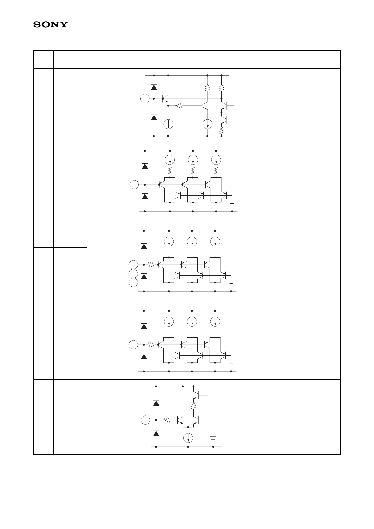
Pin Description
Pin
Symbol
Pin
Equivalent circuit Description
No. voltage
1
2
3
4
5
6
8
10
7
SDA
SCL
COFF-R
COFF-G
COFF-B
RIN
GIN
BIN
VCC2
—
—
—
—
5 V
1
VCC2
GND
4k
7.5k
7.5k
10k
5k
10k
15k
50µA
2
VCC2
GND
4k
10k
10k
5k
10k
15k
50µA
VCC2
GND
3
100
4
5
100
60k
50k
6
VCC2
GND
124
50µA
VCC1
8
10
5k
1mA
1k 1k
2k
2k
1k
I2C bus address and data input.
I2C bus clock signal input.
D/A converter outputs.
The variable range is 1 to 4 V.
Use as cut-off control voltages is
recommended.
R, G and B inputs.
When clamped, the input
voltage black level is
approximately 3.2 V.
Connect 0.1 µF or more in
series as a clamp capacitor.
5 V power supply.
Page 4
—4—
CXA2055P
Pin
Symbol
Pin
Equivalent circuit Description
No. voltage
9
11
12
13
14
15
16
SYNC
CON
CLP
OSDR
OSDG
OSDB
YS
BLK
—
—
—
—
VCC2
GND
10k
9
1k
24k 70k
50µA50µA
11
VCC1
GND
22µA
30k
1.3V
12
VCC1
GND
150µA
13
14
124
1.25V
15
VCC1
GND
150µA
124
1.25V
16
VCC1
GND
49k
124
1.5V
100µA
Sync signal separation circuit
block during sync-on-video
signal input. Connect a sampleand-hold capacitor.
Clamp pulse input. The polarity
can be switched via the I2C bus.
The threshold level is
approximately 1.3 V.
R, G and B OSD pulse inputs.
The threshold level is
approximately 1 V.
OSD-BLK pulse input.
The threshold level is
approximately 1.7 V.
BLK pulse input.
The threshold level is
approximately 1.5 V.
Page 5

—5—
CXA2055P
Pin
Symbol
Pin
Equivalent circuit Description
No. voltage
17
21
24
18
22
25
19
23
26
21
27
28
GND-B
GND-G
GND-R
B-OUT
G-OUT
R-OUT
B-S/H
G-S/H
R-S/H
VCC1
DA
/CSYNC
/ABL
VDET
/COF-RGB
0 V
—
—
12 V
—
VCC1
GND
200
18
22
25
VCC1
GND
19
23
26
1k
2.5V
1k1k1k
225µA
27
VCC2
GND
100
5k
50k
100k
100
4k
7.4k
1V
VCC2
GND
100
5k100
100
28
R, G and B independent GND.
R, G and B outputs.
Connection for external sampleand-hold capacitor (0.1 µF).
12 V power supply.
General-purpose D/A converter
output. Composite sync output.
TTL drive is possible.
VL=0.5 V or less, VH=4.0 V or more
RGB output amplitude gain
compensation input.
(common for all three channels)
Function switching is performed
via the I2C bus.
Video signal detection output.
VL=0.5 V or less, VH=4.0 V or more
General-purpose D/A converter
output.
The variable range is 1 to 4 V.
Function switching is performed
via the I2C bus.
Page 6

—6—
CXA2055P
Electrical Characteristics Measurement Circuit
SDA
SCL
COFF-R
COFF-G
COFF-B
RIN
V
CC2
GIN
SYNC CON
BIN
CLP
OSD-R
OSD-G
OSD-B
VDET/COFF-RGB
DA/CSYNC/ABL
R-S/H
R-OUT
GND-R
G-S/H
G-OUT
GND-G
V
CC1
B-S/H
B-OUT
GND-B
BLK
YS
0.1µ
5V
10µ
0.1µ
0.01µ
0.1µ
0.1µ
0.1µ
0.1µ
12V
10µ
Video detector output
DAC4 output
DAC1 output
DAC2 output
DAC3 output
75
75
75
0.1µ
S1
3
4
5
9
1
2
6
7
8
10
11
12
13
14
S2
Rch OUT
Gch OUT
0.1µ
Bch OUT
22
21
20
19
18
17
16
15
28
27
26
25
24
23
ABL input
I2C bus
control
Composite sync output
DAC5 output
Page 7

—7—
CXA2055P
Electrical Characteristics Measurement Circuit (For AC Measurement)
SDA
SCL
COFF-R
COFF-G
COFF-B
RIN
V
CC2
GIN
SYNC CON
BIN
CLP
OSD-R
OSD-G
OSD-B
VDET/COFF-RGB
DA/CSYNC/ABL
R-S/H
R-OUT
GND-R
G-S/H
G-OUT
GND-G
V
CC1
B-S/H
B-OUT
GND-B
BLK
YS
0.1µ
5V
10µ
12V
10µ
Video detector output
DAC4 output
DAC5 output
DAC1 output
DAC2 output
DAC3 output
50
0.1µ
Rch OUT
Gch OUT
0.1µ
Bch OUT
5k
50
5k
50
0.1µ
0.1µ
0.01µ
5k
3
4
5
9
1
2
6
7
8
10
11
12
13
14
22
21
20
19
18
17
16
15
28
27
26
25
24
23
I2C bus
control
Composite sync outpt
ABL input
Page 8

—8—
CXA2055P
Electrical Characteristics Ta=25 °C VCC1=12 V VCC2=5 V
No.
Measurement
Symbol Measurement contents Min. Typ. Max. Unit
item
1
2
3
4
Current
consumption
Frequency
response
Contrast
control
Subcontrast
gain
ICC1 (12 V)
ICC2 (5 V)
f 130 MHz
CONTMAX
SUBgain
S1 : GND, S2 : OFF
Input signal : none
Input continuous 1 MHz and 130 MHz sine
waves at 0.7 Vp-p.
Measure the output amplitude gain
difference at this time.
(
VOUT 130M
)
Gain difference [dB] =20log
V
OUT 1M
S1 : Pulse, S2 : OFF
Measure the output signal amplitude V
OUT
when a 0.7 Vp-p video signal is input.
Calculate the contrast gain from this V
OUT.
(
VOUT
)
CONTMAX [dB] =20log
0.7
S1 : Pulse, S2 : OFF
Measure the variable width of the output
signal amplitude V
OUT when a 0.7 Vp-p
video signal is input.
Gain difference [dB]=
CONTMAX [dB] –20log
(
VOUTSUBmin
)
0.7
— 82 115 mA
— 40 55 mA
— –3.0 — dB
16.0 16.5 — dB
10.5 13.5 — dB
GND
0.35V
0.7Vp-p
RGB input signal (RGB input pins)
CLP potential (approximately 3.2 V)
0.7Vp-p
RGB input signal
Either with or without
sync-on-green (sync signal)
SUBmax
SUBmin
RGB output signal
Either with or without
sync-on-green (sync signal)
Page 9

—9—
CXA2055P
No.
Measurement
Symbol Measurement contents Min. Typ. Max. Unit
item
5
6
7
8
9
Brightness
control
Input dynamic
range
Minimum
clamp pulse
width
OSD
control range
BLK control
BRTmax
BRTmin
Drang
CLPmin
OSDcont
BLKmax
BLKmin
S1 : Pulse, S2 : OFF
CLP pulse width: 350 ns
Measure the black level of the RGB output signal.
S1 : Pulse, S2 : OFF
Measure the level at which the output gain
can be secured when the input video signal
level is varied.
S1 : Pulse, S2 : OFF
Measure the clamp pulse width over which
the black level of the output signal V
OUT
does not change.
S1 : Pulse, S2 : OFF
Measure the variable width of the output
signal V
OUT when a 0.7 Vp-p video signal
is input.
(
OSDmax
)
Gain difference [dB] =20log
OSDmin
S1 : Pulse, S2 : OFF
Measure the BLK level of the output signal
when a 5.0 Vp-p BLK signal is input
3.4 3.7 —
V
— 0.5 0.7
0.9 1 1.2 Vp-p
200 — — nsec
4.0 5.0 — dB
1.7 1.9 —
V
— 0.1 0.4
GND
RGB output signal
Black level
Either with or without
sync-on-green (sync signal)
Video input
Pulse width
CLP pulse
OSDmax
OSDmin
RGB output signal
OSD interval
VBLK
GND
RGB output signal
Page 10

—10—
CXA2055P
P S Sr P
tLOW
tR
tHD;DAT tHIGH tSU;DAT tSU;STA tSU;STO
SDA
SCL
1
2
tBUF
tHD;STA
tF tHD;STA
(I2C BUS Logic System)
No.
1
2
3
4
5
6
7
8
9
10
11
12
13
14
Item
High level input voltage
Low level input voltage
Low level output voltage
SDA, during current inflow of 3 mA
Maximum clock frequency
Minimum waiting time for data change
Minimum waiting time for
data transfer start
Low level clock pulse width
High level clock pulse width
Minimum waiting time for
start preparation
Minimum data hold time
Minimum data preparation time
Rise time
Fall time
Minimum waiting time for stop
preparation
Symbol
VIH
VIL
VOL
fSCL
tBUF
tHD ; STA
tLOW
tHIGH
tSU ; STA
tHD ; DAT
tSU ; DAT
tR
tF
tSU ; STO
Min.
3.0
0
0
0
4.7
4.0
4.7
4.0
4.7
5
250
—
—
4.0
Typ.
—
—
—
—
—
—
—
—
—
—
—
—
—
—
Max.
5.0
1.5
0.4
100
—
—
—
—
—
—
—
1000
300
—
Unit
V
V
V
kHz
µs
µs
µs
µs
µs
µs
ns
ns
ns
µs
I2C BUS Control Signal
Page 11

—11—
CXA2055P
1. Application
The CXA2055P is a preamplifier for computer displays, and combines three R, G and B channels into a
single package. All controls such as the contrast and black level for each channel are performed via I2C
bus control.
1) I2C bus
Two wires (SDA, SCL) provide control over start, stop, data transfer, synchronization and collision
avoidance. The IC outputs are either open collector or open drain, forming a bus line in the wired OR
format. The bus signal configuration is as follows.
Data is transmitted by MSB-first. One data unit consists of 8 bits, to which the acknowledge signal,
which indicates that the data has been accepted by the slave, is attached at the end. Normally, the
slave ∗1IC receives data at the rising edge of SCL and the master ∗2IC changes data at the falling edge
of SCL. The actual data format is as follows.
SDA D A T A A D A T A
MSB LSB MSB LSB
SCL
S P
1 2 3 4 5 6 7 8 9 1 2 3 9
START STOP
S : Start condition; SDA is set at “low” when SCL is “high”.
P : Stop condition; SDA is set at “high” when SCL is “high”.
A : Acknowledge; Signal sent from the slave.
S A A A A A P
Slave address
40H
Subaddress
∗∗H
DATA0 DATA1 DATA2
Slave address configuration
BIT8 BIT7 BIT6 BIT5 BIT4 BIT3 BIT2 BIT1
Slave address R/W
The slave address is an address unique to each IC, and is assigned according to the IC functions. The
upper 7 of the 8 bits are the unique address and the final bit is the R/W bit. The R/W bit indicates read
∗3
when 1 and write ∗4when 0. 40H is allotted as the slave address for the CXA2055P. (This is write
only and there is no read mode.)
The subaddress is the assigned address within the IC, and is used for the various IC adjustments. The
subaddress is sent just once following the slave address, and is automatically incremented thereafter
until a stop condition is sent.
∗1
Slave : An IC that is placed under the control of the master.
In a normal system, all devices excluding the central microcomputer are slaves.
∗2 Master : A central microcomputer or other controlling IC.
∗3
Read : Mode where data is read from master to slave.
∗4
Write : Mode where data is written from master to slave.
Page 12

—12—
CXA2055P
2) Register map
• Slave address : 40H
• “∗” indicates undefined.
• Values inside parentheses ( ) are the initial setting values (during power-on reset)
(undetermined when not indicated)
Slave address configuration
BIT8 BIT7 BIT6 BIT5 BIT4 BIT3 BIT2 BIT1
0 1 0 0 0 0 0 R/W
SUB ADDRESS
00H
01H
02H
03H
04H
05H
06H
07H
08H
09H
0AH
0BH
0CH
0DH
0EH
BIT7 BIT6 BIT5 BIT4 BIT3 BIT2 BIT1 BIT0
CONTRAST
SUB CONTRAST R
SUB CONTRAST G
SUB CONTRAST B
∗ ∗ OSD GAIN BRT MODE (2)
BRIGHTNESS R (DA)
BRIGHTNESS G
BRIGHTNESS B
CUT OFF RGB
CUT OFF R
CUT OFF G
CUT OFF B
BLK (0)
∗ BLANKING LEVEL (0)
MODE
BRT SYNC VDET POWER
∗ CLP (0) VDET LEVEL
SW (0) POL (0) MODE (0) SAVE (0)
∗ ∗ ∗ ∗
D/A PINSW2 PINSW1 PINSW0
TEST (0) (0) (0) (0)
Page 13

—13—
CXA2055P
3) Description of registers (Numbers inside parentheses ( ) indicate the number of bits.)
CONTRAST (8) : Adjusts the R, G and B-OUT (Pins 25, 22 and 18) output amplitude gain
commonly for all three channels.
SUB CONTRAST (8) : Adjusts the R, G and B-OUT (Pins 25, 22 and 18) output amplitude gain
independently for each channel.
OSD GAIN (4) : Adjusts the OSD R, G and B (Pins 12, 13 and 14) OSD interval output signal
gain commonly for all three channels.
BRTMODE (2) : This register changes the output dynamic range.
The 2H setting is recommended.
0H : Output dynamic range 0.5 V to 4.5 V
1H : Output dynamic range 0.5 V to 5.5 V
2H : Output dynamic range 1.0 V to 6.5 V (recommended)
3H : Output dynamic range 2.0 V to 7.5 V
BRIGHTNESS (8) : Controls the output black level potential.
(Three-channel independent and common control can be selected by BRTSW.
During three-channel common mode, control is performed by the G channel.)
CUT OFF (8) : This is a general-purpose DAC. Use as a cut-off control is recommended.
BLK MODE (1) : Switches the blanking level mode
0H : BLK LEVEL=fixed
1H : BLK LEVEL=variable
BLANKING LEVEL (6) : Sets the blanking level when BLK MODE is set to 1H.
BRTSW (1) : Switches the brightness control between three-channel independent and
three-channel common control. When using three-channel common mode, the
BRIGHTNESS G channel is valid.
0H : Three-channel independent mode
1H : Three-channel common mode
SYNC POL (1) : Switches the sync separator output polarity during sync-on-green input.
0H : Positive polarity
1H : Negative polarity
VDET MODE (1) : Switches the video signal detection mode.
0H : B channel only is detected
1H : Signal obtained by adding R, G and B signals is detected
POWER SAVE (1) : Power save mode selector switch.
0H : Power save not performed
1H : Power save performed
Page 14

—14—
CXA2055P
CLP (1) : Selects the input clamp pulse polarity.
0H : Positive polarity input
1H : Negative polarity input
VDET LEVEL (2) : Threshold level selector switch for video interval detection. The threshold level
changes as follows.
(An input pulse width of as narrow as 10 ns can be detected.)
When VDET MOD=0H When VDET MOD=1H
0H : 300 mV or more 0H : Undetectable
1H : Undetectable 1H : Undetectable
2H : Undetectable 2H : 300 mV or more
3H : Undetectable 3H : 600 mV or more
Note) The threshold level when VDET MOD=1H is the total of the three
channel inputs.
D/A TEST (1) : DA TEST switch for IC measurement. Set to 0H.
PINSW : Switches the Pins 27 and 28 functions. (“∗” indicates don’t care.)
PINSW
2
0
1
0
1
∗
∗
1
0
0
1
1
0
1
0
0
0
0
0
1
1
Pin 28 output
DA (COFF_RGB)
DA (COFF_RGB)
VDET
VDET
DA (COFF_RGB)
VDET
Pin 27 output
C-SYNC
ABL (CONTRAST)
C-SYNC
ABL (CONTRAST)
DA (BRIGHTNESS)
DA (BRIGHTNESS)
Note) When the Pin 27 output is set to DA (BRIGHTNESS),
BRIGHTNESS is forcibly set to the three-channel common
mode.
Page 15

—15—
CXA2055P
2. Blanking addition function
The output is blanked while the BLK pin (Pin 16) is high level.
The BLK pin threshold level is approximately 1.5 V.
3. OSD addition function and OSD contrast control
OSD can be added to the video signal while the OSD-R, G and B pins (Pins 12, 13 and 14) are high level.
OSD blanking is added when any of these three channels is high level.
OSD blanking is also added to all three channels while the YS pin (Pin 15) is high level. See the following
logic.
4. CONTRAST function
The CONTRAST function performs gain control for the R, G and B-OUT output amplitudes.
5. ABL function
ABL control can be performed by Pin 27 by setting PINSW. The variable range is approximately 13.7 dB.
See the characteristics diagrams hereafter for the control characteristics.
YS PULSE
from 15pin
OSD PULSE (R)
from 12pin
OSD PULSE (G)
from 13pin
OSD PULSE (B)
from 14pin
Ys Circuit (R, G, B)
1 : Active
0 : Passive
OSD Circuit (R)
1 : Active
0 : Passive
OSD Circuit (G)
1 : Active
0 : Passive
OSD Circuit (B)
1 : Active
0 : Passive
Page 16

—16—
CXA2055P
I/O Signal Example
0.7Vp-p (typ)
Video In
GND
Clp Pulse
Blanking Pulse
Ys Pulse
OSD Pulse
Video Out
C-Sync Out
Vdet Out
tCLP ≥ 200nsec
Clamp DC voltage
Approximately 3.2 V
Page 17

—17—
CXA2055P
Application Circuit
VDET/COFF-RGB
DA/CSYNC/ABL
R-S/H
R-OUT
GND-R
G-S/H
G-OUT
GND-G
V
CC1
B-S/H
B-OUT
GND-B
BLK
YS
0.1µ
0.1µ
5V
10µ
75Ω
75Ω
0.1µ
75Ω
0.1µ
0.1µ
Rch video input
Gch video input
Bch video input
Clamp pulse input
Rch OSD input
Gch OSD input
Bch OSD input
0.1µ
Rch
DISPLAY POWER AMP
Rch
to CRT
cathode
Gch
to CRT
cathode
0.1µ
12V
10µ
Gch
DISPLAY POWER AMP
Bch
to CRT
cathode
Video detector output
DAC4 output
DAC1 output
DAC2 output
DAC3 output
BLANKING pulse input
YS input
0.1µ
0.1µ
22
21
20
18
17
16
15
28
27
26
25
24
23
19
Bch
DISPLAY POWER AMP
3
4
5
9
1
2
6
7
8
10
11
12
13
14
SDA
SCL
COFF-R
COFF-G
COFF-B
RIN
V
CC2
GIN
SYNC CON
BIN
CLP
OSD-R
OSD-G
OSD-B
I2C bus
control
Composite sync output
ABL input (0V to 4V)
DAC5 output
Application circuits shown are typical examples illustrating the operation of the devices. Sony cannot assume responsibility for
any problems arising out of the use of these circuits or for any infringement of third party patent and other right due to same.
Page 18

—18—
CXA2055P
Notes on Board Pattern and Layout
1. When not using the OSD, YS or BLK pins, connect these pins to GND.
2. Care should be taken for the following items regarding the output signals from R, G and BOUT.
1) Connect these signal lines so that they are high impedance to external circuits.
2) Do not allow current to flow into the IC side.
3) Arrange the signal lines so that the distance to the power amplifier is as short as possible.
3. The VCC1 and VCC2 decoupling capacitors should consist of ceramic capacitors and electrolytic capacitors
connected in parallel, and should be connected as close to the IC as possible.
4. The R, G and BIN clamp capacitors should be located as close to the IC as possible.
5. The sample-and-hold capacitors connected to the R, G and B-S/H pins should be connected as close to the
IC as possible.
6. The output signals from COFF-R, G and B should be arranged so that capacitance of 20 pF or more is not
applied to the pins or the pattern.
Page 19

—19—
CXA2055P
0 32 64 96 128 160 192 224
0
500
1000
1500
2000
2500
3000
3500
4000
4500
5000
mVp-p
Subcontrast Control=FFH
Subcontrast Control=7FH
Subcontrast Control=00H
BUS DATA
0 1 2 3 4 5
0
500
1000
1500
2000
2500
3000
3500
4000
4500
5000
mVp-p
V
0 32 64 96 128 160 192 224
0.000
0.500
1.000
1.500
2.000
2.500
3.000
3.500
4.000
V
BUS DATA
0 8 24 32 40
0
200
400
600
800
1000
1200
1400
1600
1800
2000
mV
BUS DATA
16 48 56
0 2 4 6 8 10 12 14
mVp-p
BUS DATA
0
500
1000
1500
2000
2500
3000
3500
4000
4500
5000
5500
6000
Subcontrast Control=FFH
Subcontrast Control=7FH
Subcontrast Control=00H
Contrast control characteristics, subcontrast control characteristics
Input amplitude 700mVp-p
Output amplitude
ABL characteristics
Output amplitude
Control voltage
Brightness control characteristics
Output black level
BLK control characteristics
Output BLK level
OSD control characteristics
OSD interval output amplitude
Page 20

0.25 – 0.05
+ 0.1
Package Outline Unit : mm
28 15
1 14
+ 0.4
37.8 – 0.1
28PIN DIP (PLASTIC)
15.24
2.54
CXA2055P
0° to 15°
+ 0.3
13.0 – 0.1
Two kinds of package surface:
1.All mat surface type.
2.Center part is mirror surface.
SONY CODE
EIAJ CODE
JEDEC CODE
0.5 ± 0.1
1.2 ± 0.15
DIP-28P-03
DIP028-P-0600
+ 0.4
4.6 – 0.1
0.5 MIN
3.0 MIN
PACKAGE STRUCTURE
PACKAGE MATERIAL
LEAD TREATMENT
LEAD MATERIAL
PACKAGE MASS
EPOXY RESIN
SOLDER PLATING
COPPER ALLOY
4.2g
—20—
 Loading...