

Page 1

Electronic Volume
For the availability of this product, please contact the sales office.
Description
The CXA2506Q is a 2-channel electronic volume
IC. A 34-bit serial data input controls the level and
characteristics of the output signal. It may be used
in car stereos and general audio systems.
Features
• Loudness (Full boost at –32 dB or less of VRC)
• Volume control
(from 0 dB to –87 dB, –∞ dB: Fine (1 dB-step)
Coarse (8 dB-step)
• Balance
• Tone control
(3-band, 2 dB-step from –15 dB to +15 dB)
• Fader
(2 dB-step to –20 dB, –25 dB, –35 dB, –45 dB, –60
dB, –∞ dB)
• Input and gain selector (4 channels)
• Serial data control (DATA, CLK, CE)
• Single 8 V power supply
• Zero-cross detection circuit
• Timer
• Power-off mute
CXA2506Q
48 pin QFP (Plastic)
Absolute Maximum Ratings (Ta=25 °C)
• Supply voltage VCC 13 V
• Operating temperature Topr –40 to +85 °C
• Storage temperature Tstg –65 to +150 °C
• Allowable power dissipation
PD 350 mW
(Ta = 85 °C)
Recommended Operating Condition
• Supply voltage VCC 6 to 12 V
Structure
Bipolar IC
Sony reserves the right to change products and specifications without prior notice. This information does not convey any license by
any implication or otherwise under any patents or other right. Application circuits shown, if any, are typical examples illustrating the
operation of the devices. Sony cannot assume responsibility for any problems arising out of the use of these circuits.
—1—
E96X02B7Y
Page 2

Block Diagram and Pin Configuration
LDHC1
LDLC1
GAIN134
CXA2506Q
FDIN1
TCO1
TCLC12
TCLC11
TCMC12
TCMC11
TCHC1
VRI N1
INAO1
252627282930313233343536
GAIN12
GAIN11
IN14
IN13
IN12
IN11
IN21
IN22
IN23
IN24
GAIN21
GAIN22
37
38
39
40
41
42
43
44
45
46
47
48
INPUT SWITCH
INPUT SWITCH
LOUD
LOUD
ZCDET
8dB STEP
VOLUME
VOLUME
8dB STEP
1dB STEP
VOLUME
LA TC H
SHIFT R EGI STER
VOLUME
1dB STEP
1 2 3 4 5 6 7 8 9
TONE FADER
VCTBUFF
VCTBUFF
VCTBUFF
VCTBUFF
VCTBUFF
VCTBUFF
LA TC H
CONTROL
TONE FA DER
10 11 12
24
23
22
21
20
19
18
17
16
15
14
13
FNTO1
REO1
CE
CLK
DGND
GND
VCC
VCT
DATA
TIMER
REO2
FNTO2
DLC2
GAIN234
LDHC2
VRI N2
INAO2
TCHC2
TCLC21
TCMC22
TCMC21
TCO2
TCLC22
FDIN2
—2—
Page 3

Pin Description and Equivalent Circuit
CXA2506Q
Pin
No. Pin voltage
35
34
2
3
Pin Name
LDLC2
LDLC1
LDHC2
LDHC1
I/O Resistance
6.18 k
VCT
8.92 k
VCT
35
34
Equivalent Circuit Description
V
CC
2
Sets loudness low cut-off
frequency.
GND
V
CC
3
Set loudness high cut-off
frequency
GND
4
33
5
32
INAO2
INAO1
VRIN2
VRIN1
—
VCT
10 k
VCT
33
32
V
CC
4
GND
V
CC
5
GND
V
CC
Input selector output
Volume input
6
31
TCHC2
TCHC1
5 k
VCT
31
6
GND
Set tone Treble frequency
—3—
Page 4

CXA2506Q
Pin
No. Pin voltage
30
29
7
8
Pin Name
TCMC21
TCMC11
TCMC22
TCMC12
I/O Resistance
4 k
VCT
4 k
VCT
30
29
Equivalent Circuit Description
V
CC
7
GND
V
CC
8
GND
Sets tone Mid frequency
Sets tone Mid frequency
28
10
27
9
TCLC21
TCLC11
TCLC22
TCLC12
8 k
VCT
8 k
VCT
28
10
27
V
CC
9
GND
V
CC
Sets tone Bass frequency
Sets tone Bass frequency
GND
V
CC
11
26
TCO2
TCO1
—
VCT
11
26
Tone control output
GND
—4—
Page 5

CXA2506Q
Pin
No. Pin voltage
12
25
13
24
Pin Name
FDIN2
FDIN1
REO2
REO1
I/O Resistance
24 k
VCT
—
VCT
12
25
13
24
Equivalent Circuit Description
V
CC
Fader input
GND
V
CC
Rear output
GND
14
23
15
FNT02
FNT01
TIMER
—
VCT
~ ∞
—
14
23
15
V
CC
GND
V
CC
GND
CC
V
Front output
Sets timer constant
16
DATA
~ ∞
—
16
Serial data input
GND
—5—
Page 6

CXA2506Q
Pin
No. Pin voltage
17
18
19
20
21
Pin Name
VCT
VCC
GND
DGND
CLK
I/O Resistance
—
VCT
—
VCC
—
Gnd
—
—
~ ∞
—
21
Equivalent Circuit Description
1/2 VCC
Power supply input
Ground
Digital ground
V
CC
Serial clock input
GND
22
1
36
37
38
47
49
39
40
41
42
43
44
45
46
CE
GAIN234
GAIN134
GAIN12
GAIN11
GAIN21
GAIN22
IN14
IN13
IN12
IN11
IN21
IN22
IN23
IN24
~ ∞
—
~ ∞
VCT
50 k
VCT
22
1
36
37
38
47
48
39 40
41 42
43 44
45 46
CC
V
GND
CC
V
GND
V
GND
Latch enable input
External gain setting for input
amplifier
CC
Signal input
—6—
Page 7
Data Format
CXA2506Q
First Bit
Last Bit
D1 NOP
D2 NOP
D3
D4
ISW
D5 LOUD
D6
D7
D8
VRC1
D9
D10
D11 VRF1
D12
D13
D14
D15
VRC2
D16
D17
D18 VRF2
D19
D20
D21
D22
TONE BASS
D23
D24
D25
D26
TONE MID
D27
D28
D29
D30
TONE TREBLE
D31
D32
D33
D34
FADER
D35
D36 FADER SELECT
—7—
Page 8
ISW
MODE D3 D4
IN14/IN24, GAIN134/GAIN234
IN13/IN23, GAIN134/GAIN234
IN12/IN22, GAIN12/GAIN22
IN11/IN21, GAIN11/GAIN21
1
1
0
0
LOUD
MODE D5
ON 1
OFF 0
VRC1/VRC2
OUTPUT (dB) D6/D13 D7/D14 D8/D15 D9/D16
0
–8
–16
–24
–32
–40
–48
–56
–64
–72
–80
– ∞
– ∞
1
1
1
1
1
1
1
1
0
0
0
0
0
1
1
1
1
0
0
0
0
1
1
1
1
0
1
1
0
0
1
1
0
0
1
1
0
0
0
CXA2506Q
1
0
1
0
1
0
1
0
1
0
1
0
1
0
1
0
0
—8—
Page 9
VRF1/VRF2
OUTPUT (dB) D10/D17 D11/D18 D12/D19
–1
–2
–3
–4
–5
–6
–7
0
1
1
1
1
0
0
0
0
1
1
0
0
1
1
0
0
BASS/MID/TREBLE
OUTPUT (dB) D20/D24/D28 D21/D25/D29 D22/D26/D30
15
12
10
1
1
1
8
6
4
2
0
1
0
0
0
0
1
1
0
0
1
1
0
0
CXA2506Q
1
0
1
0
1
0
1
0
1
0
1
0
1
0
1
0
BOOST/CUT
MODE D23/D27/D31
BOOST 1
CUT 0
—9—
Page 10
FADER
OUTPUT (dB) D32 D33 D34 D35
– ∞
–60
–45
–35
–25
–20
–18
–16
–14
–12
–10
–8
–6
–4
–2
0
1
1
1
1
1
1
1
1
0
0
0
0
0
0
0
0
1
1
1
1
0
0
0
0
1
1
1
1
0
0
0
0
1
1
0
0
1
1
0
0
1
1
0
0
1
1
0
0
CXA2506Q
1
0
1
0
1
0
1
0
1
0
1
0
1
0
1
0
FADER SELECT
MODE D36
FRONT 1
REAR 0
RESET
Reset is performed automatically when power is first supplied to the IC; there is no reset pin.
The following table shows the respective statuses of various settings after a reset has been performed.
However, from the time when power is first supplied until the first data transfer, keep CE high by pulling it up to
VCC, etc.
MODE SET VALUE
INPUT 1
VRC1 – ∞ dB
VRF1 –7 dB
VRC2 – ∞ dB
VRF2 –7 dB
LOUD OFF
TONE BASS 0 dB
TONE MID 0 dB
TONE TREBLE 0 dB
FADER 0 dB, REAR
—10—
Page 11
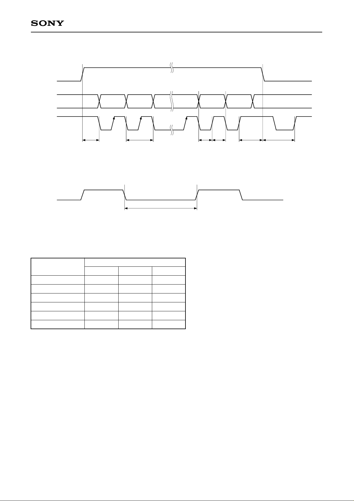
Timing Chart
CE
CXA2506Q
DATA
CLK
CE
t1 tck tsu th t2 tL
t
1 ≥ 0.5µs
t2 ≥ 0.5µs
tck ≥ 1.0µs
tsu ≥ 0.5µs
th ≥ 0.5µs
tce ≥ 4.0µs
D1 D2 D34 D35 D36 Invalid
t
L ≥ tT+0.5µs
(tT is the maximum value for the timer operation time)
tce
Timer Waiting Period Setting Chart (VCC = 6 to 12 V, operating temperature=–40 °C to 85 °C)
TIMER pin
capacitance C
C = 100 pF
C = 0.001 µF
C = 0.01 µF
C = 0.1 µF
C = 1 µF
C = 10 µF
Min. Typ. Max.
3 µs 5 µs 9 µs
30 µs 50 µs 90 µs
300 µs 500 µs 900 µs
3 ms 5 ms 9 ms
30 ms 50 ms 90 ms
300 ms 500 ms 900 ms
Waiting period
—11—
Page 12

Electrical Characteristics
Item Symbol Conditions Min. Typ. Max Unit
Current consumption
Total Harmonic distortion
Output noise voltage
Max output voltage
Separation
Max. attenuation factor
Loudness LOW
Loudness HIGH
Bass max. boost gain
Bass max. cut gain
Mid max. boost gain
Mid max. cut gain
Treble max. boost gain
Treble max. cut gain
Input voltage HIGH
Input voltage LOW
Input voltage range
ICC
THD
Vn
Vom
CS
ATTm
Glb
Glh
Gbb
Gbc
Gmb
Gmc
Gtb
Gtc
Vsh
Vsl
Vin
VCC=8 V, Ta=25 °C, Input=0 dB unless otherwise specified
No signal
1 kHz, 5 dBm output
Short-circuit at input, A weight
1 kHz
1 kHz
100 Hz, VRC=–16 dB
10 kHz, VRC=–16 dB
DATA, CLK, CE
DATA, CLK, CE
IN11 to 14
IN21 to 24
VRIN1, 2
FDIN1, 2
CXA2506Q
—2128mA
— 0.003 0.01 %
— 8 10 µVrms
8 — — dBm
72 90 —
85 90 —
789
567
13 15 17
13 15 17
dB
13 15 17
13 15 17
13 15 17
13 15 17
3—6
0 — 1.5
1—VCC–1
V
—12—
Page 13
5V
0V
5V
0V
5V
CXA2506Q
0V
V4
C6
AC
C15
0.39µ
C18
C14
B
A
10µ
B
A
S1
0.022µ
0.033µ
0.0027µ
C8
S2
820p
0.15µ
10k
10µ
10µ
C12
C10
10k
10k
C4
C2
R5
10k
R4
R2
1k
C21
1k
R15
10k
FDIN1
TCO1
VRIN1
INAO1
LDHC1
LDLC1
GAIN12
10k
R12
TCLC12
TCLC11
TCMC12
TCMC11
TCHC1
GAIN134
38
220p
1k
R19
R15
10k
23
REO1
GAIN11
R20
OPAMP
R18
10k
R17
R13
FNTO1
24
S5_A
25
26
27
28
29
30
31
32
33
34
35
36
37
CE
CLK
AC
V5
-60dBm
3-6V
V3
V2
1k
1k
R10
R11
21
22
CE
IN14
39
S14
A
B
B
V14
AC
20
CLK
DGND
IN12
IN13
40
41
S13
S12
A
B
A
V13
AC
B
V12
AC
V
CC
100µ
C19
19
18
CC
V
GND
IN21
IN11
42
43
S21
S11
A
B
A
V11
AC
S4
B
V21
AC
3-6V
VEE
S22
DATA
C20
V1
0.01µ
1k
R9
16
17
VCT
DATA
IN23
IN22
44
45
S23
A
B
A
V22
AC
B
V23
AC
10k
R14
A
B
R8
V24
AC
R7
10k
10k
14
REO2
GAIN21
47
FNTO2
13
48
FDIN2
TCO2
TCLC22
TCLC21
TCMC22
TCMC21
TCHC2
VRIN2
INAO2
LDHC2
LDLC2
GAIN234
GAIN22
S5_B
B
V6
10µ
10µ
AC
A
C17
0.39µ
C15
C13
0.022µ
C11
0.033µ
C9
0.0027µ
C7
12
11
10
9
8
7
6
5
C5
10µ
4
820p
3
C3
0.15µ
2
C1
10k
1
R5
10k
R3
10k
R1
S3
15
TIMER
IN24
46
S24
A
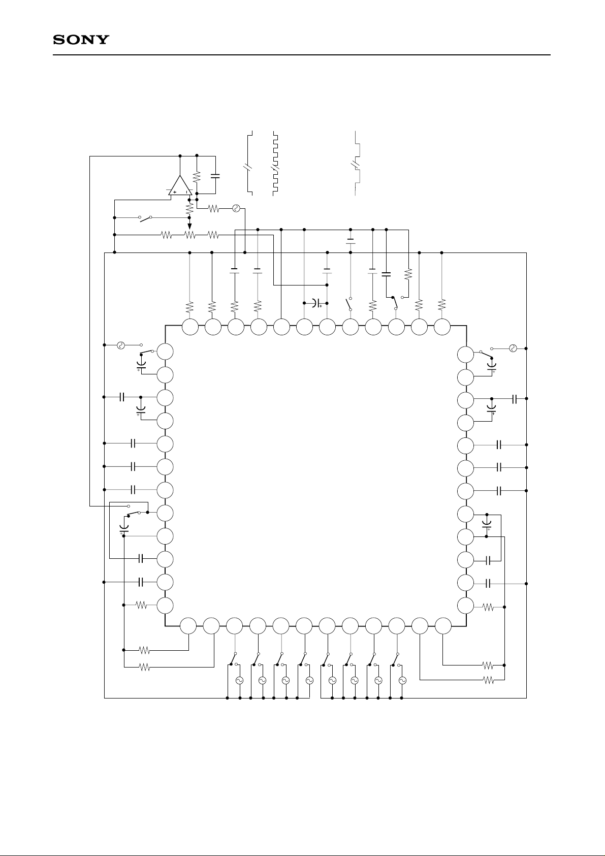
Electrical Characteristic Test Circuit
—13—
Page 14
CXA2506Q
C6
20
DGND
IN12
41
TO POWER SUPPLY
10µ
C21
33µ
C19
19
18
CC
V
GND
IN21
IN11
43
42
R9
17
VCT
IN22
44
C20
1k
R8
0.01µ
15
16
DATA
TIMER
IN24
IN23
45
46
14
REO2
47
GAIN21
10k
R7
10k
FNTO2
13
FDIN2
12
10µ
10µ
10k
10µ
C11
C9
C7
C3
C1
10k
R5
10k
C17
C13
C5
820p
0.15µ
R3
R1
0.022µ
0.033µ
0.0027µ
0.39µ
C15
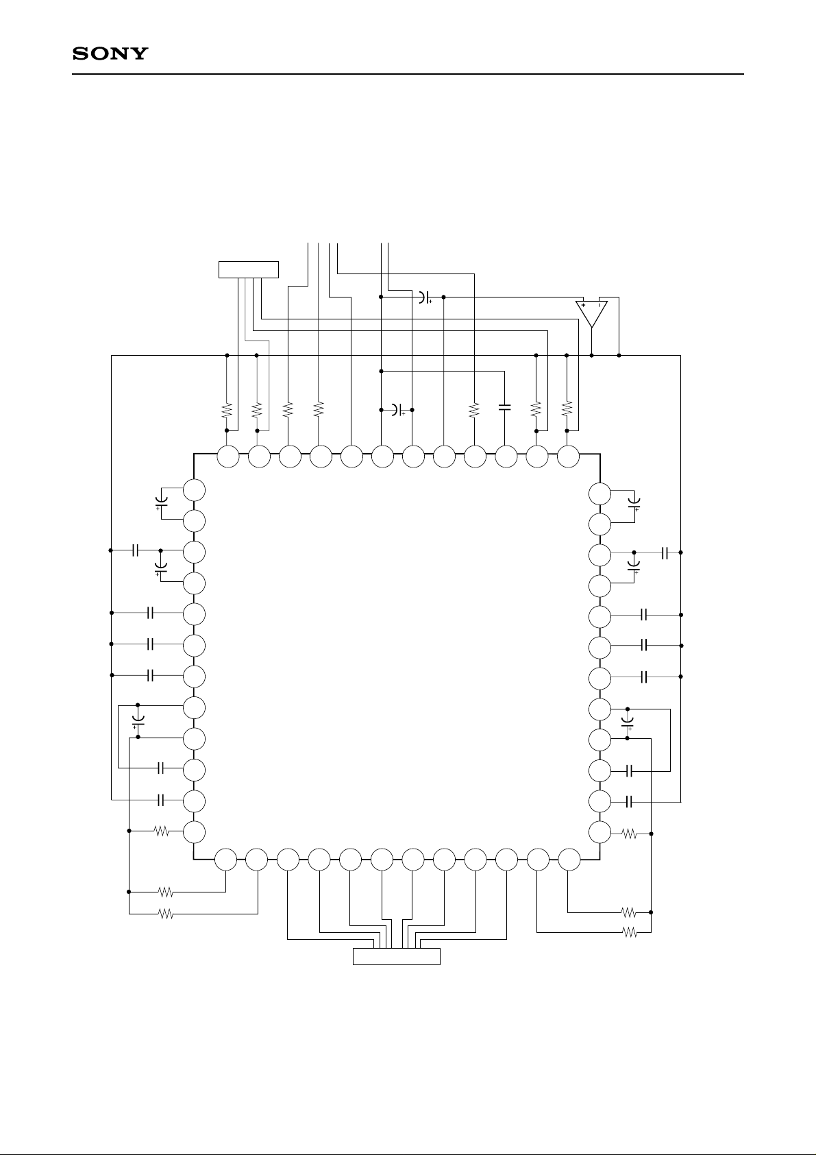
Application circuits shown are typical examples illustrating the operation of the devices. Sony cannot assume responsibility for
any problems arising out of the use of these circuits or for any infringement of third party patent and other right due to same.
TCO2
11
TCLC22
10
TCLC21
9
TCMC22
8
TCMC21
7
TCHC2
6
VRIN2
5
INAO2
4
LDHC2
3
LDLC2
2
GAIN234
1
48
GAIN22
TO CP U
OUTPUT SIGNAL
10k
1k
39
22
CE
IN14
1k
R10
21
CLK
IN13
40
10k
R11
R12
R13
FNTO1
24
23
25
10µ
C18
10µ
R5
0.022µ
0.033µ
0.0027µ
820p
10k
C8
0.15µ
10k
10k
10µ
C12
C10
26
27
28
29
30
31
32
33
34
35
36
R4
R2
0.39µ
C15
C14
C4
C2
FDIN1
REO1
TCO1
TCLC12
TCLC11
TCMC12
TCMC11
TCHC1
VRIN1
INAO1
LDHC1
LDLC1
GAIN134
GAIN11
38
37
GAIN12
Application Circuit
SOURCES
INPUT SIGNAL
—14—
Page 15
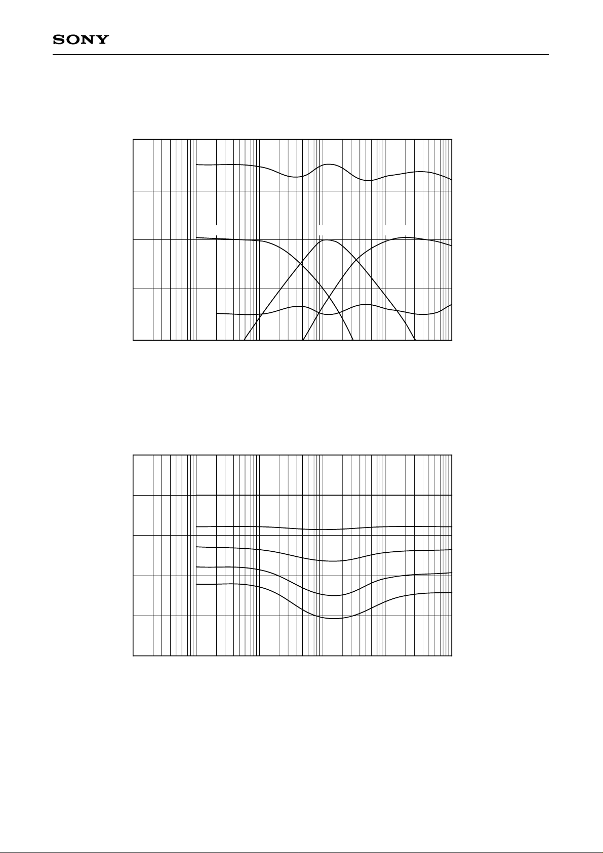
Example if Representative Characteristics
Tone Control Frequency Characteristics
20
CXA2506Q
10
BASS MID TREBLE
0
Voltage (dB)
–10
–20
1 10 100 1k 10k 100k
Frequency (Hz)
Loudness Frequency Characteristics
10
15dB
–15dB
0
–10
–20
Voltage (dB)
–30
–40
1 10 100 1k 10k 100k
Frequency (Hz)
VRC=0dB
VRC=–8dB
VRC=–16dB
VRC=–24dB
VRC=–32dB
—15—
Page 16
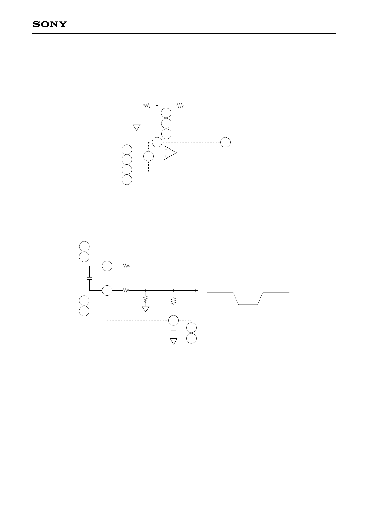
Description of Operation
(1) Gain of input amplifier
The input selector stage may be configured as a buffer or a non-inverting amplifier.
CXA2506Q
2/R1
GAIN134
GAIN12
GAIN11
CXA2506Q
Input amp of channel 1
33
INA01
39
40
41
42
R1 R2
VCT
IN14
IN13
IN12
IN11
Gain=1+R
36
37
38
(2) Loud
The loudness function achieves the necessary frequency characteristics by using a filter as shown below.
The resistors are built in so that fL and fH can be set by selecting C1 and C2.
34
3
LDHC1
LDHC2
R2=21.93k
fL=1/(2πC1R1)
fH=1/(2πC2R2)
32
5
C2
VRIN1
VRIN2
30k
3.79k
CXA2506Q
VCT
VCT
R1=1.84k
C1
35
2
fH
fL
LDLC1
LDLC2
—16—
Page 17
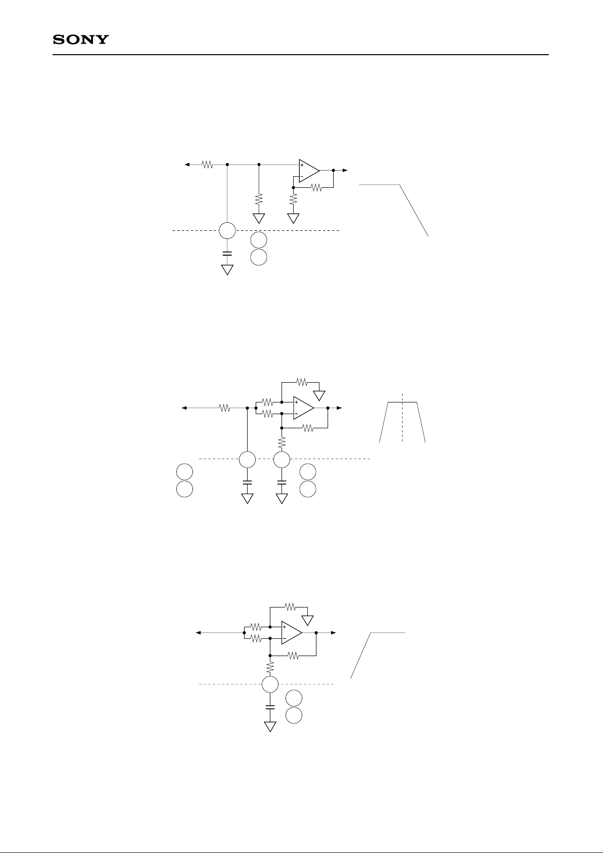
(3) Tone control
BASS: LPF
CXA2506Q
fL=1/(2πC1R1//R2)
R1=8k
MID: BPF
R2=8k 8k
VCT
VCT VCT
27
TCLC12
18
TCLC22
fL=1/(2πC2R3)
fH=1/(2πC3R4)
HPF
4k
4k
R4=8k
C3
16k
CXA2506Q
C1
LPF
R3=4k
29 38
TCMC12
TCMC22
C2
8k
16k
78
VCT
CXA2506Q
TCMC11
TCMC21
fL
fH fL
fM
TREBLE: HPF
CXA2506Q
VCT
10k
10k
R5=5k
VCT
fH=1/(2πC4R5)
C4
VCT
10k
10k
31
6
VCT
TCHC11
TCHC21
fH
—17—
Page 18
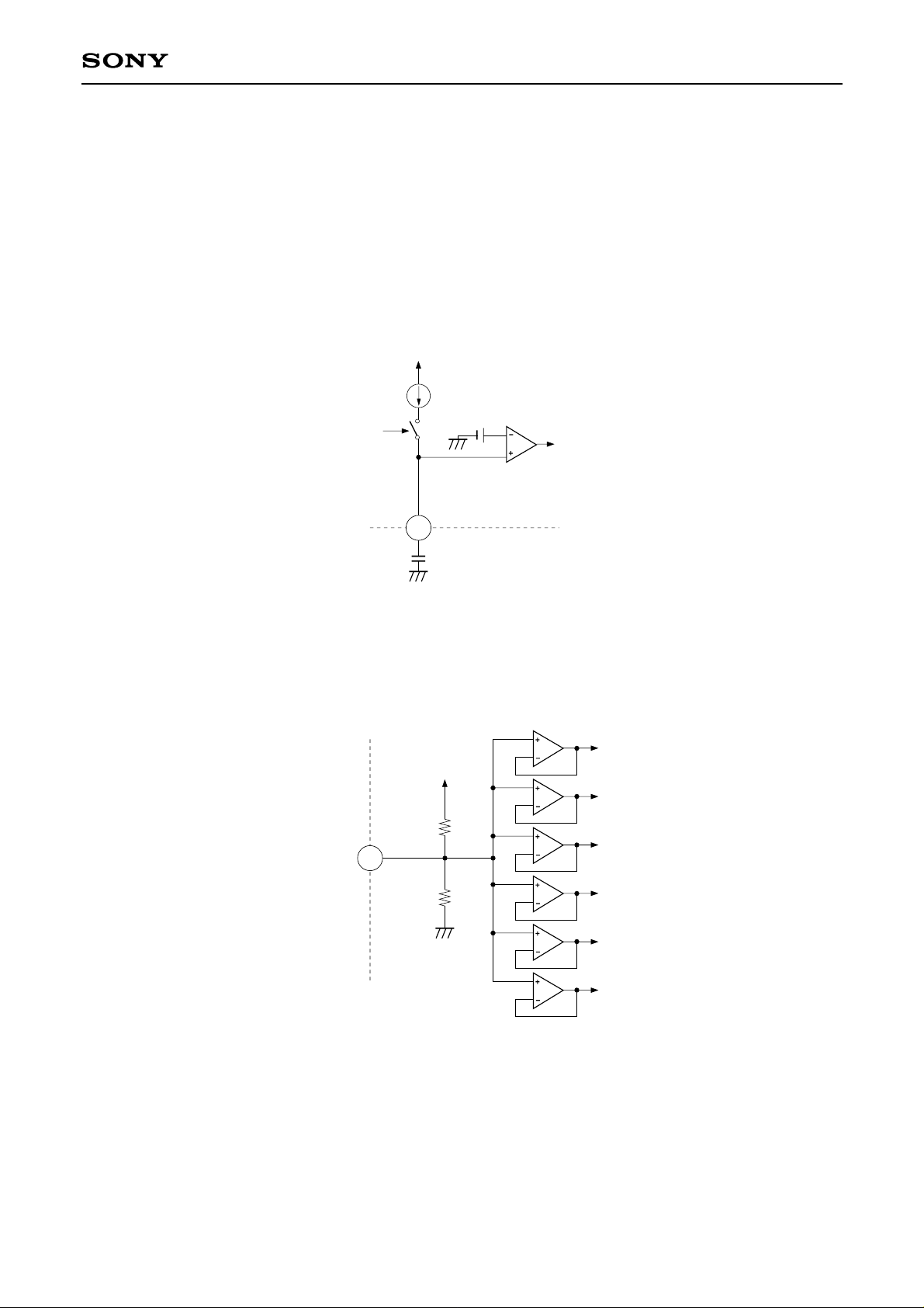
(4) Zero-cross detector and Timer
A built-in zero-cross detection circuit is used to detect the zero-cross points of the input signal. When data
arrived at the IC, they are executed at the next zero-cross point or when there is no input signal. This is to
minimize 'click' noise during the transition of levels.
The timer circuit is added to ensure that the data is executed even when a zero-cross point is not detected
after a pre-determined period of time from the falling edge of the CE pulse.
Time constant=(0.5/10µ) × C [sec]
VCC
10µA
CXA2506Q
CE
15
0.5V
CXA2506Q
TIMER
C
(5) VCT pin
The internal circuit of VCT pin has the following structure.
Insert a buffer when using it as a reference voltage for an external circuit.
VCC
100k
VCT
17
CXA2506Q
100k
GND
(6) Power-off Mute
This function mutes the output pins FNTO1, FNTO2, REO1 and REO2, when the VCC goes below 5V, by
turning off the bias of the output stage of the fader circuit. By so doing, the 'pop' noise caused by the drop
in these pins potential from VCC/2 during power-off can be avoided.
—18—
Page 19

Package Outline Unit : mm
CXA2506Q
48PIN QFP (PLASTIC)
15.3 ± 0.4
+ 0.4
12.0 – 0.1
2536
37
48
112
0.8 0.3 – 0.1
+ 0.15
24
13
± 0.12
M
+ 0.35
2.2 – 0.15
+ 0.1
0.15 – 0.05
0.15
+ 0.2
0.1 – 0.1
13.5
0.9 ± 0.2
PACKAGE STRUCTURE
EPOXY RESIN
SOLDER / PALLADIUM
PLATING
COPPER / 42 ALLOY
0.7g
SONY CODE
EIAJ CODE
JEDEC CODE
QFP-48P-L04
∗QFP048-P-1212-B
PACKAGE MATERIAL
LEAD TREATMENT
LEAD MATERIAL
PACKAGE WEIGHT
NOTE : PALLADIUM PLATING
This product uses S-PdPPF (Sony Spec.-Palladium Pre-Plated Lead Frame).
—19—
 Loading...