

Page 1

– 1 –
CXA2039M
24 pin SOP (Plastic)
E96X26C1Y-PS
Base Band Hue/Color Control
Description
The CXA2039M is a bipolar color difference signal
processing IC for color TVs. This chip enables base
band hue and color control for color difference
signals.
Features
• 2 UV inputs, 1 UV output
• 3 Y inputs, 2 Y outputs
(1 of the 2 outputs outputs either of 2 inputs.)
• Built-in color difference signal delay line circuit
Absolute Maximum Ratings
• Supply voltage VCC 12 V
• Operating temperature Topr –20 to +75 °C
• Storage temperature Tstg –65 to +150 °C
• Allowable power dissipation
P
D 780 mW
Operating Conditions
Supply voltage V
CC 9 ± 0.5 V
Applications
Color TVs
Structure
Bipolar silicon monolithic IC
Sony reserves the right to change products and specifications without prior notice. This information does not convey any license by
any implication or otherwise under any patents or other right. Application circuits shown, if any, are typical examples illustrating the
operation of the devices. Sony cannot assume responsibility for any problems arising out of the use of these circuits.
Page 2

– 2 –
CXA2039M
CLAMP
Delay
Line
CLAMP
DRIVE
ATT
ATT
Y
ATT
ATT
YUV SW
R-Y
B-Y
ATT
HUE
COLOR
LEVEL
IREFCLAMP
13
14
15
16
17
18
19
20
21
22
23
24
11
12
2
3
4
5
6
7
8
9
10
1
V
CC
Y2 IN
RY2 IN
BY2 IN
GND
TV IN
Y SW
HUE
COLOR
DLY
GND
DLY SW
Y1 IN
RY1 IN
BY1 IN
GND
CLAMP
YUV SW
LEVEL
Y OUT
RY OUT
BY OUT
V
CC
TV OUT
Y2
R-Y2
B-Y2
Delay SW
Y SW
TV
Y1
R-Y1
B-Y1
Block Diagram
Page 3

– 3 –
CXA2039M
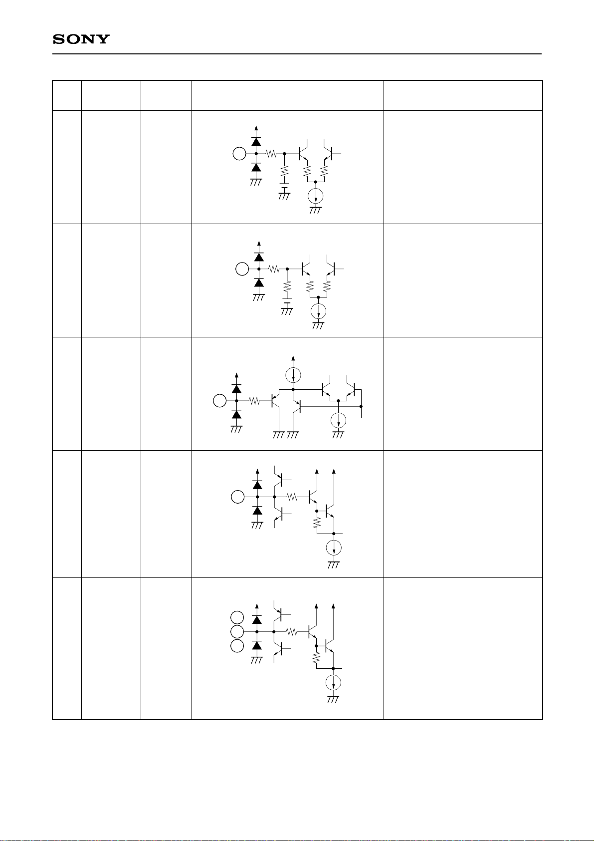
Pin Description
Pin
No.
Symbol Pin voltage Equivalent circuit Description
1
2
3
Y1 IN
RY1 IN
BY1 IN
Y1, R-Y1 and B-Y1 signal inputs.
Input the signals via capacitors.
4
1420GND
GND.
6 YUV SW
YUV SW control.
YUV SW ≤ 0.4V →
Y2 IN, RY2 IN,
and BY2 IN
signals
selected.
YUV SW ≥ 1.0V →
Y1 IN, RY1 IN,
and BY1 IN
signals
selected.
VCC
1.5k
VCC
60k
6
5 CLAMP
Clamp pulse (positive polarity)
input.
VILMAX = 2.5V
VIHMIN = 3.5V
VCC
8k
5
VCC
20p
7 LEVEL
RY OUT, BY OUT and TV OUT
output level control.
VILMAX = 6.0V
VIHMIN = 6.8V
7
VCC
56k
36k
8 Y OUT
Y signal output.
Outputs the signals input to Pins 1
and 23 attenuated by –6dB.
VCC
VCCVCC
20k
4k
8
2
3
1
VCC VCC VCC
70k
1.5k
Page 4

– 4 –
CXA2039M
9 RY OUT R-Y signal output.
VCC
VCCVCC
30k
4k
9
10 BY OUT B-Y signal output.
VCC
VCCVCC
30k
4k
10
12 TV OUT Y signal output.
VCC
VCC
30k
3k
1k
12
13 DLY SW
Delay on/off switching signal
input.
DLY SW ≤ 1.4V → Delay off
DLY SW ≥ 2.2V → Delay on
13
60k
VCC
15 DLY
Delay line reference current
setting. Connect to GND via a
resistor. When 10kΩ is
connected, the delay time is
600ns. Increasing the resistance
value increases the delay time
and vice versa.
VCC
40k
15
18k
11
24
VCC 9V Power supply.
Pin
No.
Symbol Pin voltage Equivalent circuit Description
Page 5
– 5 –
CXA2039M
16 COLOR
Color control.
Control is performed by applying
a voltage of 0 to 9V.
VCC
8k
60k
8k20k
4.5V
16
18 Y SW
Y SW control.
DLY SW ≤ 1.4V → TV IN signal
selected.
DLY SW ≥ 2.2V → Y1 IN or Y2
IN signal
selected
(selected by
YUV SW).
VCC
18
VCC
1.5k
19 TV IN
Y signal input.
Input the signal via a capacitor.
VCC VCC VCC
70k
1.5k
19
21
22
23
BY2 IN
RY2 IN
Y2 IN
Y2, R-Y2 and B-Y2 signal inputs.
Input the signals via capacitors.
VCC VCC VCC
70k
1.5k
21
22
23
17 HUE
Hue control.
Control is performed by applying
a voltage of 0 to 9V.
17
VCC
8k
60k
8k20k
4.5V
Pin
No.
Symbol Pin voltage Equivalent circuit Description
Page 6

11
24
12
12
8
9
9
10
10
9
9
10
10
9
10
8
9
10
12
– 6 –
CXA2039M
Electrical Characteristics
Setting conditions
• Ta = 25°CVCC = 9V
• Set initially to: YUV SW = 0V, LEVEL = 0V, DLY SW = 0V, COLOR = 4.5V, HUE = 4.5V, Y SW = 0V.
(when inputting the signals from Y2 IN, RY2 IN and BY2 IN)
Symbol
I
CC
VTV1
VTV2
VY
VRY1
VRY2
VBY1
VBY2
Cmax.
Cmin.
Hmax.
Hmin.
RYDLY
BYDLY
fY
fRY
fBY
fTV
Measurement
pin
Input signal
Measurement conditions
and contents
Vcc pin inflow current
I/O gain
I/O gain
I/O gain
I/O gain
Set the output when COLOR =
4.5V to 0dB and measure the
output when COLOR = 9V.
Set the output when COLOR =
4.5V to 0dB and measure the
output when COLOR = 0 V.
tan
–1
=
when HUE = 9V
tan–1=
when HUE = 0V
DLY SW = 3V.
Measure the I/O delay.
DLY SW = 3V.
Measure the I/O delay.
Y SW = 3V.
Measure the 200kHz gain with
respect to 5MHz.
Item
Current
consumption
TV OUT
output gain
TV OUT
output gain
Y OUT
output gain
RY OUT
output gain
RY OUT
output gain
BY OUT
output gain
BY OUT
output gain
Color variable
range 1
Color variable
range 2
Hue variable
range 1
Hue variable
range 2
RY OUT
Delay
BY OUT
Delay
Y OUT
frequency
response
RY OUT
frequency
response
BY OUT
frequency
response
TV OUT
frequency
response
14
–7.0
–1.0
–7.0
–7.0
–6.6
–4.7
–4.3
5.3
40
530
530
–1.0
–6.0
–8.0
–1.0
19
–6.2
0
–6.2
–5.3
–4.7
–3.1
–2.3
6.1
–40
48
–48
600
600
0
–3.5
–5.0
0
Max.Typ.Min.
24
–5.0
1.0
–5.0
–4.0
–4.0
–1.7
–1.3
6.8
–30
–40
680
680
1.0
0
–1.0
1.0
Unit
mA
dB
dB
dB
dB
dB
dB
dB
dB
dB
Deg.
Deg.
ns
ns
dB
dB
dB
dB
No.
1
2
3
4
5
6
7
8
9
10
11
12
13
14
15
16
17
18
1.4Vp-p
200kHz, 5MHz
Y signal
200kHz, 5MHz
1.4Vp-p
R-Y and
B-Y signal
0.7Vp-p
B-Y = 0.7Vp-p
R-Y = 0.5Vp-p
Y: 1.4Vp-p
R-Y, B-Y: 0.7Vp-p
Gain SW = Low MODE
LEVEL ≤ 6V
Gain SW = High MODE
LEVEL ≥ 6.8V
Gain SW = Low MODE
LEVEL ≤ 6V
Gain SW = High MODE
LEVEL ≥ 6.8V
Gain SW = Low MODE
LEVEL ≤ 6V
Gain SW = High MODE
LEVEL ≥ 6.8V
Output level during
RY signal input only
Output level during
BY signal input only
Output level during
RY signal input only
Output level during
BY signal input only
Page 7
– 7 –
CXA2039M
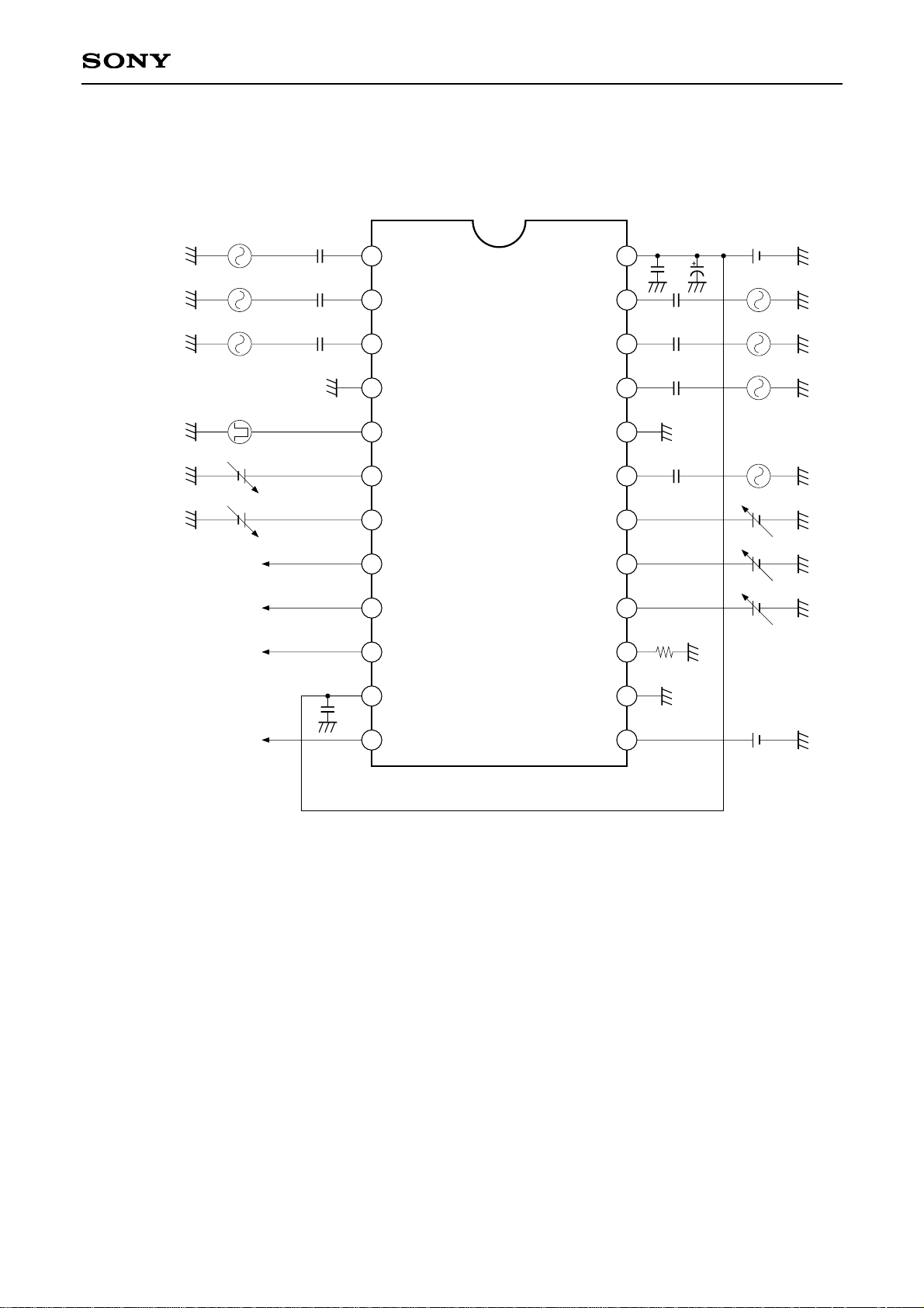
Electrical Characteristics Measurement Circuit
0.1µ
0.01µ 47µ
0.1µ
0.1µ
0.1µ
0/3V
0V to 9V
0V to 9V
10k
0/3V
0.01µ
Y output
R-Y output
B-Y output
Main Y output
0.1µ
0.1µ
0.1µ
0/3V
0/9V
9V
13
14
15
16
17
18
19
20
21
22
23
24
11
12
2
3
4
5
6
7
8
9
10
1
V
CC
Y2 IN
RY2 IN
BY2 IN
GND
TV IN
Y SW
HUE
COLOR
DLY
GND
DLY SW
Y1 IN
RY1 IN
BY1 IN
GND
CLAMP
YUV SW
LEVEL
Y OUT
RY OUT
BY OUT
V
CC
TV OUT
∗
When performing measurements with signals input from Y1 IN, RY1 IN and BY1 IN: YUV
SW = 3V
When performing measurements with signals input from Y2 IN, RY2 IN and BY2 IN: YUV
SW = 0V
Page 8
– 8 –
CXA2039M
Description of Operation
The Y, R-Y and B-Y signals input from Pins 1, 2, 3, 21, 22 and 23 are clamped by the clamp circuit and sent to
the YUV SW circuit. The Y signal input from Pin 19 is clamped by the clamp circuit and then sent to the Y SW
circuit.
The YUV SW circuit receives the switching signal from Pin 6 and selects either the signals from Pins 1, 2 and 3
or from Pins 21, 22 and 23. The R-Y and B-Y signals output from the YUV SW circuit are attenuated and sent
to the delay line and delay switch circuits. The delay time at the delay line circuit can be set as desired in the
range of 500 to 700ns according to the resistance value connected between Pin 15 and GND. After passing
through the delay line circuit, the signals are sent to the delay switch circuit where the Pin 13 control voltage is
received and delay on/off switching is performed. The signals output from the delay switch circuit are input to
the base band hue and color control circuits where the Pins 16 and 17 control voltages are received and hue
and color control is performed. Then, the signals are amplified by the drive circuit and output from Pins 9 and
10. The drive circuit gain can be switched between two values according to the voltage applied to Pin 7. Two
types of Y signals, 0dB and –6dB with respect to the input level, are output from the YUV SW circuit. The 0dB
signal is sent as is to the Y SW circuit, and the –6dB signal is output from Pin 8.
The Y SW circuit receives the switching signal from Pin 18 and selects the Pin 19 signal and either the Pin 1 or
Pin 23 signal selected by YUV SW. Two types of Y signals, an unadjusted signal and a signal attenuated by
–6dB, are output from the Y SW circuit. These signals are sent to the level switch circuit where one of them is
selected according to the voltage applied to Pin 7 and output from Pin 12.
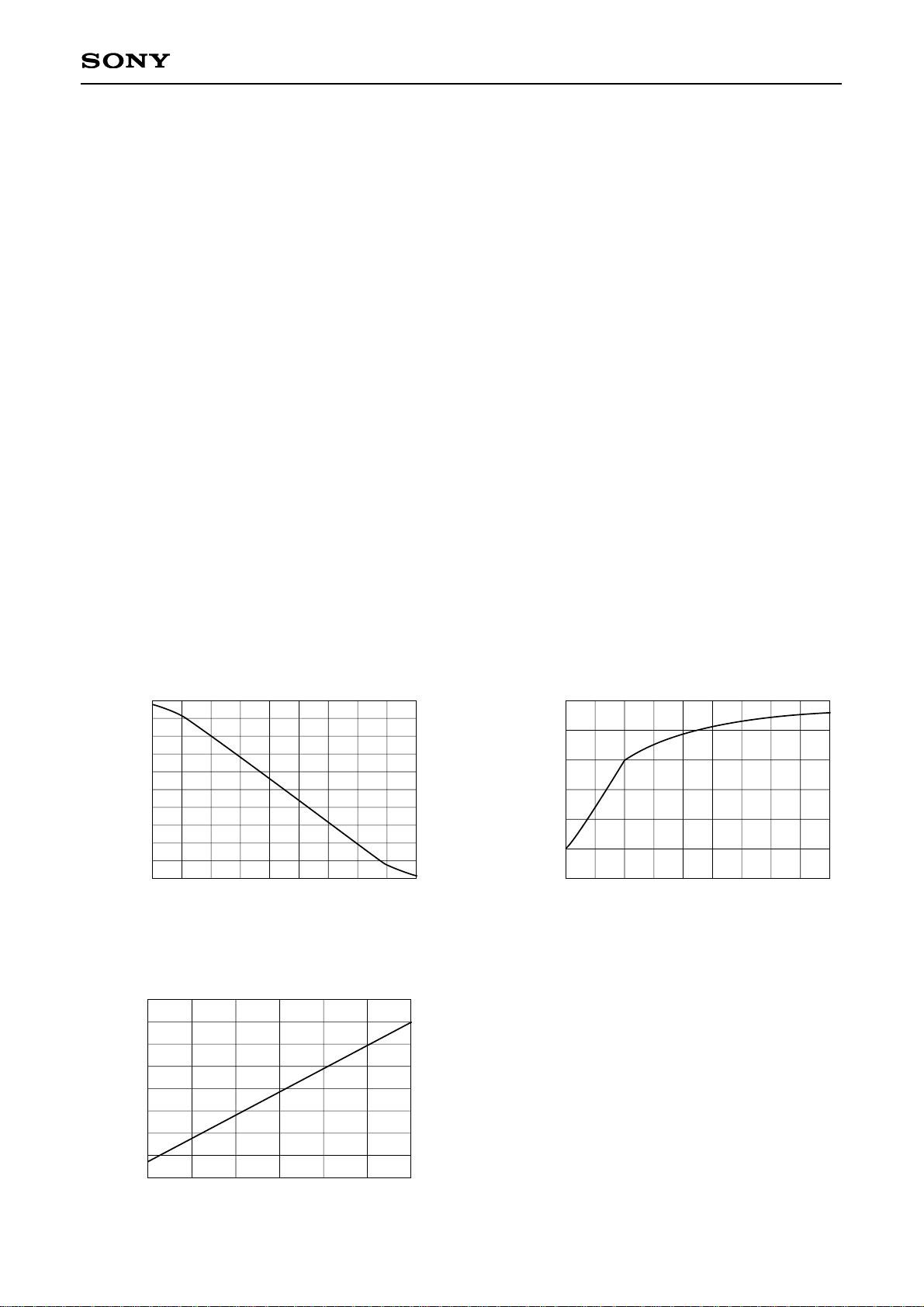
Curve Data
Hue control voltage [V]
0
2684
Hue [deg]
–40
–20
0
20
40
Hue
Color control voltage [V]
02 684
Output gain [dB]
–40
–20
–10
0
10
Color
–50
–30
IREF resistance [kΩ]
68 1210
Delay [ns]
400
500
600
700
I/O delay
7119
450
550
650
750
350
Page 9
– 9 –
CXA2039M
0.1µ
0.01µ 47µ
0.1µ
0.1µ
0.1µ
10k
0.01µ
Y output
R-Y output
B-Y output
Main Y output
0.1µ
0.1µ
0.1µ
13
14
15
16
17
18
19
20
21
22
23
24
11
12
2
3
4
5
6
7
8
9
10
1
V
CC
Y2 IN
RY2 IN
BY2 IN
GND
TV IN
Y SW
HUE
COLOR
DLY
GND
DLY SW
Y1 IN
RY1 IN
BY1 IN
GND
CLAMP
YUV SW
LEVEL
Y OUT
RY OUT
BY OUT
V
CC
TV OUT
B-Y1 input
R-Y1 input
Y1 input
Clamp Pulse input
Y/B-Y/R-Y
switching signal input
Y2 input
R-Y2 input
B-Y2 input
9V
Main Y input
Y switching signal input
(TV IN and Y1 IN/Y2 IN
switching)
Delay = 600ns
Delay increases as
resistance increases
Control DC (0 to 9V)
Delay on/off
signal input
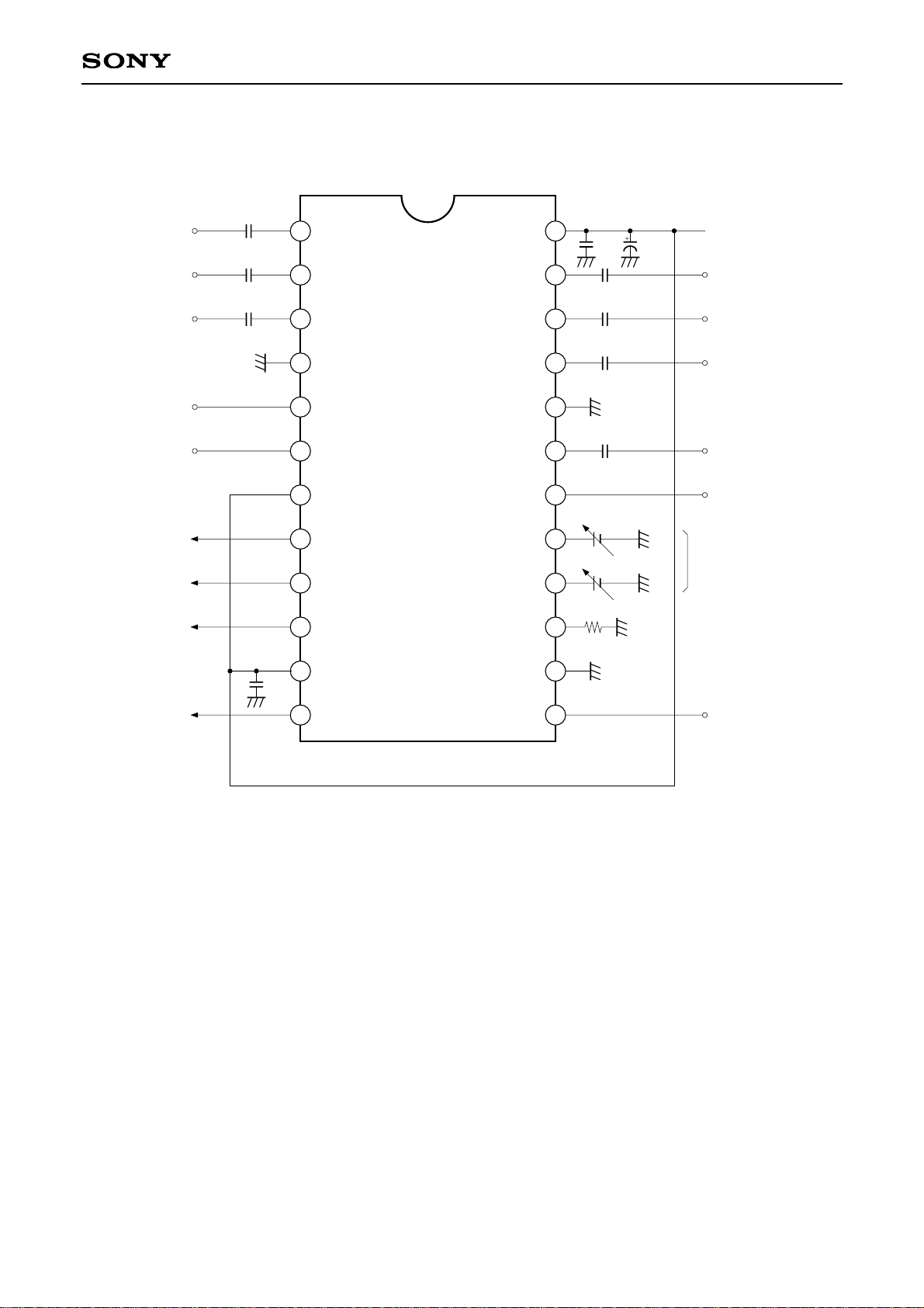
Application Circuit
Pin 7 (Pins 9, 10 and 12 output level switching)
9V = Output High MODE [RYOUT: –2.3dB (Typ.)/BYOUT: –4.7dB (Typ.)]
0V = Output Low MODE [RYOUT: –3.1dB (Typ.)/BYOUT: –5.3dB (Typ.)]
Application circuits shown are typical examples illustrating the operation of the devices. Sony cannot assume responsibility for
any problems arising out of the use of these circuits or for any infringement of third party patent and other right due to same.
Page 10
– 10 –
CXA2039M
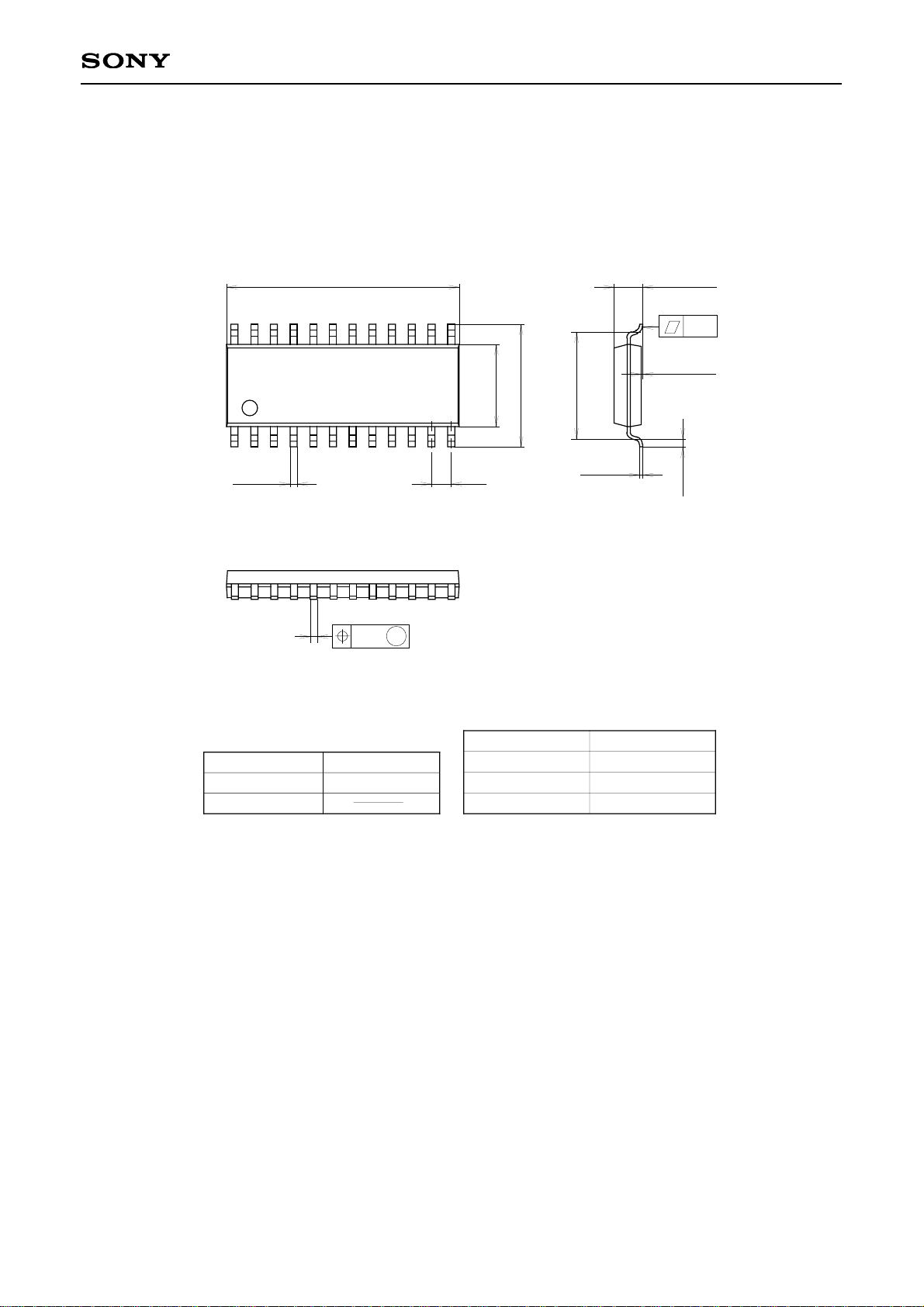
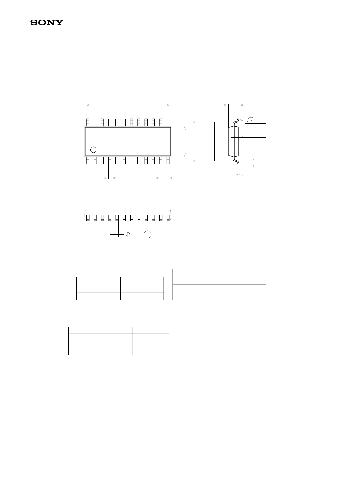
Package Outline Unit: mm
SONY CODE
EIAJ CODE
JEDEC CODE
M
PACKAGE STRUCTURE
MOLDING COMPOUND
LEAD TREATMENT
LEAD MATERIAL
PACKAGE WEIGHT
EPOXY/PHENOL RESIN
SOLDER PLATING
COPPER ALLOY / 42ALLOY
24PIN SOP (PLASTIC)
15.0 – 0.1
+ 0.4
112
1324
1.270.45 ± 0.1
5.3 – 0.1
+ 0.3
7.9 ± 0.4
0.2 – 0.05
+ 0.1
0.5 ± 0.2
0.1 – 0.05
+ 0.2
0.15
1.85 – 0.15
+ 0.4
6.9
± 0.12
SOP-24P-L01
∗SOP024-P-0300-A
0.3g
Page 11
– 11 –
CXA2039M
Sony Corporation
Package Outline Unit: mm
SONY CODE
EIAJ CODE
JEDEC CODE
M
PACKAGE STRUCTURE
MOLDING COMPOUND
LEAD TREATMENT
LEAD MATERIAL
PACKAGE WEIGHT
EPOXY/PHENOL RESIN
SOLDER PLATING
COPPER ALLOY / 42ALLOY
24PIN SOP (PLASTIC)
15.0 – 0.1
+ 0.4
112
1324
1.270.45 ± 0.1
5.3 – 0.1
+ 0.3
7.9 ± 0.4
0.2 – 0.05
+ 0.1
0.5 ± 0.2
0.1 – 0.05
+ 0.2
0.15
1.85 – 0.15
+ 0.4
6.9
± 0.12
SOP-24P-L01
∗SOP024-P-0300-A
0.3g
LEAD PLATING SPECIFICATIONS
ITEM
LEAD MATERIAL COPPER ALLOY
SOLDER COMPOSITION Sn-Bi Bi:1-4wt%
PLA TING THICKNESS 5-18µm
SPEC.
 Loading...