

Page 1
– 1 –
CXA2074Q/S
E96843B86
US Audio Multiplexing Decoder
Description
The CXA2074Q/S is an IC designed as a decoder
for the Zenith TV Multi-channel System and also
corresponds with I2C BUS. Functions include stereo
demodulation, SAP (Separate Audio Program)
demodulation, dbx noise reduction and sound
processor. Various kinds of filters are built in while
adjustment, mode control and sound processor
control are all executed through I2C BUS.
Features
• Audio multiplexing decoder, dbx noise reduction
decoder and sound processor are all included in a
single chip. Almost any sort of signal processing is
possible through this IC.
• All adjustments are possible through I2C BUS to
allow for automatic adjustment.
• Various built-in filter circuits greatly reduce external
parts.
• There are three systems for inputs and two
systems for outputs, and each mode control is
possible.
Standard I/O Level
[( ) is the pin No. for the CXA2074S.]
• Input level
COMPIN (Pin 17) 245mVrms
AUX1-L/R (Pins 36 and 35) 490mVrms
AUX2-L/R (Pins 38 and 37) 490mVrms
• Output level
LPOUT-L/R (Pins 40 and 39) 490mVrms
LSOUT-L/R (Pins 8 and 7) 490mVrms
Absolute Maximum Ratings (Ta = 25°C)
• Supply voltage VCC 11 V
• Operating temperature Topr –20 to +75 °C
• Storage temperature Tstg –65 to +150 °C
• Allowable power dissipation
PD 0.6 (48 pin QFP) W
2.2 (42 pin SDIP) W
Range of Operating Supply Voltage
9 ± 0.5 V
Applications
TV, VCR and other decoding systems for US audio
multiplexing TV broadcasting
Structure
Bipolar silicon monolithic IC
∗ A license of the dbx-TV noise reduction system is
required for the use of this device.
Sony reserves the right to change products and specifications without prior notice. This information does not convey any license by
any implication or otherwise under any patents or other right. Application circuits shown, if any, are typical examples illustrating the
operation of the devices. Sony cannot assume responsibility for any problems arising out of the use of these circuits.
CXA2074Q
48 pin QFP (Plastic)
CXA2074S
42 pin SDIP (Plastic)
Page 2
– 2 –
CXA2074Q/S
AUX1-L
AUX1-R
VCAWGT
VCATC
VCAIN
VEOUT
VEWGT
VE
SAPIN
SAPOUT
STIN
SUBOUT
V
CC
VETC
NOISETC
TRER
TREL
SDA
SCL
DGND
MAININ
MAINOUT
PCINT2
PLINT
COMPIN
VGR
IREF
GND
SAPTC
PCINT1
BASSR1
BASSR2
BASSL1
BASSL2
LSOUT-R
LSOUT-L
LPIN-L
LPIN-R
LPOUT-L
AUX2-L
AUX2-R
LPOUT-R
1
2
3
4
5
6
7
8
9
10
11
12
13
14 15
16
17
18
19
20
21
22
23
24
25
26
27
28
29
30
31
32
33
34
35
36
37
38
39
40
41
42
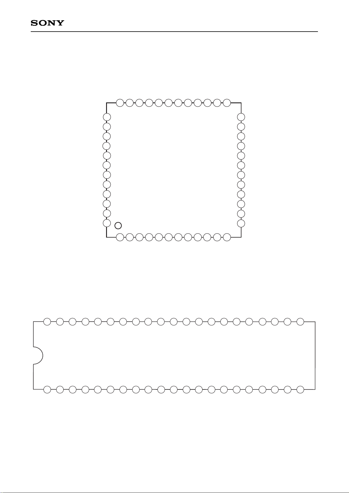
Pin Configuration (Top View)
CXA2074Q
CXA2074S
25
26
27
28
29
30
36
35
34
31
32
33
AUX1-L
AUX1-R
NC
VCAWGT
VCATC
VCAIN
VEOUT
NC
VETC
VEWGT
VE
SAPIN
2
3
4
5
6
7
8
9
10
11
121
TREL
LSOUT-R
LSOUT-L
SCL
DGND
NC
PCINT2
NC
MAINOUT
MAININ
SDA
PCINT1
13
14
15
16
17
18
19
20
21
22
23
24
PLINT
COMPIN
IREF
GND
SAPTC
NC
STIN
NOISETC
VGR
V
CC
SAPOUT
SUBOUT
40
39
38
37
41
42
43
44
45
46
47
48
TRER
BASSL2
BASSL1
BASSR2
LPOUT-L
BASSR1
LPIN-L
LPIN-R
LPOUT-R
AUX2-L
AUX2-R
NC
Page 3
– 3 –
CXA2074Q/S
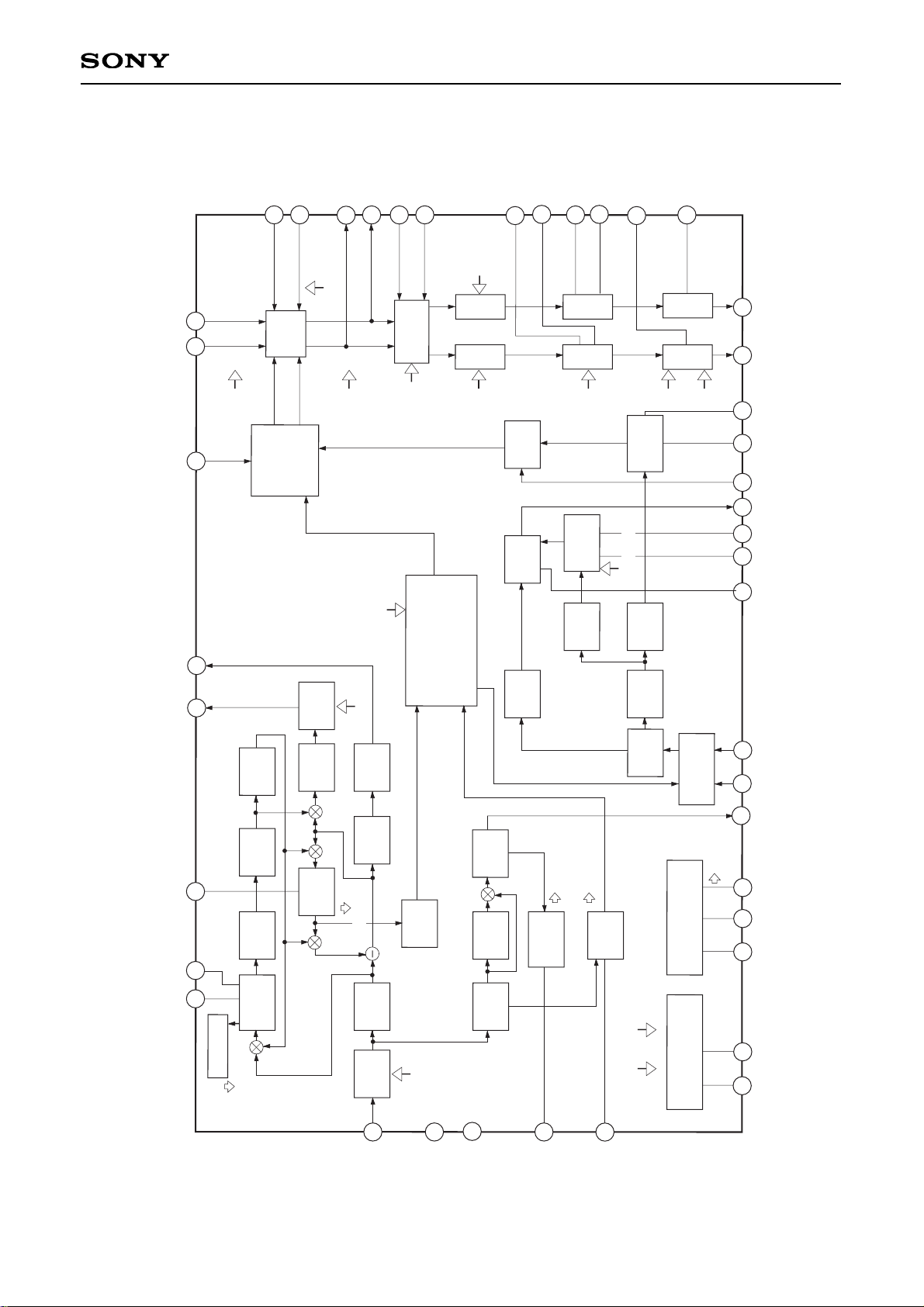
Block Diagram
CXA2074Q
VGR
IREF
DGND
SCL
SDA
SAPOUT
SAPIN
STIN
VE
VEWGT
VETC
VEOUT
VCAIN
VCAWGT
VCATC
MAININ
MAINOUT
SUBOUT
PLINT
PCINT1
COMPIN
V
CC
GND
NOISETC
SAPTC
AUX2-L
IREF
SW
LPF LPF
HPF
RMSDET
RMSDET
VCAVEDeEm
LOGIC
MATRIX
VCA
LPF
LPF
1/21/4VCOLFLT
STLPF
"FILTER"
VCA LPF
BPF
SAPVCO
LPF
NOISE
DET
SAPIND
"PONRES"
STIND
"SAP"
"NOISE"
VCO
NRSW/FOMO/SAPC
WIDEBAND
SPECTRAL
"STEREO"
DeEm
FLT
AMP
(+4dB)
I
2
C BUS I/F
(+6dB)
LSOUT-L
LSOUT-R
M2
TREBLE
TREB
TREB
BASS
PASSSW
BASS
BASS
AUX1-R
AUX1-L
AUX2-R
BASSL1
BASSL2
BASSR1
BASSR2
FILTER
PCINT2
VOL-R
VOL-L
VOL-L
TVSW
LPIN-L
LPIN-R
LPOUT-L
LPOUT-R
FEXT2
FEXT1
TVSW/EXT/M1
TREL
TRER
VOL-R
36
35
38
37
40
39
42
41
ATT
2
3
32
33
31
30
28
2726
48
1
45
44
47
46
8
9
21
13
12
11
14
19
17
23
18
15
16
6
5
4
24
25
22
PSW
Page 4
VGR
IREF
DGND
SCL
SDA
SAPOUT
SAPIN
STIN
VE
VEWGT
VETC
VEOUT
VCAIN
VCAWGT
VCATC
MAININ
MAINOUT
SUBOUT
PLINT
PCINT1
COMPIN
V
CC
GND
NOISETC
SAPTC
AUX2-L
HPF
RMSDET
1/21/4VCOLFLT
"FILTER"
"PONRES"
"SAP"
"NOISE"
NRSW/FOMO/SAPC
WIDEBAND
SPECTRAL
"STEREO"
(+6dB)
LSOUT-L
LSOUT-R
M2
TREBLE
TREB
TREB
BASS
BASS
BASS
AUX1-R
AUX1-L
AUX2-R
BASSL1
BASSL2
BASSR1
BASSR2
PCINT2
VOL-R
VOL-L
VOL-L
IREF
SW
LPF LPF
RMSDET
VCAVEDeEm
LOGIC
MATRIX
VCA
LPF
LPF
STLPF
VCA LPF
BPF
SAPVCO
LPF
NOISE
DET
SAPIND
STIND
VCO
DeEm
FLT
AMP
(+4dB)
I
2
C BUS I/F
PASSSW
FILTER
TVSW
LPIN-L
LPIN-R
LPOUT-L
LPOUT-R
FEXT2
FEXT1
TVSW/EXT/M1
TREL
TRER
VOL-R
3
4
1
2
8
7
ATT
6
5
33
32
34
31
30
29
28
24
27
26
18
19
11
10
9
14
15
16
23
13
12
36
35
17
22
20
25
21
38
37
39
42
41
40
PSW
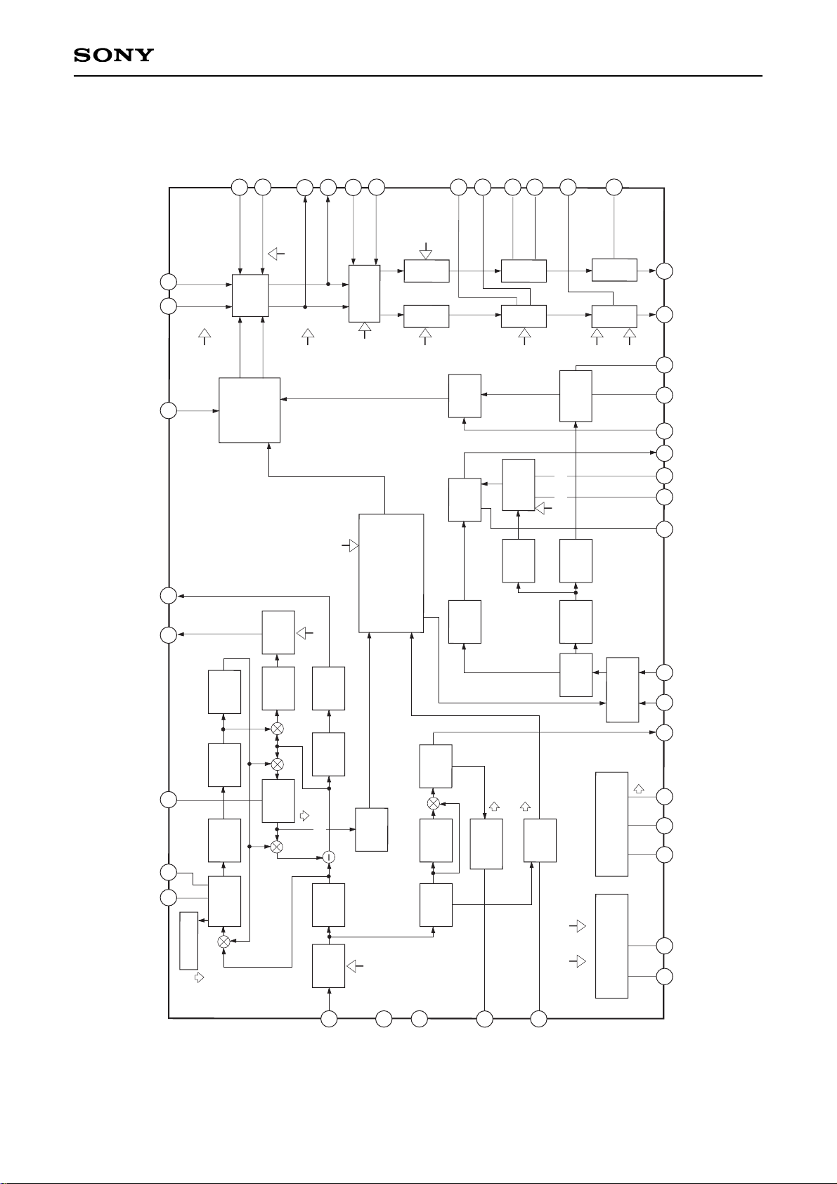
– 4 –
CXA2074Q/S
CXA2074S
Page 5
– 5 –
CXA2074Q/S
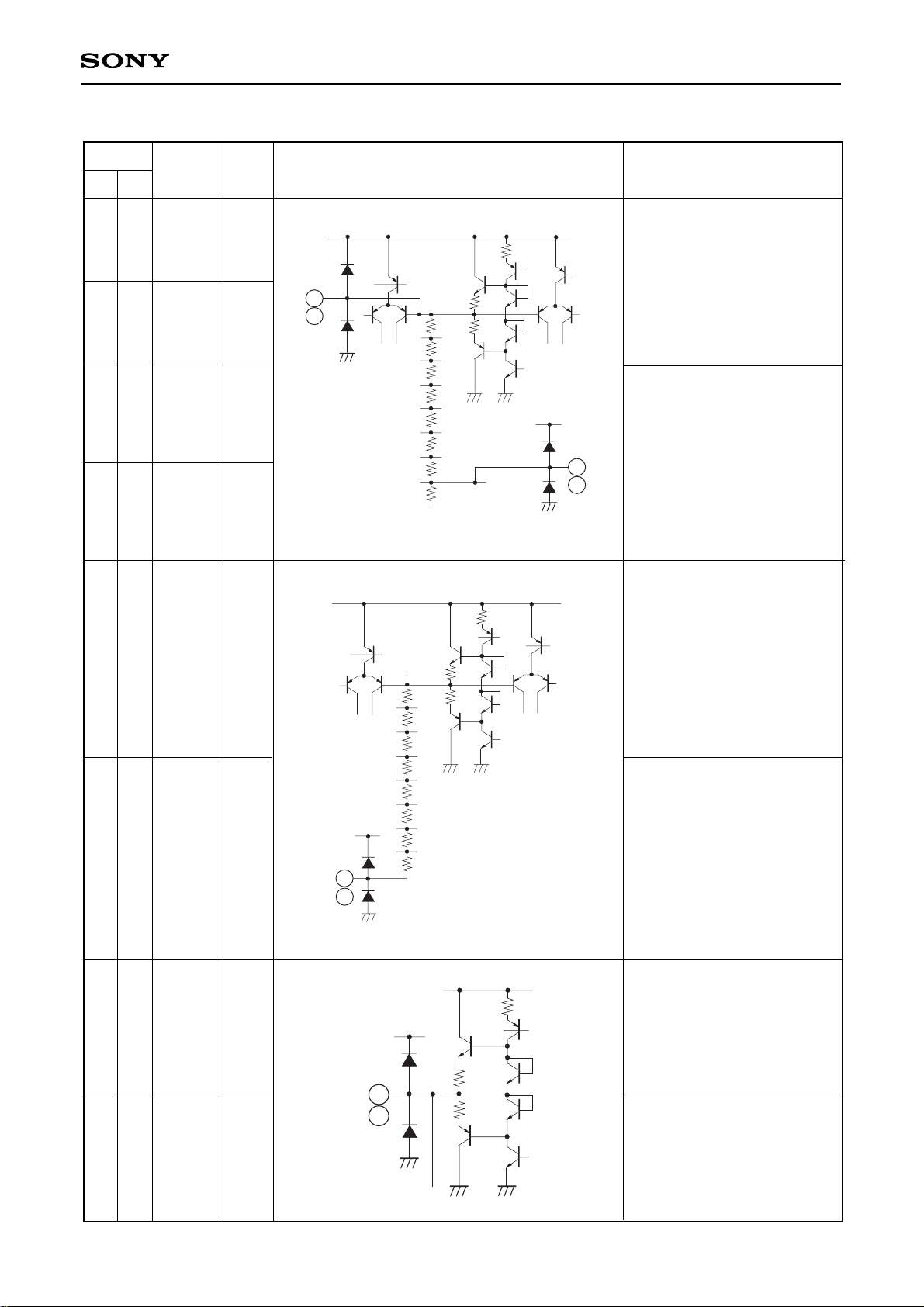
BASSR1
BASSR2
BASSL1
BASSL2
TRER
TREL
LSOUT-R
LSOUT-L
4.0V
4.0V
4.0V
4.0V
4.0V
4.0V
4.0V
4.0V
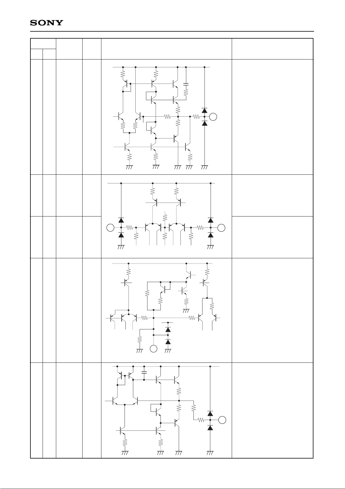
BASS filter pin. (Right channel)
(Connect a 47nF capacitor
between Pins 1 and 2 (44
and 45).)
The cutoff frequency is
determined by the built-in
resistor and the external
capacitance.
BASS filter pin. (Left channel)
(Connect a 47nF capacitor
between Pins 3 and 4 (46
and 47).)
The cutoff frequency is
determined by the built-in
resistor and the external
capacitance.
TREBLE filter pin.
(Right channel)
(Connect a 6.8nF capacitor
between this pin and GND.)
TREBLE filter pin.
(Left channel)
(Connect a 6.8nF capacitor
between this pin and GND.)
LSOUT right channel output
pin.
LSOUT left channel output
pin.
190
190
3k
4V
VCC
4.2k
3.4k
2.7k
2.2k
1.8k
1.4k
1.2k
4.9k
VCC
2
4
1
3
(45)
(47)
(44)
(46)
580
580
3k
VCC
4.2k
3.4k
2.7k
2.2k
1.8k
1.4k
1.2k
4.9k
VCC
5
6
(48)
(1)
580
580
VCC
VCC
3k
7
8
(2)
(3)
44
45
46
47
48
1
2
3
1
2
3
4
5
6
7
8
Pin No.
QFP
SDIP
Symbol
Pin
voltage
Equivalent circuit
Description
Pin Description
Page 6
– 6 –
CXA2074Q/S
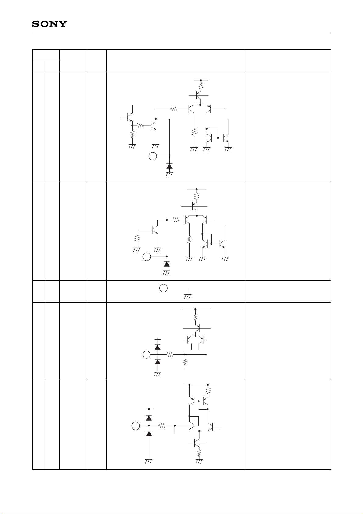
4
5
6
8
9
9
10
11
12
13
SDA
SCL
DGND
MAININ
MAINOUT
—
—
—
4.0V
4.0V
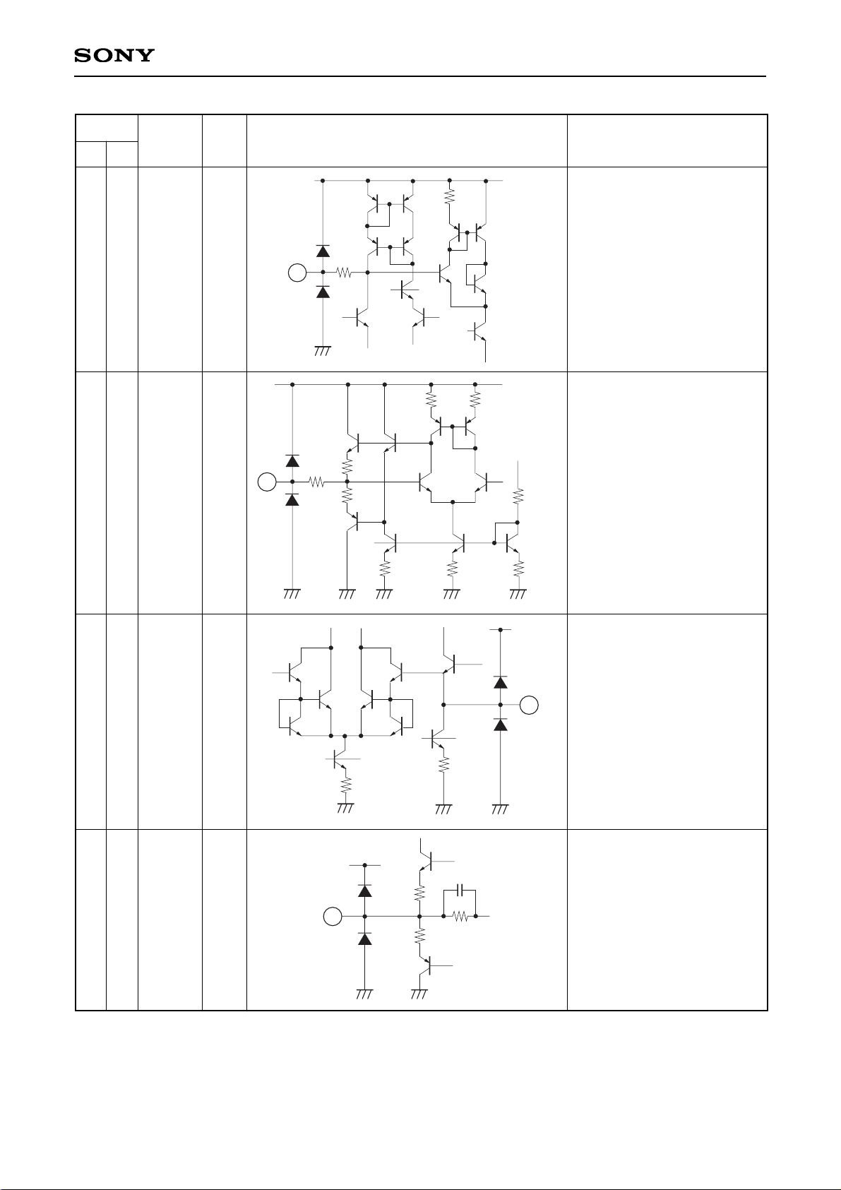
Serial data I/O pin.
VIH >0V
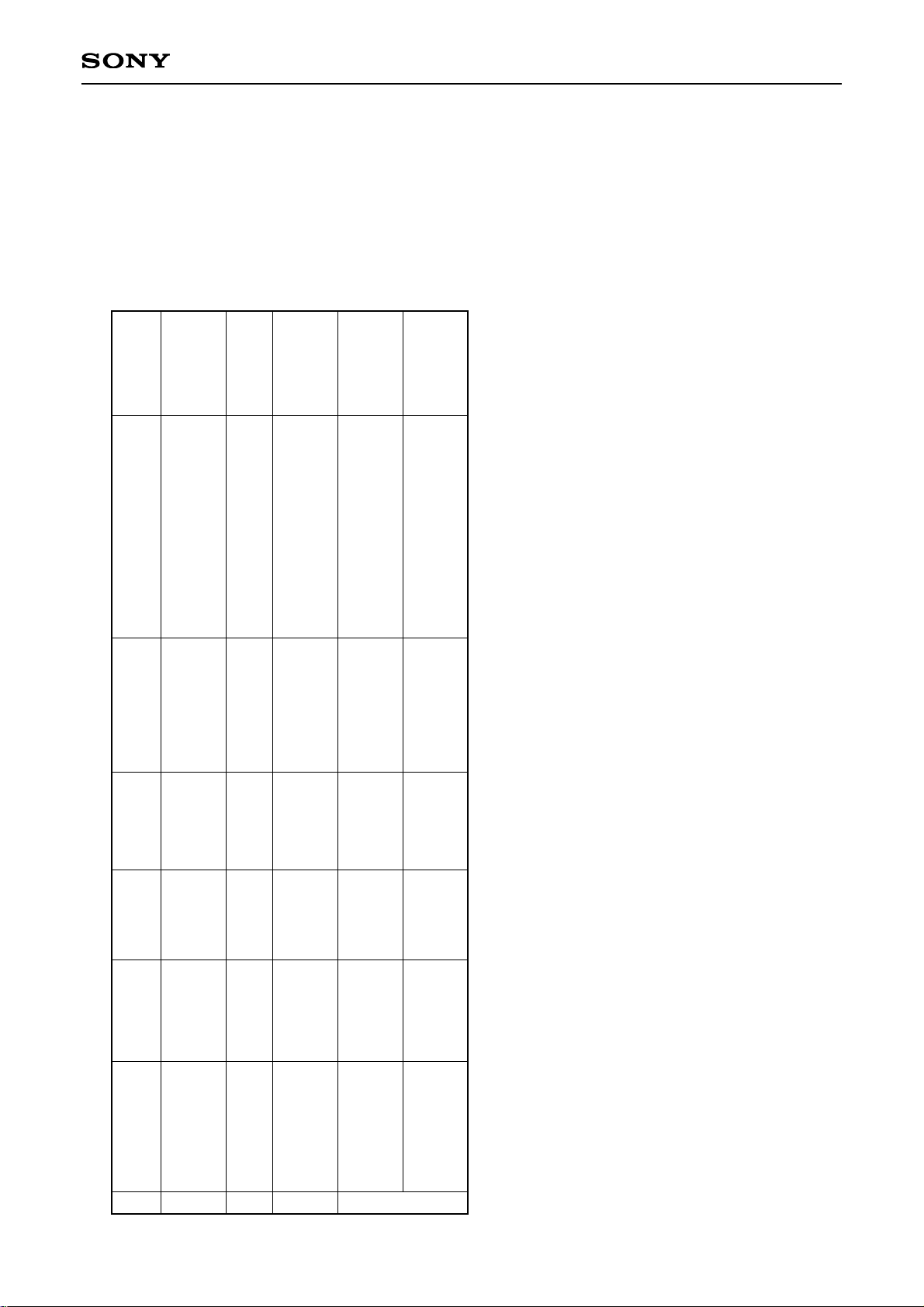
VIL < 1.5V
Serial clock input pin.
VIH >3.0V
VIL < 1.5V
Digital block GND.
Input the (L + R) signal from
MAINOUT (Pin 13 (9)).
(L + R) signal output pin.
7.5k
4.5k
× 5
4k
3k
7.5k
V
CC
↓ 35µ
2.1V
× 2
9
(4)
7.5k
↓ 35µ
2.1V
10.5k
× 4
4k
3k
VCC
10
(5)
11
(6)
VCC
147
10k
53k
4V
VCC
12
(8)
VCC
147
1k
15k
↓
200µ
V
CC
× 4
13
(9)
Pin No.
QFP
SDIP
Symbol
Pin
voltage
Equivalent circuit
Description
Page 7
– 7 –
CXA2074Q/S
11
12
13
14
14
15
16
17
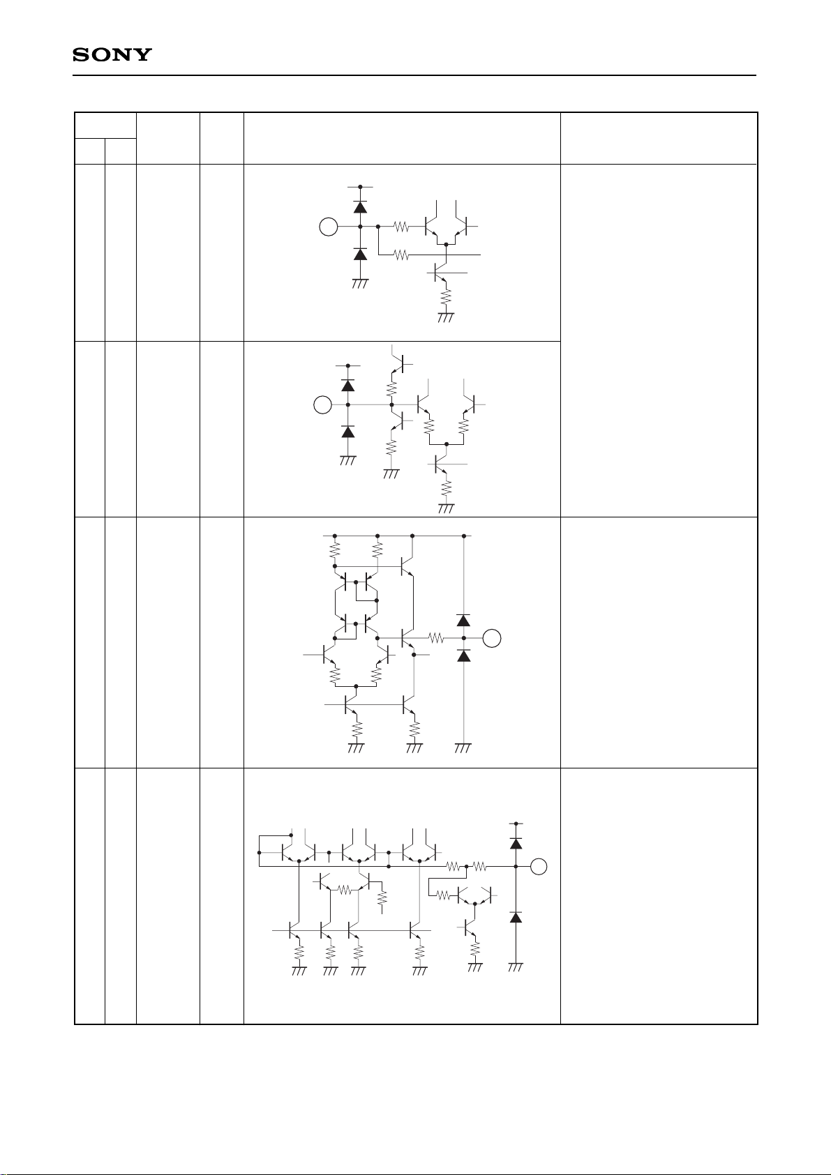
PCINT1
PCINT2
PLINT
COMPIN
4.0V
4.0V
5.1V
4.0V
Stereo block PLL loop filter
integrating pin.
Pilot cancel circuit loop filter
integrating pin.
(Connect a 1µF capacitor
between this pin and GND.)
Audio multiplexing signal
input pin.
VCC
147
20k
↓
26µ
20k
10k
20k
↓
50µ
20k
20k
16
(13)
VCC
22k
3V
20k
4k 4k 4k 16k
24k
50k 147
3k
17
(14)
22k
VCC
30k
147
14
(11)
4k
VCC
× 2
10k
10k
2k
147
15
(12)
Pin No.
QFP
SDIP
Symbol
Pin
voltage
Equivalent circuit
Description
Page 8
– 8 –
CXA2074Q/S
15
16
17
18
19
18
19
20
21
22
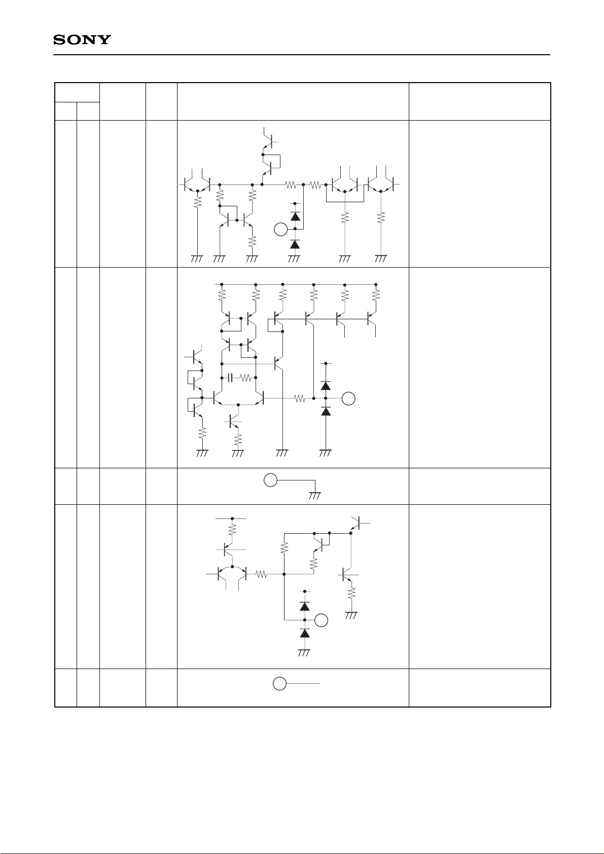
VGR
IREF
GND
SAPTC
VCC
1.3V
1.3V
—
4.5V
—
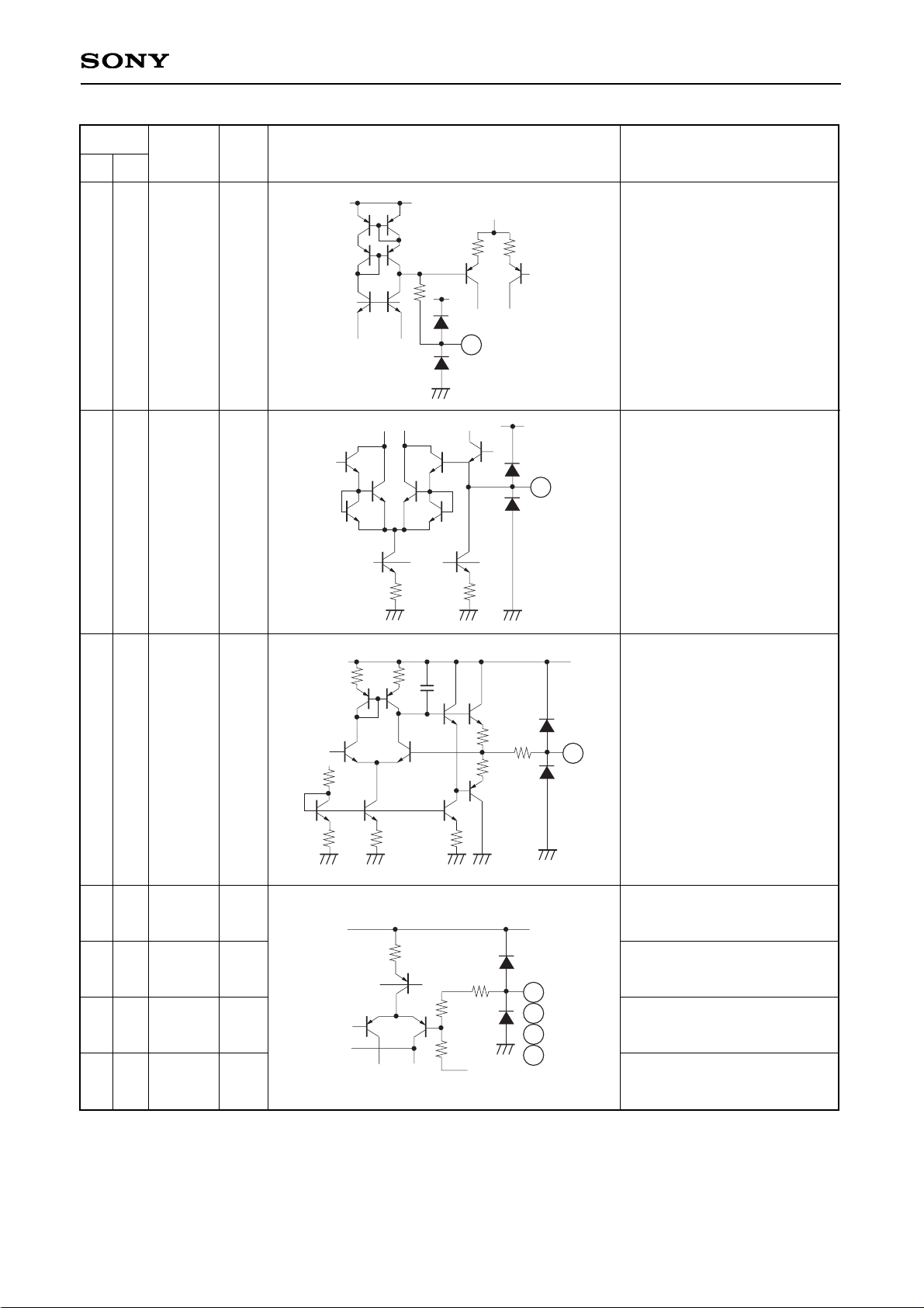
Band gap reference output
pin.
(Connect a 10µF capacitor
between this pin and GND.)
Set the filter and VCO
reference current. The
reference current is adjusted
with the BUS DATA based
on the current which flows to
this pin.
(Connect a 62kΩ (±1%)
resistor between this pin and
GND.)
Analog block GND.
Set the time constant for the
SAP carrier detection circuit.
(Connect a 4.7µF capacitor
between this pin and GND.)
Supply voltage pin.
8k
4k
3k
10k
V
CC
↓ 50µ
1k
VCC
21
(18)
22
(19)
20
(17)
40k 40k 30k
30p 1.8k
16k
6.3k
147
30k 15k 30k
VCC
× 2
V
CC
19
(16)
× 4
11k
9.7k
19.4k
2.06k
3k
147
VCC
11k
11k
18
(15)
Pin No.
QFP
SDIP
Symbol
Pin
voltage
Equivalent circuit
Description
Page 9
– 9 –
CXA2074Q/S
21
22
25
23
24
23
24
27
25
26
SUBOUT
STIN
SAPIN
NOISETC
SAPOUT
4.0V
4.0V
4.0V
3.0V
4.0V
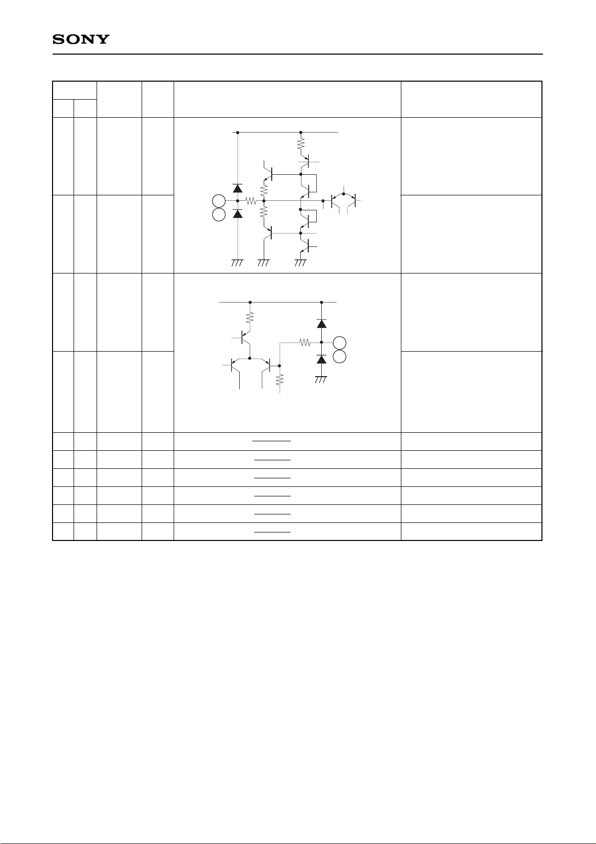
(L – R) signal output pin.
Input the (L – R) signal from
SUBOUT (Pin 23 (21)).
Input the (SAP) signal from
SAPOUT (Pin 26 (24)).
Set the time constant for the
noise detection circuit.
(Connect a 4.7µF capacitor
between this pin and GND.)
SAP FM detector output pin.
23k
147
18k
20k
11.7k
23k
4V
147
18k
4V
VCC
24
27
(22) (25)
3k
3k
3.3k
4k
4V
Vcc
8k
× 2
10k
1k
2k
Vcc
25
200k
(23)
24k
↓ 10µ
580
Vcc
5P
580
4k
↓ 50µ
10k
147
26
(24)
Pin No.
QFP
SDIP
Symbol
Pin
voltage
Equivalent circuit
Description
2k 2k
2k
2k2k
14.4k
4k
580
580
10P
4k
147
1k
Vcc
23
(21)
Page 10
– 10 –
CXA2074Q/S
26
27
28
30
28
29
30
31
VE
VEWGT
VETC
VEOUT
4.0V
4.0V
1.7V
4.0V
Variable de-emphasis
integrating pin.
(Connect a 2700pF capacitor
and a 3.3kΩ resistor in series
between this pin and GND.)
Weight the variable
de-emphasis control
effective value detection
circuit.
(Connect a 0.047µF
capacitor and a 3kΩ resistor
in series between this pin
and GND.)
Determine the restoration
time constant of the variable
de-emphasis control
effective value detection
circuit.
(The specified restoration
time constant can be
obtained by connecting a
3.3µF capacitor between this
pin and GND.)
Variable de-emphasis output
pin.
(Connect a 4.7µF non-polar
capacitor between Pins 31
(30) and 32 (31).)
Vcc
4V
36k
2.9V
580
147
580
8k
30k
↓ 8µ
4k
↓ 50µ
29
(27)
20k
↓ 7.5µ
4k
↓ 50µ
Vcc
× 4
× 4
30
(28)
Vcc
10k
580
580
5P
31
(30)
7.5k
147
VCC
28
(26)
Pin No.
QFP
SDIP
Symbol
Pin
voltage
Equivalent circuit
Description
Page 11
– 11 –
CXA2074Q/S
31
32
33
35
36
37
38
32
33
34
35
36
37
38
VCAIN
VCATC
VCAWGT
AUX1-R
AUX1-L
AUX2-R
AUX2-L
4.0V
1.7V
4.0V
4.0V
4.0V
4.0V
4.0V
VCA input pin.
Input the variable
de-emphasis output signal
from Pin 31 (30) via a
coupling capacitor.
Determine the restoration
time constant of the VCA
control effective value
detection circuit.
(The specified restoration
time constant can be
obtained by connecting a
10µF capacitor between this
pin and GND.)
Weight the VCA control
effective value detection
circuit.
(Connect a 1µF capacitor
and a 3.9kΩ resistor in series
between this pin and GND.)
Right channel external input
1 pin.
Left channel external input
1 pin.
Right channel external input
2 pin.
Left channel external input
2 pin.
4k
VCC
30k 8k
36k
2.9V
3p
580
580
147
40k 40k
↓
50µ
↓
8µ
34
(33)
↓
50µ
VCC
4k
20k
× 4
× 4
↓
7.5µ
33
(32)
VCC
20k
VCC
47k
47k
32
(31)
VCC
4V
27.5k
47k
147
10k
35
36
37
38
Pin No.
QFP
SDIP
Symbol
Pin
voltage
Equivalent circuit
Description
Page 12
– 12 –
CXA2074Q/S
39
40
41
42
7
10
20
29
34
43
39
40
41
42
—
—
—
—
—
—
LPOUT-R
LPOUT-L
LPIN-R
LPIN-L
NC
NC
NC
NC
NC
NC
4.0V
4.0V
4.0V
4.0V
—
—
—
—
—
—
LPOUT right channel output
pin.
LPOUT left channel output
pin.
Right channel loop input pin.
Left channel loop input pin.
VCC
4V
47k
147
10k
41
42
3k
580
580
VCC
39
40
147
Pin No.
QFP
SDIP
Symbol
Pin
voltage
Equivalent circuit
Description
(7)
(10)
(20)
(29)
(34)
(43)
Page 13
– 13 –
CXA2074Q/S
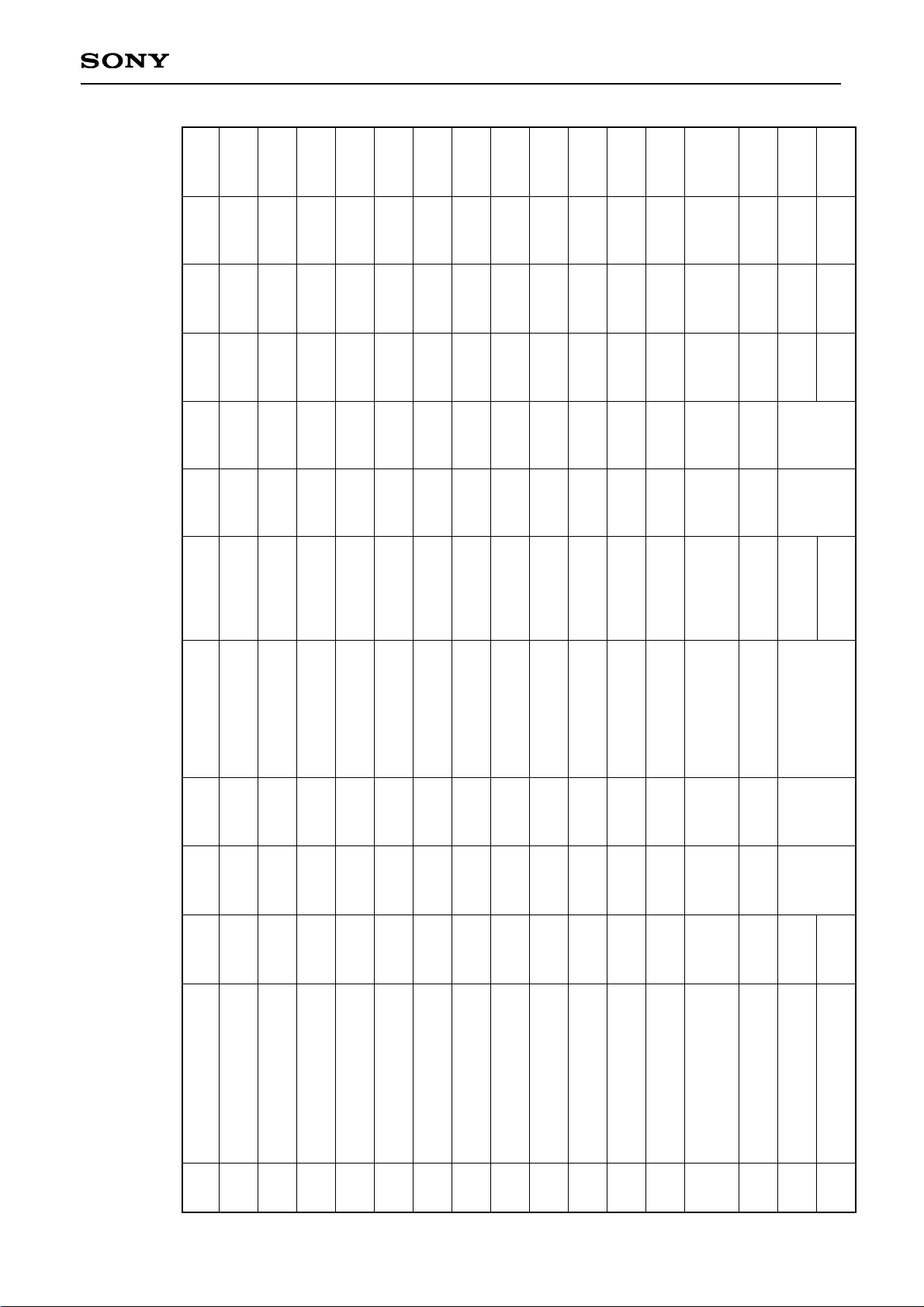
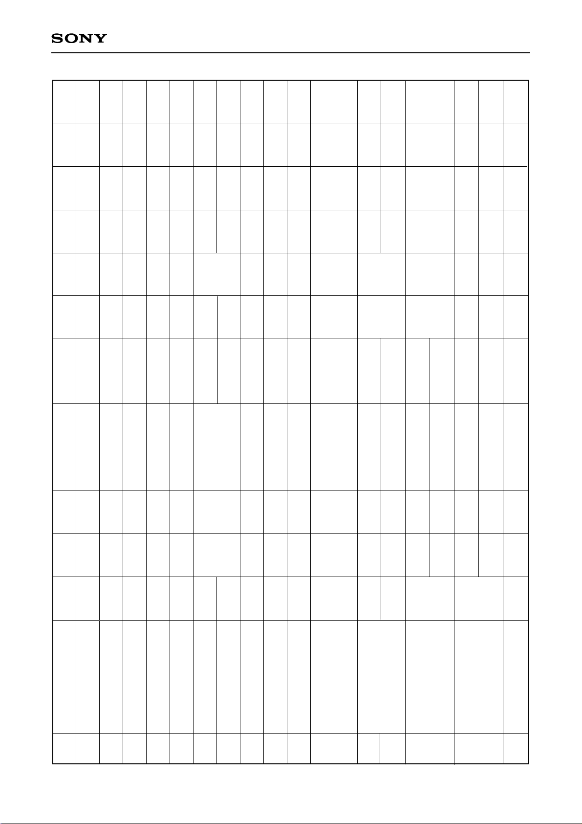
Electrical Characteristics
COMPIN input level
(100% modulation level)
The pin numbers in parenthesis are for the CXA2074Q.
(Ta = 25°C, V
CC = 9V)
Main (L + R) (Pre-Emphasis: OFF) = 245mVrms
SUB (L – R) (dbx-TV: OFF) = 490mVrms
Pilot = 49mVrms
SAP Carrier = 147mVrms
fH = 15.734kHz
Item
Current consumption
Main output level
Main de-emphasis
frequency characteristic
Main LPF frequency
characteristic
Main distortion
Main overload distortion
Main S/N
Sub output level
Sub LPF frequency
characteristic
Sub distortion
Sub overload distortion
Sub S/N
ST → SAP
Crosstalk
Sub pilot leak
Stereo ON level
Stereo ON/OFF
hysteresis
No.
1
2
3
4
5
6
7
8
9
10
11
12
13
14
15
16
Signal
Icc
Vmain
FCdeem
FCmain
THDm
THDmmax
SNmain
Vsub
FCsub
THDsub
THDsmax
SNsub
CTst
PCsub
THst
HYst
Mode
MONO
MONO
MONO
MONO
MONO
MONO
ST
ST
ST
ST
ST
SAP
ST
ST
Input pin
17
(14)17(14)17(14)17(14)17(14)17(14)17(14)17(14)17(14)17(14)17(14)17(14)17(14)17(14)
17
(14)
Min.
30
440
–1.2
–3.0
–
–
61
150
–3.0
–
–
56
60
–
–9.0
3.5
Typ.
40
490
0
–1.0
0.1
0.15
69
190
–0.5
0.1
0.2
64
70
–35
–6.0
6.0
Max.
50
540
1.0
1.0
0.5
0.5
–
230
1.0
1.0
2.0
–
–
–27
–3.0
8.5
Unit
mA
mVrms
dB
dB
%
%
dB
mVrms
dB
%
%
dB
dB
dB
dB
dB
Input signal
No signal
Mono 1kHz 100% mod.
Pre-em. ON
Mono 5kHz 30% mod.
Pre-em. ON
Mono 12kHz 30% mod.
Pre-em. ON
Mono 1kHz 100% mod.
Pre-em. ON
Mono 1kHz 200% mod.
Pre-em. OFF
Mono 1kHz,
Pre-em. ON
SUB (L-R), 1kHz,
100% mod., NR OFF
SUB (L-R) 12kHz,
30% mod., NR OFF
SUB (L-R) 1kHz,
100% mod., NR OFF
SUB (L-R), 1kHz,
200% mod., NR OFF
SUB (L-R) 1kHz,
NR OFF
SUB (L-R), 1kHz,
100% mod., NR ON,
SAP Carrier (5fH)
PILOT (fH) 0dB
Change
PILOT (fH) Level
Measurement
conditions
20 log
('5k'/'1k')
20 log
('12k'/'1k')
20 log
('100%'/'0%')
20 log
('12k'/'1k')
20 log
('100%'/'0%')
20 log
('NRSW = 0'/
'NRSW = 1')
0dB = 49mVrms
0dB = 49mVrms
20 log (‘on
level'/'off level')
Filter
15kLPF
15kLPF
15kLPF
15kLPF
15kLPF
15kLPF
1kBPF
f
H BPF
Output
pin
39/40
39/40
39/40
39/40
39/40
39/40
23
(21)23(21)23(21)23(21)23(21)
40
23
(21)
BUS
RETURN
Page 14
– 14 –
CXA2074Q/S
No.
17
18
19
20
21
22
23
24
25
26
27
28
29
30
31
32
33
Item
SAP output level
SAP LPF frequency
characteristic
SAP distortion
SAP S/N
SAP → ST
Cross talk
SAP ON level
SAP ON/OFF hysteresis
ST separation 1 L → R
ST separation 1 R → L
ST separation 2 L → R
ST separation 2 R → L
LPOUT output level
LPOUT
muted amount
LSOUT output level
LSOUT cross talk
LSOUT muted amount
Symbol
Vsap
FCsap
THDsap
SNsap
CTsap
THsap
HYsap
STLsep1
STRsep1
STLsep2
STRsep2
Vtp
MUlp1
MUlp2
Vls
CTls
MUls
Mode
SAP
SAP
SAP
SAP
ST
SAP
ST
ST
ST
ST
EXT
INT
EXT
INT
EXT
INT
EXT
EXT
Input pin
17
(14)17(14)17(14)17(14)17(14)17(14)
17
(14)17(14)17(14)17(14)
35/36
37/38
17
(14)
35/36
37/38
17
(14)
35/36
37/38
35/36
37/38
17
(14)
35/36
37/38
Min.
150
–3.0
–
46
60
–12.0
2.0
23
23
23
23
–0.5
–
–
–0.9
–
–
–
Typ.
190
0
2.5
55
70
–9.0
4.0
35
35
35
35
0
–85
–90
0
–75
–90
–90
Max.
230
2.5
6.0
–
–
–6.5
6.0
–
–
–
–
0.5
–70
–75
0.9
–60
–80
–75
Unit
mVrms
dB
%
dB
dB
dB
dB
dB
dB
dB
dB
dB
dB
dB
dB
dB
dB
dB
Input signal
SAP 1kHz 100% mod.
NR OFF
SAP 10kHz, 30% mod
.
NR OFF
SAP 1kHz 100% mod
.
NR OFF
SAP 1kHz, NR OFF
SAP 1kHz 100% mod.
NR ON, Pilot (fH)
Change
SAP Carrier (5f
H)
Level
ST-L 300Hz 30% mod
.
NR ON
ST-R 300Hz 30% mod
.
NR ON
ST-L 3kHz 30% mod
.
NR ON
ST-R 3kHz 30% mod
.
NR ON
Sine wave 1kHz,
490mVrms
MONO 1kHz, 100%,
Pre-em. on
Sine wave 1kHz,
490mVrms
MONO 1kHz
100%, Pre-em. on
Sine wave 1kHz,
490mVrms
Sine wave 1kHz,
490mVrms
MONO 1kHz
100%, Pre-em. on
Sine wave 1kHz,
490mVrms
Measurement
conditions
20 log
('10k'/'1k')
20 log
('100%'/'0%')
20 log ('NRSW
= 1'/'NRSW = 0')
0dB = 147mVrms
20 log (‘on
level’/’off level’)
0dB = 490mVrms
20 log
(M1 =
"0"/M1 = "1")
20 log
(M1 =
"0"/M1 = "1")
0dB = 490mVrms
0dB = 490mVrms
0dB = 490mVrms
EXT → INT
0dB=490mVrms
INT → EXT
20 log (M2 =
"0"/M2 = "1")
Filter
15kLPF
15kLPF
1kBPF
15kLPF
15kLPF
15kLPF
15kLPF
1kBPF
1kBPF
1kBPF
1kBPF
Output
pin
26
(24)26(24)26(24)26(24)
40
BUS
RETURN
39/40
39/40
39/40
39/40
39/40
39/40
7/8
(2/3)
7/8
(2/3)
7/8
(2/3)
7/8
(2/3)
Page 15

– 15 –
CXA2074Q/S
No.
34
35
36
37
38
39
40
41
42
Item
LSOUT DC offset
LSOUT distortion
LSOUT S/N
LSOUT overload distortion
BASS maximum value
BASS minimum value
TREBLE maximum value
TREBLE minimum value
Volume minimum value
Symbol
OSls
THDls
SNls
THDlsmax
TBmax
TBmin
TTmax
TTmin
VOLmin
Mode
INT
EXT
EXT
EXT
EXT
EXT
EXT
EXT
EXT
EXT
Input pin
—
35/36
37/38
35/36
37/38
35/36
37/38
35/36
37/38
35/36
37/38
35/36
37/38
35/36
37/38
35/36
37/38
Min.
–25
–
75
–
11
–13
11
–13
–
Typ.
0
0.01
88
0.1
12
–12
12
–12
–90
Max.
25
0.5
–
1.0
13
–11
13
–11
–75
Unit
mV
%
dB
%
dB
dB
dB
dB
dB
Input signal
No signal
Sine wave 1kHz,
490mVrms
Sine wave 1kHz,
490mVrms
Sine wave 1kHz,
2Vrms
Sine wave 100Hz,
245mVrms
Sine wave 100Hz,
245mVrms
Sine wave 10kHz,
245mVrms
Sine wave 10kHz,
245mVrms
Sine wave 1kHz,
490mVrms
Measurement
conditions
Mute (M2 = 0)/
DC difference
when there is
no signal
20 log
('490mVrms'/
'No signal')
BASS = "F"
0dB = 245mVrms
BASS = "0"
0dB = 245mVrms
TREBLE = "F"
0dB = 245mVrms
TREBLE = "0"
0dB = 245mVrms
VOL-L = "0",
VOL-R = "0"
0dB = 490mVrms
Filter
15kLPF
15kLPF
15kLPF
1kBPF
Output
pin
7/8
(2/3)
7/8
(2/3)
7/8
(2/3)
7/8
(2/3)
7/8
(2/3)
7/8
(2/3)
7/8
(2/3)
7/8
(2/3)
7/8
(2/3)
Page 16

– 16 –
CXA2074Q/S
I2C BUS block items (SDA, SCL)
I2C BUS load conditions: Pull-up resistor 4kΩ (Connect to +5V)
Load capacity 200pF (Connect to GND)
I2C BUS Control Signal
1
2
3
4
5
6
7
8
9
10
11
12
13
14
15
16
17
18
High level input voltage
Low level input voltage
High level input current
Low level input current
Low level output voltage SDA (Pin 9) during 3mA inflow
Maximum inflow current
Input capacitance
Maximum clock frequency
Minimum waiting time for data change
Minimum waiting time for start of data transfer
Low level clock pulse width
High level clock pulse width
Minimum waiting time for start preparation
Minimum data hold time
Minimum data preparation time
Rise time
Fall time
Minimum waiting time for stop preparation
VIH
VIL
IIH
IIL
VOL
IOL
CI
fSCL
tBUF
tHD: STA
tLOW
tHIGH
tSU: STA
tHD: DAT
tSU: DAT
tR
tF
tSU: STO
3.0
0
—
—
0
3
—
0
4.7
4.0
4.7
4.0
4.7
0
250
—
—
4.7
—
—
—
—
—
—
—
—
—
—
—
—
—
—
—
—
—
—
5.0
1.5
10
10
0.4
—
10
100
—
—
—
—
—
—
—
1
300
—
V
µA
V
mA
pF
kHz
µs
ns
µs
ns
µs
SDA
SCL
tBUF
P
S
t
HD: STA
t
LOW
tHD: DAT
t
HIGH
tR
tF
tHD: STA
t
SU: STA
Sr
t
SU: STO
P
t
SU: DAT
No. Item Symbol Min. Typ. Max. Unit
Page 17

– 17 –
CXA2074Q/S
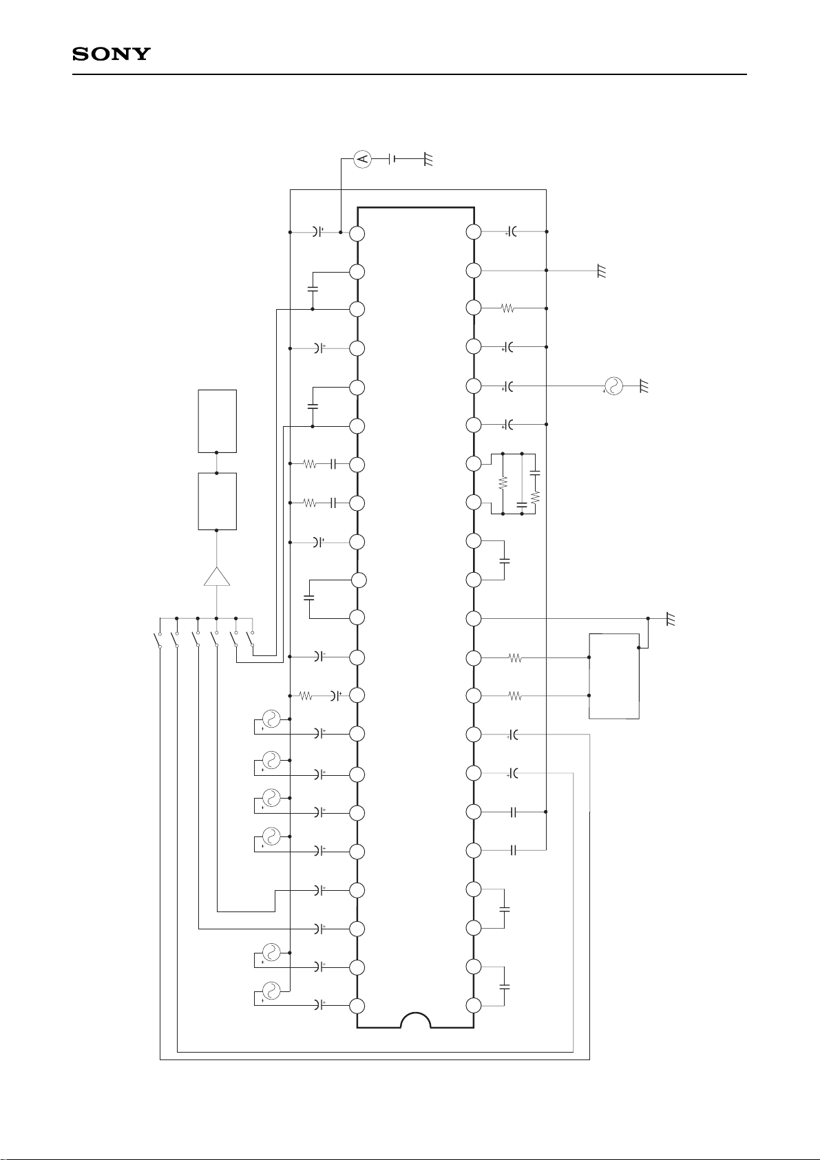
Electrical Characteristics Measurement Circuit
CXA2074Q
MEASURESFILTERS
15kHz LPF
f
H BPF
1kHz BPF
I
2
C BUS DATA
S6
S5
S4
S3
S2
S1
BUFF
R6
3.3k
R4
3k
C19
2700p
C18
0.047µ
25
2627
28
29
30
36
35
34
31
32
33
AUX1-L
AUX1-R
NC
VCAWGT
VCATC
VCAIN
VEOUT
NC
VETC
VEWGT
VE
SAPIN
2
3
4
5
6
7
8
9
10
11
12
1
TREL
LSOUT-R
LSOUT-L
SCL
DGND
NC
PCINT2
NC
MAINOUT
MAININ
SDA
PCINT1
13
14
15
16
17
18
19
20
21
22
23
24
PLINT
COMPIN
IREF
GND
SAPTC
NC
STIN
NOISETC
VGR
V
CC
SAPOUT
SUBOUT
40
39
38
37
41
42
43
44
45
46
47
48
TRER
BASSL2
BASSL1
BASSR2
LPOUT-L
BASSR1
LPIN-L
LPIN-R
LPOUT-R
AUX2-L
AUX2-R
NC
C17
3.3µ
TANTALUM
C15
4.7µ
C14
10µ
TANTALUM
R1
3.9k
C13
1µ
C12
4.7µ
C10
4.7µ
SIGNAL
GENERATOR
V6
AC
V5
AC
V4
AC
V2
AC
SIGNAL
GENERATOR
SIGNAL
GENERATOR
SIGNAL
GENERATOR
C8
47n
V3
AC
SIGNAL
GENERATOR
C1
6.8n
C2
4.7µ
C3
4.7µ
C4
4.7µ
C5
4.7µ
C6
4.7µ
C7
4.7µ
V1
AC
SIGNAL
GENERATOR
C9
47n
C11
6.8n
C16
4.7µ
R2
220R3220
R7
1MEG
C20
5600P
R5
100k
C21
0.012µ
DGND
C29
4.7µ
C26
4.7µ
GND
V7
AC
SIGNAL
GENERATOR
GND
GND
C27
1µ
C25
10µ
R8
62k METAL ± 1%
C24
4.7µ
C23
100µ
V8
9V
V
CC
C22
4.7µ
C28
4.7µ
Page 18
– 18 –
CXA2074Q/S
CXA2074S
I
2
C BUS DATA
DGND
SIGNAL
GENERATO
R
GND
V7
AC
R2
3.9k
C16 10µ
TANTALUM
R5
3k
S1S2S3S
4
BUFF
FILTER
S
MEASURE
S
15kHz LPF
f
H BPF
1kHz BPF
S5S
6
V1
AC
SIGNAL
GENERATOR
SIGNAL
GENERATOR
5
6
7
8
9
10
12
13
15
16
17
18
21
22
25
27
28
29
40
39
34
31
32
33
42
C1
4.7µ
C21
0.047µ
C17
4.7µ
C31
100µ
C30
4.7µ
C27
10µ
C26
4.7µ
C24
1µ
R3
220
R1
220
C13
4.7µ
C11
4.7µ
C9
6.8n
C7
6.8n
20
R8 62k
METAL ± 1%
14
R6
1MEG
C20 5600p
R4
100k
C22
0.012µ
BASSR1
BASSR2
BASSL1
BASSL2
LSOUT-R
LSOUT-L
TRER
TREL
SDA
SCL
DGND
MAININ
MAINOUT
PCINT1
PCINT2
PLINT
COMPIN
VGR
IREF
GND
SAPTC
LPIN-L
LPIN-R
LPOUT-L
LPOUT-R
AUX2-L
AUX2-R
AUX1-L
AUX1-R
VCAWGT
VCATC
VCAIN
VEOUT
VETC
VEWGT
VE
SAPIN
SAPOUT
NOISETC
STIN
SUBOUT
V
CC
C18
4.7µ
11
C5
47n
C2
47n
2
3
4
1
V2
AC
C3
4.7µ
41
SIGNAL
GENERATOR
SIGNAL
GENERATOR
V3
AC
C8
4.7µ
V4
AC
C10
4.7µ
SIGNAL
GENERATOR
V5
AC
C12
4.7µ
V6
AC
C14
4.7µ
SIGNAL
GENERATOR
38
37
36
35
C6
4.7µ
C4
4.7µ
C15
1µ
30
C19 3.3µ
TANTALUM
R7
3.3k
C23
2700p
26
C25
4.7µ
C28
4.7µ
24
C29
4.7µ
GND
GND
V8
9V
V
CC
23
19
Page 19
– 19 –
CXA2074Q/S
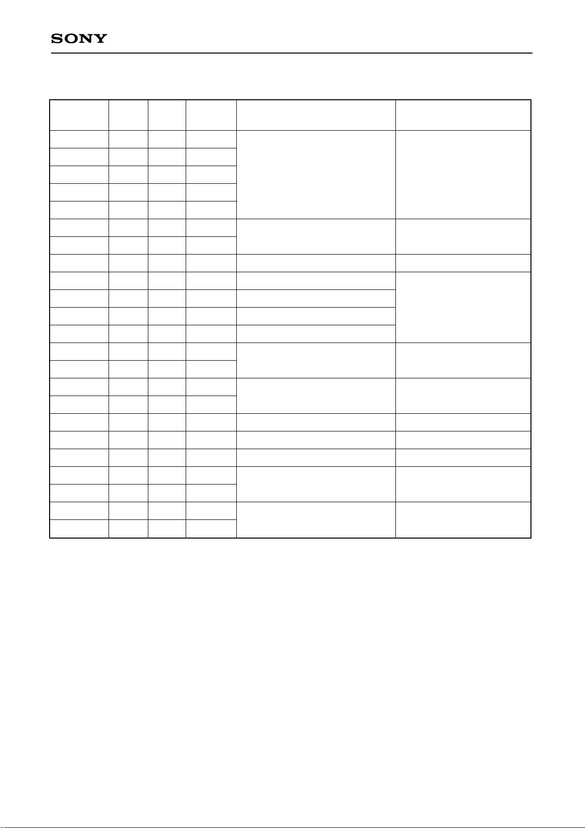
I2C BUS Register Data Standard Setting Values
ATT
VCO
FILTER
SPECTRAL
WIDEBAND
TEST-DA
TEST1
FST
VOL-L
VOL-R
BASS
TREBLE
NRSW
FOMO
TVSW
EXT
FEXT1
FEXT2
PSW
M1
M2
ATTSW
SAPC
4
6
6
6
6
1
1
1
6
6
4
4
1
1
1
1
1
1
1
1
1
1
1
A
A
A
A
A
T
T
T
U
U
U
U
U
U
U
U
U
U
U
U
U
S
S
9
1F
1F
1F
1F
0
0
0
3F
3F
8
8
—
—
0
0
0
0
0
1
1
—
—
Center point
Normal mode
Normal mode
3F = 0dB
3F = 0dB
7 or 8 = 0dB
7 or 8 = 0dB
According to the mode control table
TV decoder output selection
External input 1 forced MONO
External input 2 forced MONO
TVSW output selection
Mute OFF
Fixed by the set specifications
Adjustment point
Standard setting value
FST = 0
Standard setting value
Standard setting value
Standard setting value
Standard setting value
Register
Number
of bits
Classification
Standard
setting
Contents
Setting value when electrical
characteristics are measured
ClassificationA: Adjustment
U: User control
S: Proper to set
T: Test
Page 20
– 20 –
CXA2074Q/S
List of Adjustment Contents The pin numbers in parenthesis are for the CXA2074Q.
1
2
3
4
MAIN VCA
ST & SAP
VCO
ST & SAP
& dbx FILTER
Low frequency
ST separation
High frequency
ST separation
ATT
VCO
FILTER
WIDEBAND
SPECTRAL
COMPIN
Pin 17
(Pin 14)
None
COMPIN
Pin 17
(Pin 14)
COMPIN
Pin 17
(Pin 14)
COMPIN
Pin 17
(Pin 14)
100Hz
245mVrms
None
9.4kHz
600mVrms
ST-L 30%
300Hz
ST-L 30%
3kHz
LPOUT-L output
level
LPOUT-R output
frequency
STA5
(FILADJ)
LPOUT-R output
level
LPOUT-R output
level
Adjust as close to 490mVrms
as possible
Adjust as close to 62.936kHz
as possible
Adjust to the center of the
FILADJ = 1 condition
Minimize the output level
Minimize the output level
TEST-DA = 1
TEST1 = 1
Adjustment item
Adjustment
data
Input pin
Input signal
data
Measurement Adjustment contents
Test mode
setting
Page 21
– 21 –
CXA2074Q/S
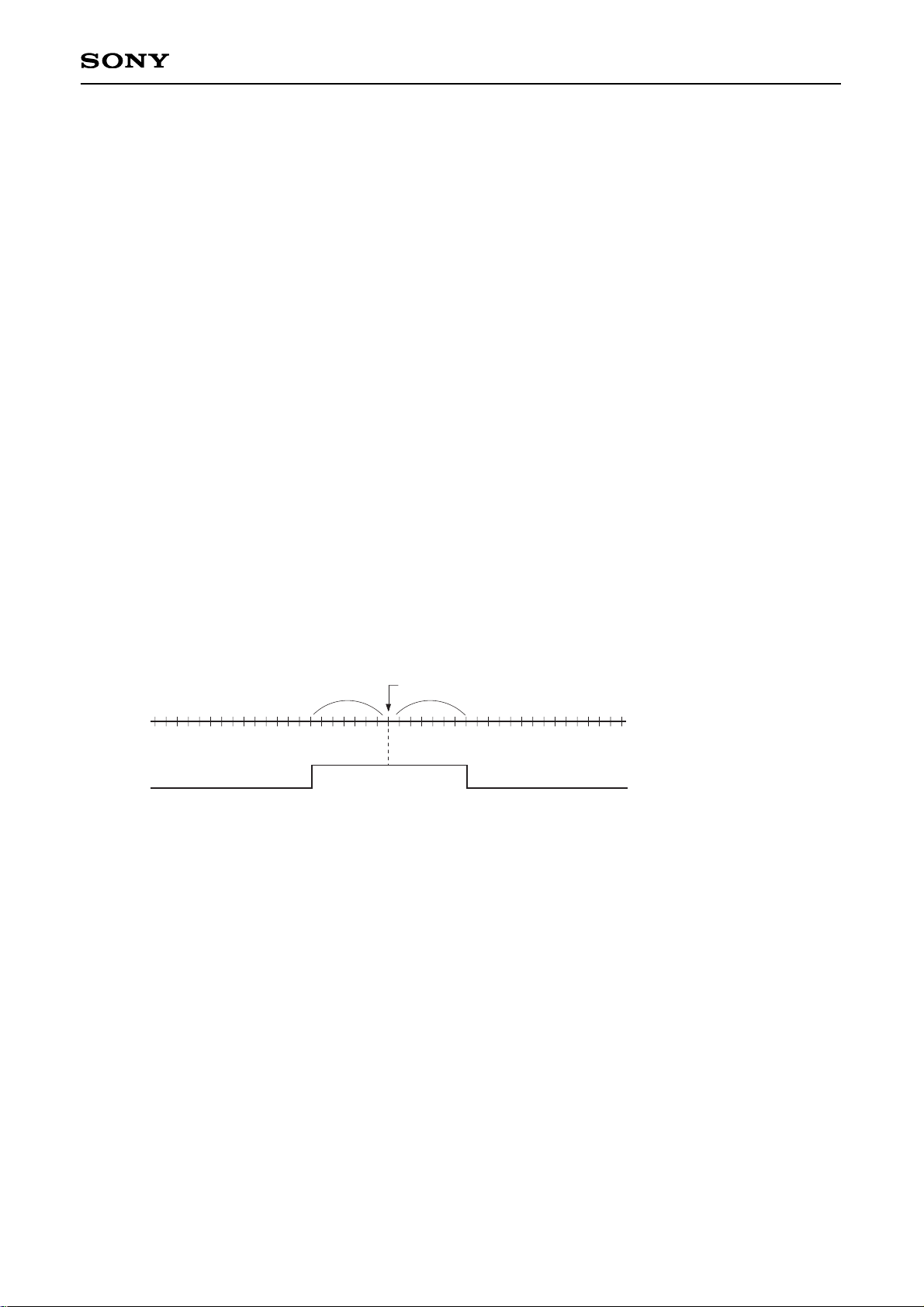
Adjustment Method (Adjust this IC through Tuner and IF when this IC is mounted on the set.)
1.ATT adjustment
1) TEST BIT is set to “TEST1 = 0” and “TEST-DA = 0”.
2) Input a 100Hz, 245mVrms sine wave signal to COMPIN and monitor the LPOUT-L output level. Then,
adjust the “ATT” data for ATT adjustment so that the LPOUT-L output goes to the standard value
(490mVrms).
3) Adjustment range: ±30%
Adjustment bits: 4 bits
2.Stereo, SAPVCO adjustment
1) TEST BIT is set to “TEST1 = 0” and “TEST-DA = 1”.
2) Monitor the LPOUT-R output (4fH free running) frequency in a no input state, and adjust “VCO”
adjustment data so that this frequency is as close to 4fH (62.936kHz) as possible.
3) Adjustment range: ±20%
Adjustment bits: 6 bits
3. Stereo, SAP block, dbx filter adjustment
1) TEST BIT is set to “TEST1 = 1” and “TEST-DA = 0”.
2) Input a 9.4kHz, 600mVrms sine wave signal to COMPIN. While monitoring the STATUS FLAG (STA5)
condition, adjust the “FILTER” adjustment data.
3) Adjustment range: ±20%
Adjustment bits: 6 bits
Align “FILTER” with the center of the STA5 = 1 (adjustment OK) condition range.
4.Separation adjustment
1) TEST BIT is set to “TEST1 = 0” and “TEST-DA = 0”.
2) Set the unit to stereo mode and input the left channel only signal (modulation factor 30%, frequency 300Hz
NR-ON) to COMPIN. At this time, adjust the “WIDEBAND” adjustment data to reduce LPOUT-R output to
the minimum.
3) Next, set the frequency only of the input signal to 3kHz and adjust the “SPECTRAL” adjustment data to
reduce LPOUT-R output to the minimum.
4) The adjustments in 2 and 3 above are performed to optimize the separation.
5) “WIDEBAND” “SPECTRAL”
Adjustment range: ±30% Adjustment range: ±15%
Adjustment bits: 6 bits Adjustment bits: 6 bits
Adjustment point
0
3F
1
Control data
"FILTER"
Measurement data
STA5 "FILADJ"
0
Page 22

– 22 –
CXA2074Q/S
Description of Operation [The pin numbers in parenthesis are for the CXA2074Q.]
The US audio multiplexing system possesses the base band spectrum shown in Fig. 1.
Fig. 1. Base band spectrum
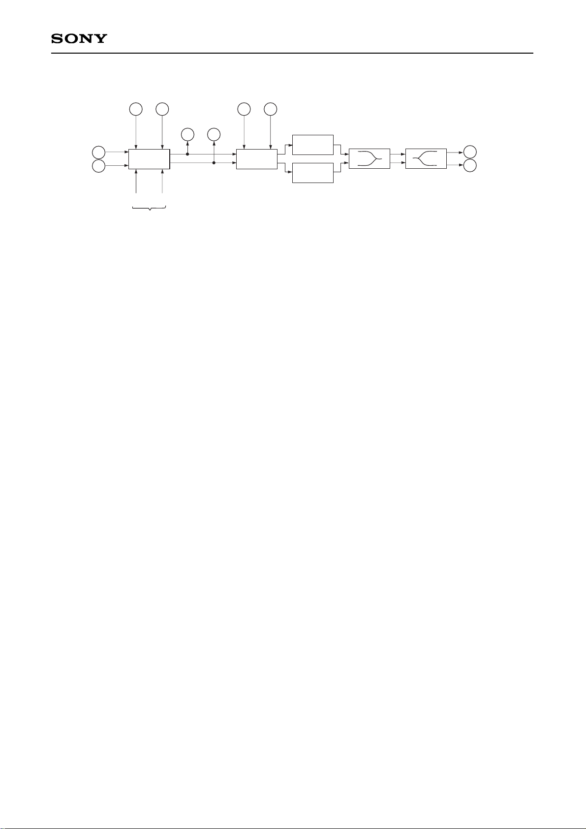
Fig. 2. Overall block diagram (See Fig. 3 for the dbx-TV block)
Fig 3. dbx-TV block
PEAK DEV
kHz
50
25
25
L + R
50 – 15kHz
L-R
dbx-TV
NR
50
AM-DSB-SC
SAP
dbx-TV NR
FM 10kHz
50 – 10kHz
TELEMETRY
FM 3kHz
15
f
H = 15.734kHz
f
H 2fH 3fH 4fH 5fH 6fH 6.5fH
f
5
PILOT
3
(COMPIN)
STEREO LPF
PLL
(VCO 8f
H)
2f
HL0°
f
HL90°
f
HL0°
MODE
CONTROL
PILOT
DET
MVCA
PILOT
CANCEL
MAIN LPF DE.EM
(MAIN OUT)
L + R
4.7µ
(MAIN IN)
L-R (DSB)
DET
INJ.
LOCK
SUBVCA
SUB LPF
WIDEBAND
(SUBOUT)
(ST IN)
4.7µ
NR SW
dbx-TV
BLOCK
MATRIX
(Lch)
(Rch)
MODE
CONTROL
(SAP IN)
4.7µ
SAP(FM)
DET
SAP LPF
MODE
CONTROL
SAP BPF
(SAP OUT)
L – R
to
TVSW
NOISE
DET
I2C BUS
DECODER
SAP
DET
17
13
12
23
24
26
27
A B
I2C BUS
DECODER
I
2
C BUS
DECODER
(14)
(9) (8)
(21) (22)
(25)
(24)
NR SW
FIXED
DEEMPHASIS
VARIABLE
DEEMPHASIS
(VE OUT) (VCA IN)
to
MATRIX
4.7µ
HPF
LPF
LPF
RMS
DET
RMS
DET
VCA
24
27
32
A B
31
(ST IN)
(SAP IN)
(22)
(25)
(30) (31)
Page 23
– 23 –
CXA2074Q/S
Fig. 4. Sound processor block
(1) L + R (MAIN)
After the audio multiplexing signal input from COMPIN (Pin 17 (Pin 14)) passes through MVCA, the
SAP signal and telemetry signal are suppressed by STEREO LPF. Next, the pilot signals are
canceled. Finally, the L – R signal and SAP signal are removed by MAIN LPF, and frequency
characteristics are flattened (de-emphasized) and input to the matrix.
(2) L – R (SUB)
The L – R signal follows the same course as L + R before the pilot signal is canceled. L – R has no
carrier signal, as it is a suppressed-carrier double-sideband amplitude modulated signal (DSB-AM
modulated). For this reason, the pilot signal is used to regenerate the carrier signal (quasi-sine wave)
to be used for the demodulation of the L – R signal. In the last stage, the residual high frequency
components are removed by SUB LPF and the L – R signal is input to the dbx-TV block via the NRSW
circuit after passing through SUBVCA.
(3) SAP
SAP is an FM signal using 5fH as a carrier as shown in the Fig. 1. First, the SAP signal only is
extracted using SAP BPF. Then, this is subjected to FM detection. Finally, residual high frequency
components are removed and frequency characteristics flattened using SAP LPF, and the SAP signal
is input to the dbx-TV block via the NRSW circuit. When there is no SAP signal, the Pin 26 output is
soft muted.
(4) Mode discrimination
Stereo discrimination is performed by detecting the pilot signal amplitude. SAP discrimination is
performed by detecting the 5fH carrier amplitude. NOISE discrimination is performed by detecting the
noise near 25kHz after FM detection of SAP signal.
(5) dbx-TV block
Either the L – R signal or SAP signal input respectively from ST IN (Pin 24 (Pin 22)) or SAP IN (Pin 27
(Pin 25)) is selected by the mode control and input to the dbx-TV block.
The input signal then passes through the fixed de-emphasis circuit and is applied to the variable deemphasis circuit. The signal output from the variable de-emphasis circuit passes through an external
capacitor and is applied to VCA (voltage control amplifier). Finally, the VCA output is converted from a
current to a voltage using an operational amplifier and then input to the matrix.
(Lch) (Rch)
(AUX1-L)
(AUX1-R)
from MATRIX
(LPIN-L)
PASSSW
BASS
TREBLE
(LSOUT-L)
(LSOUT-R)
40
39
41
42
(LPIN-R)
(LPOUT-L) (LPOUT-R)
TVSW
(AUX2-L) (AUX2-R)
37
38
36
35
VOL-L
VOL-R
7
8
(3)
(2)
Page 24
– 24 –
CXA2074Q/S
The variable de-emphasis circuit transmittance and VCA gain are respectively controlled by Each of
effective value detection circuits. Each of the effective value detection circuits passes the input signal
through a predetermined filter for weighting before the effective value of the weighted signal is
detected to provide the control signal.
(6) Matrix, TVSW, PASSSW
The signals (L + R, L – R, SAP) input to “MATRIX” become the outputs for the ST-L, ST-R, MONO and
SAP signals according to the BUS data and whether there is ST / SAP discrimination.
“TVSW” switches the “MATRIX” output signal, external input signal (input to AUX1-L, R), external input
signal (input to AUX2-L, R) and external forced MONO.
“PASSSW” switches the “TVSW” output signal and external input signal (input to LPIN-L, R).
(7) Sound processor block
The sound processor block contains, “BASS/TREBLE” tone control functions, and “VOLUME”.
BASS: ±12dB (±1.7dB/STEP at 100Hz)
TREBLE: ±12dB (±1.7dB/STEP at 10kHz)
VOLUME: 0 to –80dB (–1.25dB/STEP)
(8) Others
“MVCA” is a VCA which adjusts the input signal level to the standard level of this IC.
“Bias” supplies the reference voltage and reference current to the other blocks. The current flowing to
the resistor connecting IREF (Pin 19 (Pin 16)) with GND become the reference current.
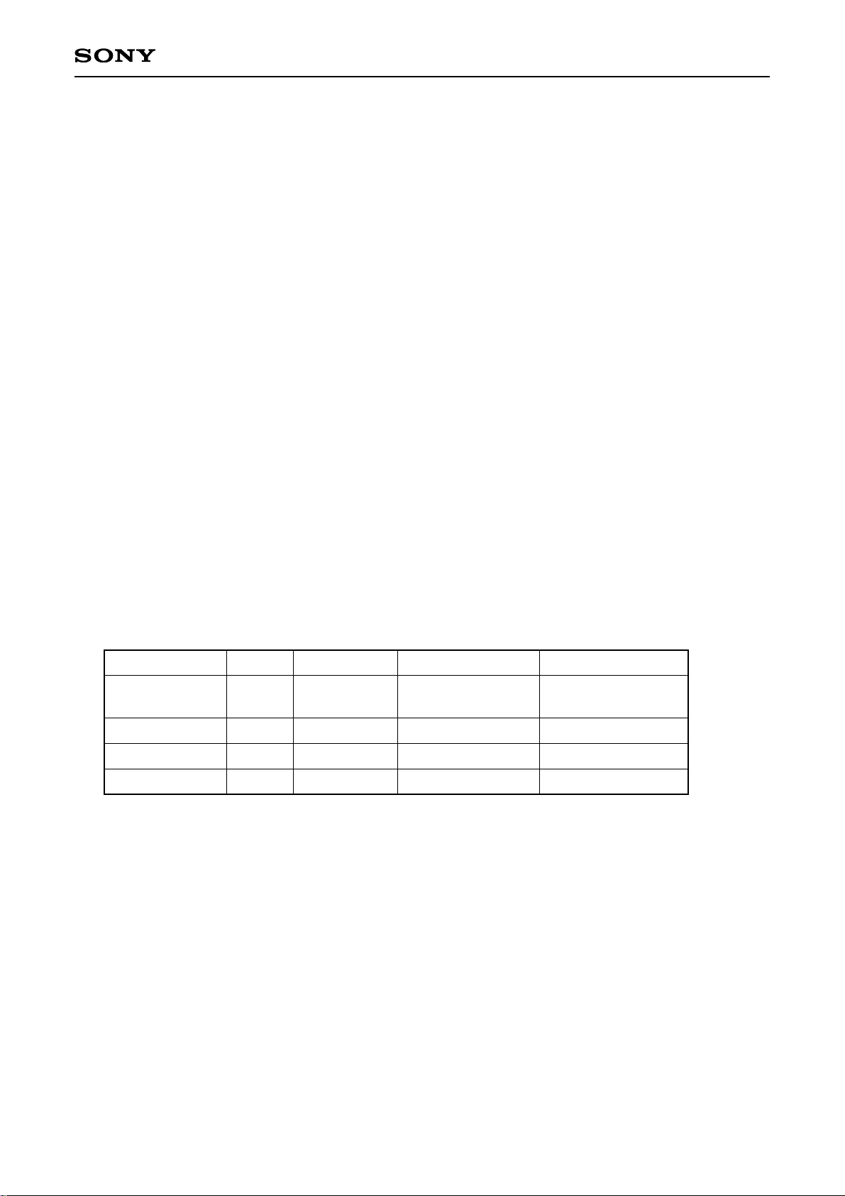
Standard input and output levels
490mVrms
∗2
490mVrms
490mVrms
490mVrms
17
(14)
36/35
38/37
42/41
245mVrms
∗1
490mVrms
490mVrms
490mVrms
490mVrms
∗2
490mVrms
490mVrms
—
Input pin Pin No.
Input level LPOUT output level
LSOUT output level
∗3
COMPIN
AUX1-L/AUX1-R
AUX2-L/AUX2-R
LPIN-L/LPIN-R
∗1
MONO, 25kHz Deviation, Pre-Em. off
∗2
MONO, 25kHz Deviation, Pre-Em. on
∗3
VOLUME MAX, BASS & TREBLE CENTER
Page 25

– 25 –
CXA2074Q/S
VCO (6)
FILTER (6)
SPECTRAL (6)
WIDEBAND (6)
VOL-L (6)
VOL-R (6)
∗∗∗∗0000
∗∗∗∗0001
∗∗∗∗0010
∗∗∗∗0011
∗∗∗∗0100
∗∗∗∗0101
∗∗∗∗0110
∗∗∗∗0111
∗∗∗∗1000
∗∗∗∗1001
∗∗∗∗1010
∗
∗
∗
∗
∗
∗
∗
∗
∗
∗
∗
SLAVE RECEIVER
80H (1000 0000)
SLAVE TRANSMITTER
81H (1000 0001)
Register Specifications
Slave address
Register table
when TEST1 = 0
Status Registers
DATA
SUB ADDRESS
MSB LSB
BIT7 BIT6 BIT5 BIT4 BIT3 BIT2 BIT1 BIT0
TEST-DA
ATTSW
PSW
TEST1
FST
FEXT1
NRSW
FEXT2
FOMO
TVSW
SAPC
EXT
M1
M2
BASS (4)
TREBLE (4)
when TEST1 = 1
STA1
BIT7
POWER
ON RESET
STA2
BIT6
STEREO
STA3
BIT5
SAP
STA4
BIT4
NOISE
STA5
BIT3
—
STA6
BIT2
—
STA7
BIT1
—
STA8
BIT0
—
STA1
BIT7
POWER
ON RESET
STA2
BIT6
STEREO
STA3
BIT5
SAP
STA4
BIT4
NOISE
STA5
BIT3
FILADJ
STA6
BIT2
—
STA7
BIT1
—
STA8
BIT0
—
ATT (4)
∗: Don't Care
Page 26
– 26 –
CXA2074Q/S
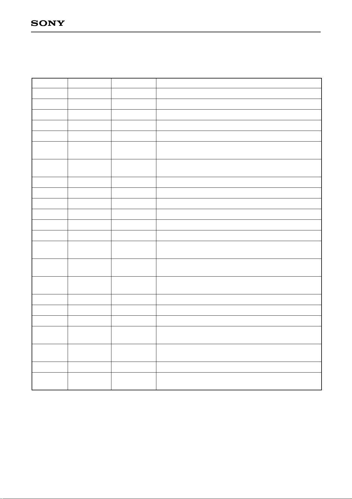
Description of Registers
Control registers
∗1
Classification U: User control
A: Adjustment
S: Proper to set
T: Test
ATT
VCO
FILTER
SPECTRAL
WIDEBAND
TEST-DA
TEST1
FST
VOL-L
VOL-R
BASS
TREBLE
NRSW
FOMO
TVSW
EXT
FEXT1
FEXT2
PSW
M1
M2
ATTSW
SAPC
4
6
6
6
6
1
1
1
6
6
4
4
1
1
1
1
1
1
1
1
1
1
1
A
A
A
A
A
T
T
T
U
U
U
U
U
U
U
U
U
U
U
U
U
S
S
Input level adjustment
STEREO VCO & SAP VCO free running frequency adjustment
STEREO and SAP and dbx filter adjustment
Adjustment of stereo separation (3kHz)
Adjustment of stereo separation (300Hz)
Turn to DAC test mode and VCO adjustment mode by means
of TEST-DA = 1.
Turn to test mode by means of TEST = 1.
(Adjustment of FILTER)
Turn to forced stereo by means of FST = 1.
LSOUT-L output signal level control
LSOUT-R output signal level control
LSOUT output bass control
LSOUT output treble control
Selection of the output signal (Stereo mode, SAP mode)
Turn to forced MONO by means of FOMO = 1.
(Left channel only is MONO during SAP output.)
Selection of TV mode or external input mode for LPOUT
output
Selection of external input 1 mode or external input 2 mode
for LPOUT output. (TVSW = 1)
External input 1 forced MONO (1: forced MONO ON)
External input 2 forced MONO (1: forced MONO ON)
Selection of internal mode or LPIN mode for LSOUT output.
Selection of LPOUT mute ON/OFF
(0: mute ON, 1: mute OFF)
Selection of LSOUT mute ON/OFF
(0: mute ON, 1: mute OFF)
Turn the input stage MVCA off when ATTSW = 1.
Selection of SAP mode or L + R mode according to the
presence of SAP broadcasting
Register
Number of bits
Classification
∗1
Contents
Page 27
– 27 –
CXA2074Q/S
Status registers
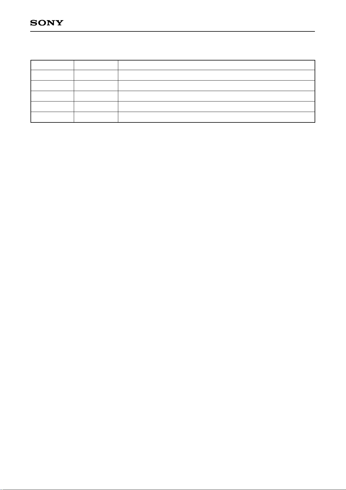
Description of Control Registers
ATT (4): Adjust the signal level input to COMPIN (Pin 17 (Pin 14)) to the standard input level (245mVrms).
Variable range of the input signal: 245mVrms –5.0dB to +3.0dB
0 = Level min.
F = Level max.
VCO (6): Adjust STEREO & SAP VCO free running frequency (fo).
Variable range: fo ±20%
0 = Free running frequency min.
3F = Free running frequency max.
FILTER (6): Adjust the filter fo of the ST, SAP and dbx blocks.
Variable range: fo ±20%
0 = Frequency min.
3F= Frequency max.
SPECTRAL (6): Perform high frequency (fs = 3kHz) separation adjustment.
0 = Level max.
3F = Level min.
WIDEBAND (6):Perform low frequency (fs = 300Hz) separation adjustment.
0 = Level min.
3F = Level max.
TEST-DA (1):Set DAC output test mode and VCO adjustment mode.
0 = Normal mode
1 = DAC output test mode and VCO adjustment mode
In addition, the following outputs are present at Pins 40 and 39.
LPOUT-L (Pin 40): DA control DC level
LPOUT-R (Pin 39): STEREO VCO oscillation frequency (4fH)
PONRES
STEREO
SAP
NOISE
FILADJ
1
1
1
1
1
POWER ON RESET detection; 1: RESET
Stereo discrimination of the COMPIN input signal; 1: Stereo
SAP discrimination of the COMPIN input signal; 1: SAP
Noise level discrimination of the SAP signal; 1: Noise
Status of FILTER adjustment; 1: OK range
Register Number of bits Contents
Page 28

– 28 –
CXA2074Q/S
TEST1 (1): Set filter adjustment mode.
0 = Normal mode
1 = FILTER (STA5) adjustment mode
In addition, the following outputs are present at Pins 40 and 39.
LPOUT-L (Pin 40): SAP BPF OUT
LPOUT-R (Pin 39): NR BPF OUT
FST (1): Select forced STEREO mode
0 = Normal mode
1 = Forced stereo mode
VOL-L (6): LSOUT-L output signal level control
0 = Volume Min. (–80dB)
3F= Volume Max. (0dB)
–1.25 dB/STEP
VOL-R (6): LSOUT-R output signal level control
0 = Volume Min. (–80dB)
3F= Volume Max. (0dB)
–1.25 dB/STEP
BASS (4): LSOUT output bass control
0 = Bass Min.
7 & 8 = Bass Center (0dB)
F = Bass Max.
TREBLE (4): LSOUT output treble control
0 = Treble Min.
7 & 8 = Treble Center (0dB)
F = Treble Max.
NRSW (1): Select stereo mode or SAP mode
0 = Stereo mode
1 = SAP mode
FOMO (1): Select forced MONO mode
0 = Normal mode
1 = Forced MONO mode
TVSW (1): Select TV mode or external input mode for LPOUT output.
0 = TV mode
1 = External input mode
EXT (1): Select external input [1] mode or external input [2] mode for LPOUT output. (TVSW = 1)
0 = External input [1] mode
1 = External input [2] mode
Page 29

– 29 –
CXA2074Q/S
FEXT1 (1): Turn external input [1] to forced MONO.
0 = Normal mode
1 = External input [1] is forced MONO.
Input the same signal to both AUX1-L and AUX1-R.
FEXT2 (1): Turn external input [2] to forced MONO
0 = Normal mode
1 = External input [2] is forced MONO
Input the same signal to both AUX2-L and AUX2-R.
PSW (1) Select INT mode or LPIN mode for LSOUT output.
0 = INT mode
1 = LPIN mode
M1 (1): Mute the LPOUT-L and LPOUT-R output.
0 = Mute ON
1 = Mute OFF
M2 (1): Mute the LSOUT-L and LSOUT-R output.
0 = Mute ON
1 = Mute OFF
ATTSW (1) Select BYPASS SW of MVCA
0 = Normal mode
1 = MVCA is passed
SAPC (1): Select the SAP signal output mode
When there is no SAP signal, the conditions for selecting SAP output are selected by
SAPC.
0 = L + R output is selected
1 = SAP output is selected
Page 30

– 30 –
CXA2074Q/S
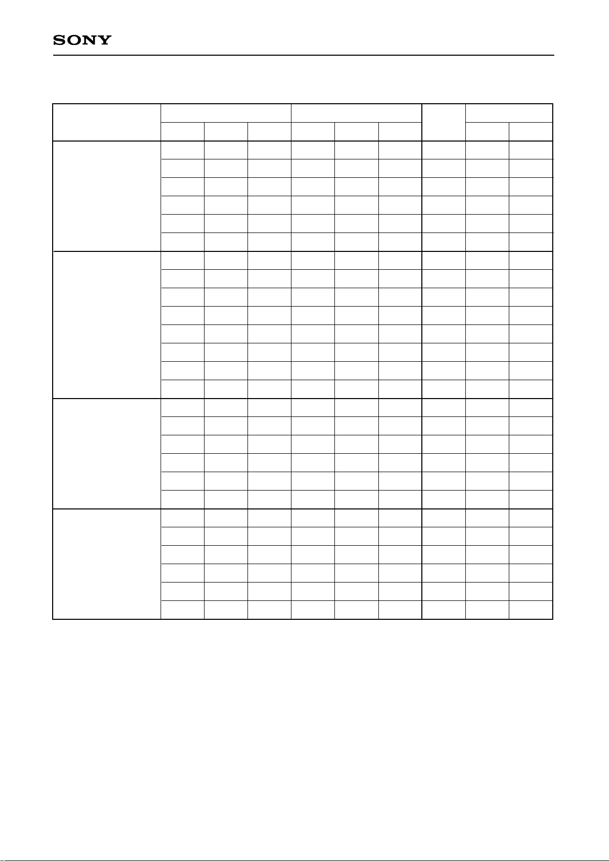
Description of Mode Control
Priority ranking: M1/M2 > TVSW/EXT > TEST-DA > TEST1 > (NRSW & FOMO & SAPC)
NRSW
FOMO
SAPC
M1/M2
TVSW/EXT
TEST1
TEST-DA
“Select dbx input and TV decoder output”
Conditions: FOMO = 0
NRSW = 0 (MONO or ST output)
• During ST input: left channel: L,
right channel: R
• During other input: left channel: L + R,
right channel: L + R
NRSW = 1 (SAP output)
• When there is “SAP” during SAP
discrimination
– left channel: SAP, right channel: SAP
• When there is “No SAP”, output is the
same as when NRSW = 0.
“Select dbx input and TV decoder output”
Conditions: FOMO = 0
NRSW = 0 (MONO or ST output)
As on the left
NRSW = 1 (SAP output)
• Regardless of the presence of SAP
discrimination,
dbx input: “SAP”
left channel: SAP, right channel: SAP
However, when there is no SAP, SAPOUT
output is soft muted (–7dB)
Mode control SAPC = 0 SAPC = 1
“Forced MONO”
FOMO = 1
• During SAP output: left channel: L + R, right channel: SAP
• During ST or MONO output: left channel: L + R, right channel: L + R
Change the selection conditions for “MONO or ST output” and “SAP output”.
SAPC = 0: Switch to SAP output when there is SAP discrimination.
Do not switch to SAP output when there is no SAP discrimination.
SAPC = 1: Switch to SAP output regardless of whether there is SAP discrimination.
“MUTE”
M1 = 0: LPOUT output is muted.
M2 = 0: LSOUT output is muted.
“TV mode/external input mode selection”
TVSW = 0: Set LPOUT output to TV mode.
TVSW = 1: Set LPOUT output to external input mode.
EXT = 0: Set LPOUT output to external input [1] mode. (TVSW = 1)
EXT = 1: Set LPOUT output to external input [2] mode. (TVSW = 1)
“TEST1”
TEST1 = 1
Return adjustment data with STATUS REGISTER as an adjustment mode.
In addition, outputs are as follows.
left channel: SAP BPF OUT
right channel: NR BPF OUT
“TEST-DA”
TEST-DA = 1
Used to adjust the D/A TEST and VCO.
left channel: D/A output
right channel: STVCO oscillation frequency (4fH)
Page 31
– 31 –
CXA2074Q/S
Decoder Output and Mode Control Table 1 (SAPC = 1)
Note
(SAP) : The SAPOUT output signal is soft muted (approximately –7dB).
The signal is soft muted when NOISE = 1.
∗ : Don’t care.
∗1
SAP or NOISE discrimination may be made during MONO or STEREO input when the noise is
inputted in the weak electric field.
"NOISE" status rises earlier than "SAP" status when the amount of noise is increased to COMPIN.
0 0 0 0 ∗ 1 MUTE L + R L + R
0 0 0 1 0 1 SAP SAP SAP
MONO
0 0 0 1 1 1 SAP L + R SAP
0 ∗ 1 0 ∗ 1 MUTE L + R L + R
0 ∗ 1 1 0 1 (SAP) (SAP) (SAP)
0 ∗ 1 1 1 1 (SAP) L + R (SAP)
1 0 ∗ 0 0 1 L – R L R
1 0 ∗ 0 1 1 MUTE L + R L + R
1 1 1 0 0 1 L – R L R
STEREO
1 1 1 0 1 1 MUTE L + R L + R
1 0 0 1 0 1 SAP SAP SAP
1 0 0 1 1 1 SAP L + R SAP
1 ∗ 1 1 0 1 (SAP) (SAP) (SAP)
1 ∗ 1 1 1 1 (SAP) L + R (SAP)
0 1 ∗ 0 0 1 MUTE L + R L + R
0 1 ∗ 0 1 1 MUTE L + R L + R
MONO & SAP
0 1 0 1 0 1 SAP SAP SAP
0 1 0 1 1 1 SAP L + R SAP
0 1 1 1 0 1 (SAP) (SAP) (SAP)
0 1 1 1 1 1 (SAP) L + R (SAP)
1 1 ∗ 0 0 1 L – R L R
1 1 ∗ 0 1 1 MUTE L + R L + R
STEREO & SAP
1 1 0 1 0 1 SAP SAP SAP
1 1 0 1 1 1 SAP L + R SAP
1 1 1 1 0 1 (SAP) (SAP) (SAP)
1 1 1 1 1 1 (SAP) L + R (SAP)
Input signal mode
Mode detection
Mode control
dbx
input
Output
ST SAP NOISE NRSW FOMO SAPC Lch Rch
∗1
∗1
Page 32
– 32 –
CXA2074Q/S
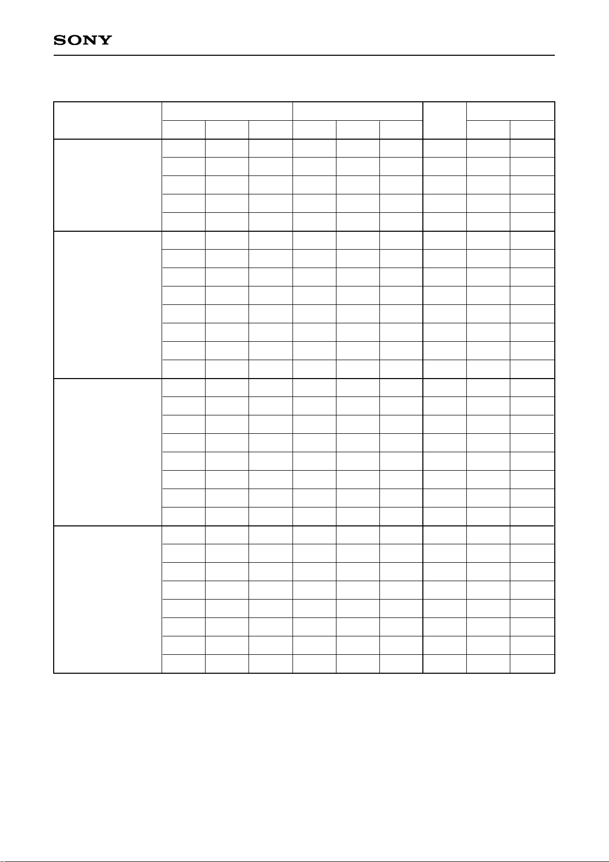
Decoder Output and Mode Control Table 2 (SAPC = 0)
Note
(SAP) : The SAPOUT output signal is soft muted (approximately –7dB).
The signal is soft muted when NOISE = 1.
∗ : Don’t care.
∗1
SAP or NOISE discrimination may be made during MONO or STEREO input when the noise is
inputted in the weak electric field.
"NOISE" status rises earlier than "SAP" status when the amount of noise is increased to COMPIN.
0 0 ∗ ∗ ∗ 0 MUTE L + R L + R
0 1 1 0 0 0 MUTE L + R L + R
MONO 0 1 1 0 1 0 MUTE L + R L + R
0 1 1 1 0 0 (SAP) (SAP) (SAP)
0 1 1 1 1 0 (SAP) L + R (SAP)
1 0 ∗ 0 0 0 L – R L R
1 0 ∗ 0 1 0 MUTE L + R L + R
1 0 ∗ 1 0 0 L – R L R
STEREO
1 0 ∗ 1 1 0 MUTE L + R L + R
1 1 1 0 0 0 L – R L R
1 1 1 0 1 0 MUTE L + R L + R
1 1 1 1 0 0 (SAP) (SAP) (SAP)
1 1 1 1 1 0 (SAP) L + R (SAP)
0 1 0 0 0 0 MUTE L + R L + R
0 1 0 0 1 0 MUTE L + R L + R
0 1 0 1 0 0 SAP SAP SAP
MONO & SAP
0 1 0 1 1 0 SAP L + R SAP
0 1 1 0 0 0 MUTE L + R L + R
0 1 1 0 1 0 MUTE L + R L + R
0 1 1 1 0 0 (SAP) (SAP) (SAP)
0 1 1 1 1 0 (SAP) L + R (SAP)
1 1 0 0 0 0 L – R L R
1 1 0 0 1 0 MUTE L + R L + R
1 1 0 1 0 0 SAP SAP SAP
STEREO & SAP
1 1 0 1 1 0 SAP L + R SAP
1 1 1 0 0 0 L – R L R
1 1 1 0 1 0 MUTE L + R L + R
1 1 1 1 0 0 (SAP) (SAP) (SAP)
1 1 1 1 1 0 (SAP) L + R (SAP)
Input signal mode
Mode detection
Mode control
dbx
input
Output
ST SAP NOISE NRSW FOMO SAPC Lch Rch
∗1
∗1
Page 33
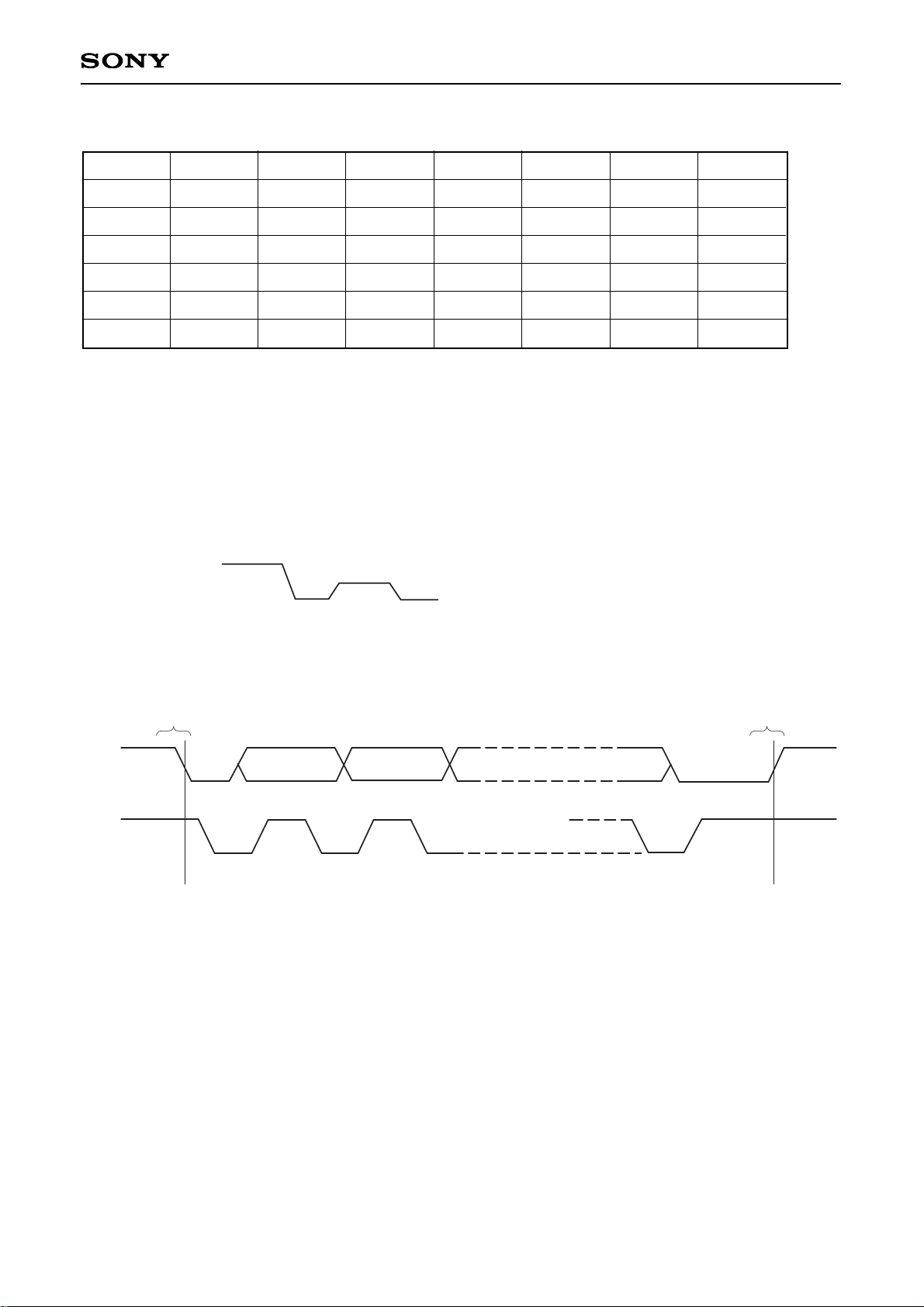
Mode Control Table 3
TV (L) / TV (R) are selected in MATRIX
TV (L): MONO, ST-L, SAP, (SAPBPFout, D/Aout)
TV (R): MONO, ST-R, SAP, (NRBPFout, STVCO freerun (4fH))
I2C BUS Signal
There are two I2C signals, SDA (Serial DATA) and SCL (Serial CLOCK) signals. SDA is a bidirectional signal.
• Accordingly there are 3 values outputs, H, L and HIZ.
• I2C transfer begins with Start Condition and ends with Stop Condition.
– 33 –
CXA2074Q/S
TVSW
–
0
1
1
1
1
SDA
SCL
Start Condition S Stop Condition P
FEXT2
–
–
–
–
0
1
FEXT1
–
–
0
1
–
–
EXT
–
–
0
0
1
1
M1
0
1
1
1
1
1
1
2
3
4
5
6
LPOUT-L
MUTE
TV (L)
AUX1-L
AUX1-L
AUX2-L
AUX2-L
LPOUT-R
MUTE
TV (R)
AUX1-R
AUX1-L
AUX2-R
AUX2-L
H L HIZ L
Page 34
– 34 –
CXA2074Q/S
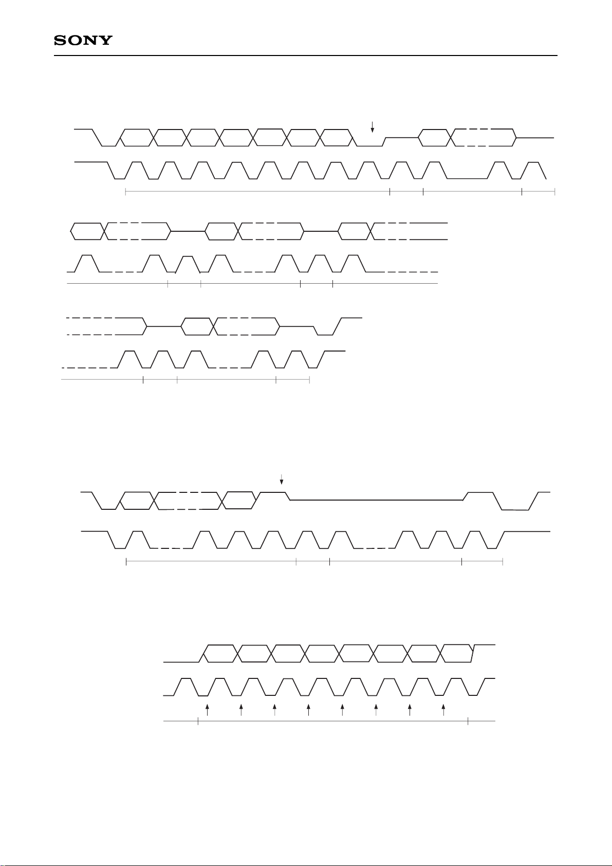
• I2C data Write (Write from I2C controller to the IC)
∗
Data can be transferred in 8-bit units to be
set as required.
Sub address is incremented automatically.
• I2C data Read (Read from the IC to I2C controller)
• Read timing
∗
Data Read is performed during SCL rise.
S
Address
1 6 7 8 9 1 8 9
SCL
ACK DATA ACK
SDA
H during Read
HIZ
7
P
DATA
1 2 3 4 5 6 7 89 9
IC output SDA
SCL
MSB
LSB
ACK ACK
Read timing
ACKACKDATA DATA
P
8 9 1 8 9
HIZ HIZ
DATA (n) DATA (n + 1)ACK
1 8
9
1 8 9
ACK DATA (n + 2)
HIZ HIZ
LSBMSB
S
Address
1 2 3 4 5 6 7 8 9 1 8 9
SDA
SCL
MSB
L during Write
MSB LSB
HIZ HIZ
ACK Sub Address ACK
Page 35
– 35 –
CXA2074Q/S
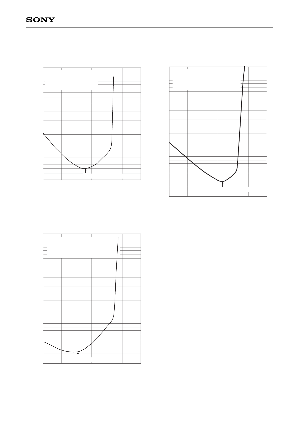
Input level vs. Distortion characteristics 1 (MONO)
Distortion [%]
1.0
0.1
–10 0 10
Input level vs. Distortion characteristics 2 (Stereo)
Distortion [%]
10
1.0
–10 0 10
Input level [dB]
Input signal: Stereo L = –R
(dbx-TVNR ON), 1kHz
0dB = 100% modulation level
V
CC = 9V, 30kHz using LPF, ST mode
Measurement point: LPOUT-L/R
Input level vs. Distortion characteristics 3 (SAP)
Distortion [%]
10
1.0
–10 0 10
Input level [dB]
Input level [dB]
Standard level (100%)
Standard level (100%)
Input signal: SAP (dbx-TVNR ON)
1kHz, 0dB = 100% modulation
level
V
CC = 9V, 30kHz using LPF, SAP mode
Measurement point: LPOUT-L/R
Standard level (100%)
Input signal: MONO (Pre-emphasis on), 1kHz
0dB = 100% modulation level
V
CC = 9V, 30kHz using LPF
Measurement point: LPOUT-L/R
Page 36
– 36 –
CXA2074Q/S
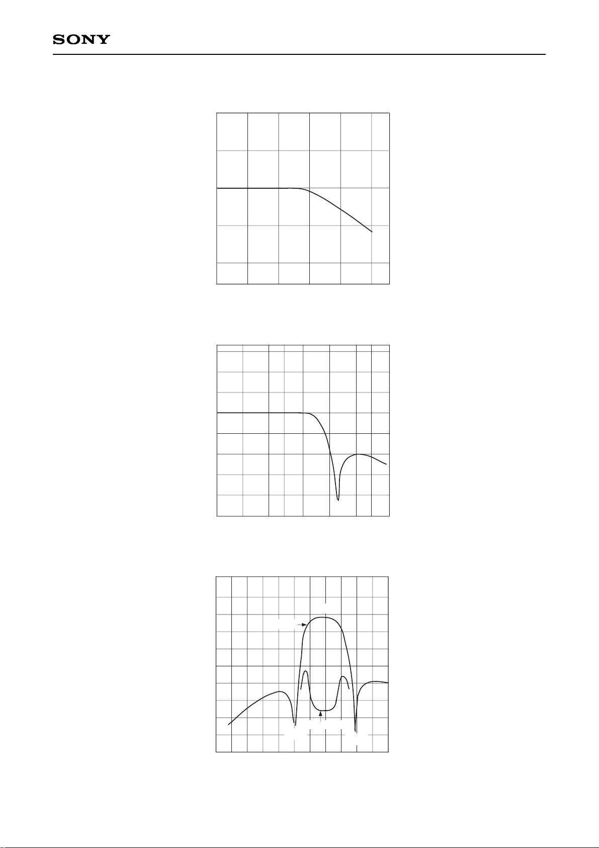
Frequency [kHz]
Gain [dB]
Stereo LPF frequency characteristics
10
5
0
–5
–10
0 20 40 60 80 100
30
10
0
–20
–50
1 2 5 10 20 507 70 100
–40
–30
–10
20
Gain (FC main and FC sub) [dB]
10
0
–20
20 40 60 80 100 120
–10
20
SAP frequency characteristics and group delay
Group delay [µs]
100
90
80
70
60
50
40
10
20
0
30
5fH
Gain
Group delay
3.8fH
6.2fH
Frequency [kHz]
Frequency [kHz]
Main LPF and Sub LPF frequency characteristics
Gain [dB]
Page 37
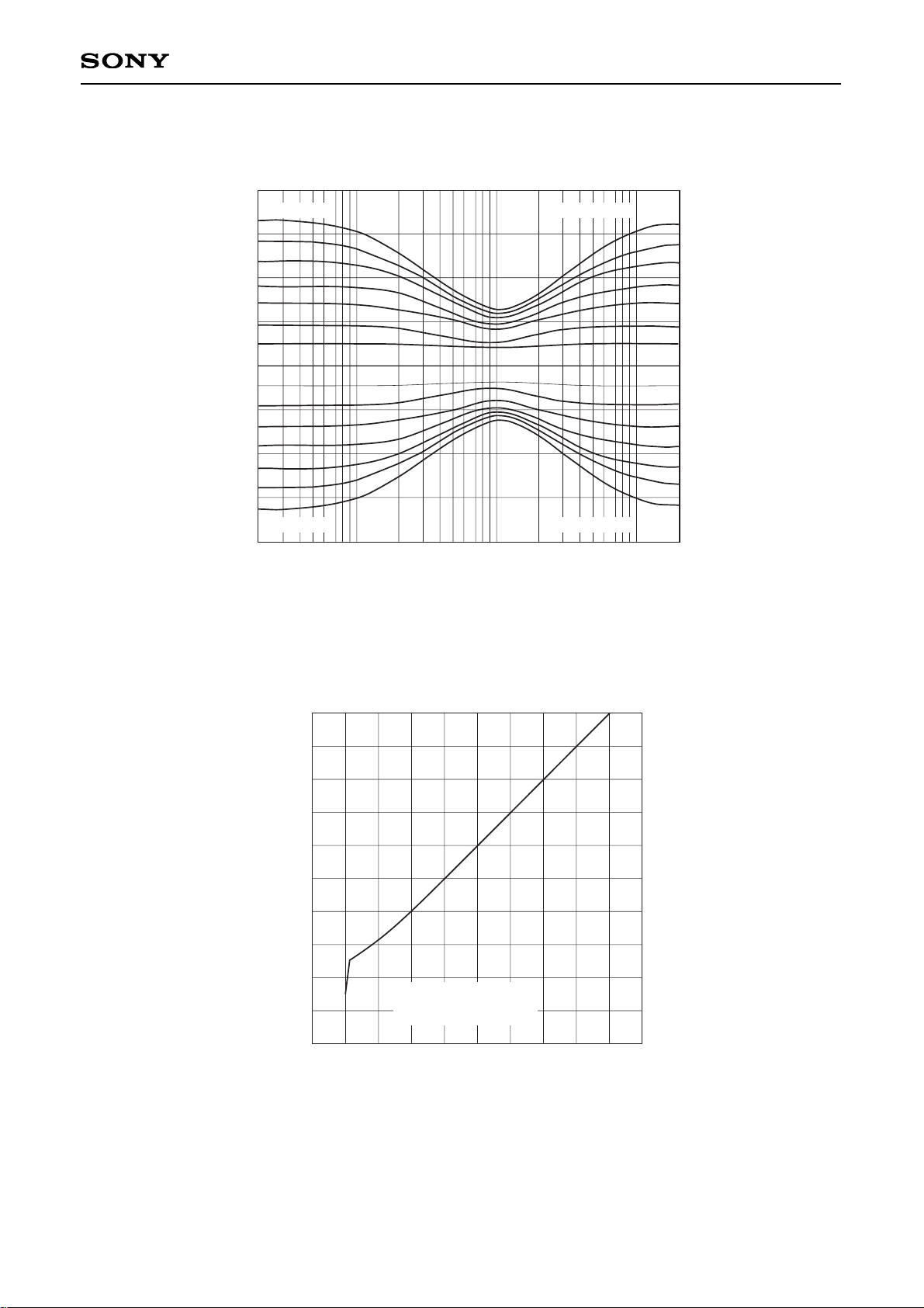
– 37 –
CXA2074Q/S
20 100 1k
Frequency [Hz]
10k 20k
Input: AUX1, 2
245mVrms
Output: LSOUT
TREBLE. MINBASS. MIN
BASS. MAX TREBLE. MAX
+12
+8
+4
0
–4
–8
–12
Boost amount [dB]
BASS-TREBLE characteristics
0 F 1F
Control data VOL-L, VOL-R
2F 3F
Input: AUX1, 2
1kHz, 490mVrms
Output: LSOUT
0
–20
–40
–60
–80
–100
LSOUT output level [dB]
Volume characteristics
Page 38
– 38 –
CXA2074Q/S
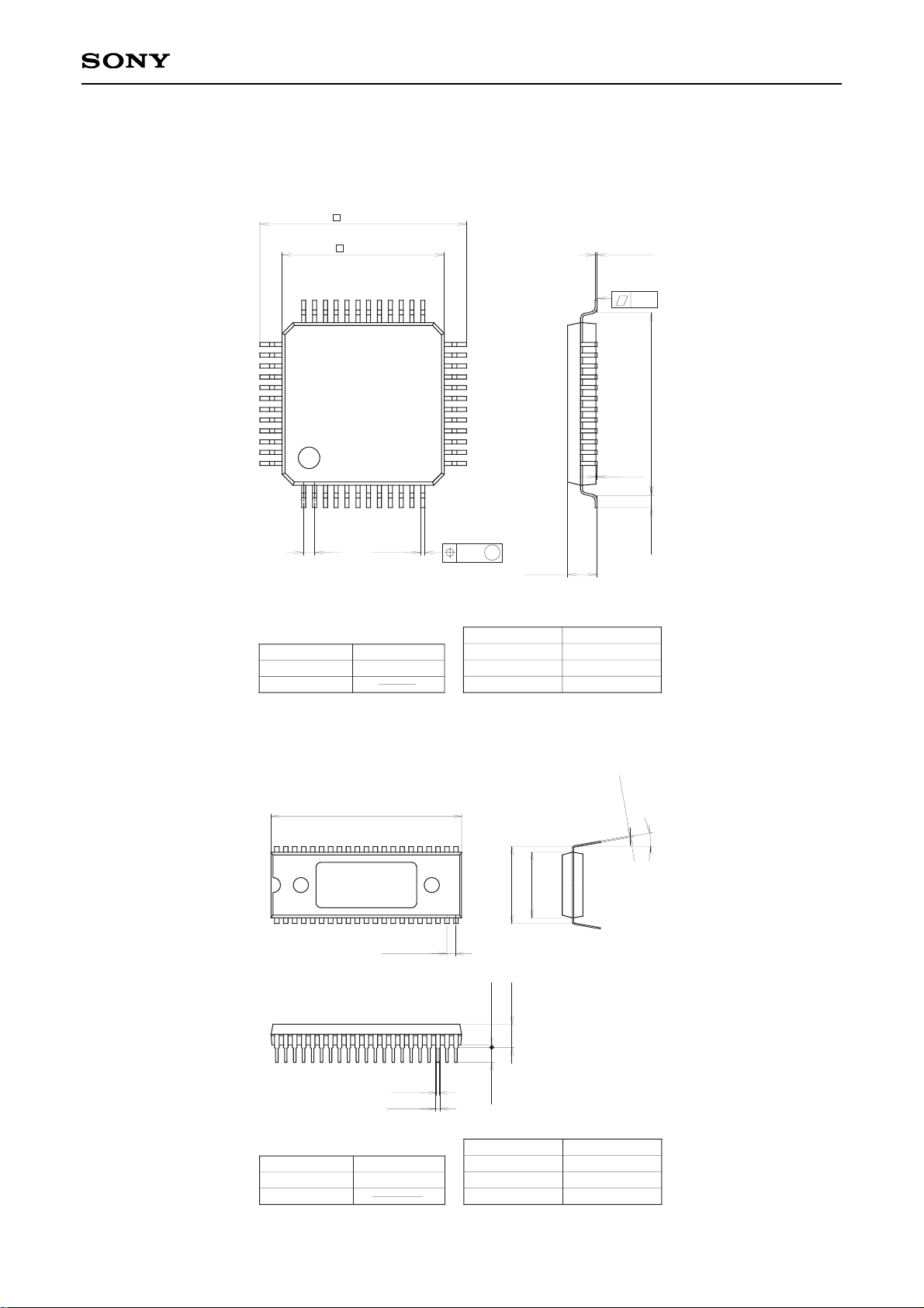
Package Outline Unit: mm
CXA2074Q
42PIN SDIP (PLASTIC) 600mil
37.8
+ 0.4
– 0.1
13.0
+ 0.3
– 0.1
0.25
+ 0.1
– 0.05
42
22
1
21
1.778 ± 0.25
15.24 ± 0.25
0° to 15°
4.6
+ 0.4
– 0.1
0.5 ± 0.1
0.9 ± 0.15
3.0 MIN
0.5 MIN
SONY CODE
EIAJ CODE
JEDEC CODE
PACKAGE STRUCTURE
PACKAGE MATERIAL
LEAD TREATMENT
LEAD MATERIAL
PACKAGE WEIGHT
EPOXY RESIN
SOLDER PLATING
COPPER / 42 ALLOY
SDIP-42P-02
SDIP042-P-0600-A
4.4g
SONY CODE
EIAJ CODE
JEDEC CODE
M
PACKAGE STRUCTURE
PACKAGE MATERIAL
LEAD TREATMENT
LEAD MATERIAL
PACKAGE WEIGHT
EPOXY RESIN
SOLDER / PALLADIUM
PLATING
COPPER / 42 ALLOY
48PIN QFP (PLASTIC)
15.3 ± 0.4
12.0 – 0.1
+ 0.4
0.8 0.3 – 0.1
+ 0.15
± 0.12
13
24
2536
37
48
1 12
2.2 – 0.15
+ 0.35
0.9 ± 0.2
0.1 – 0.1
+ 0.2
13.5
0.15
0.15 – 0.05
+ 0.1
QFP-48P-L04
∗QFP048-P-1212-B
0.7g
CXA2074S
 Loading...