

Page 1
– 1 –
CXA2022S
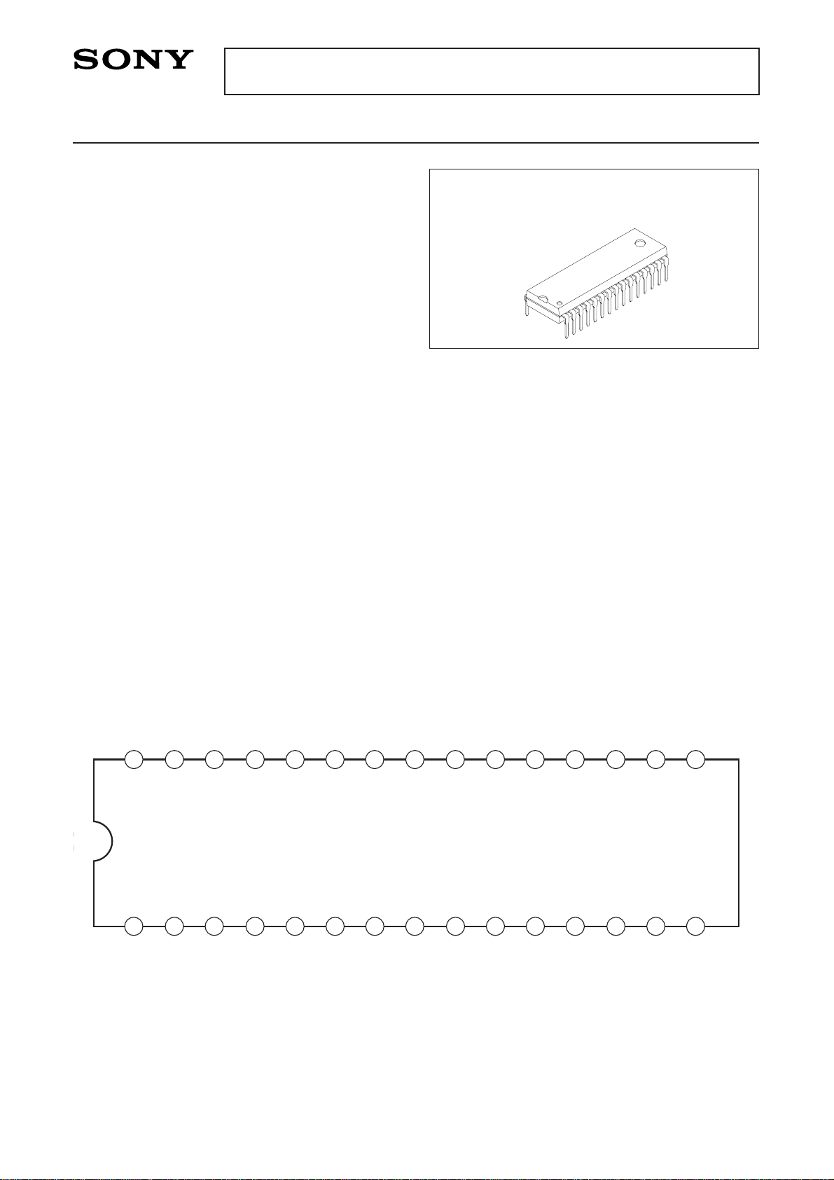
30 pin SDIP (Plastic)
E95Y17A7X
I2C Bus Sound Processor for TV
Description
The CXA2022S is a bipolar IC designed as an I2C
bus control sound processor for TV. This IC has
simulate stereo, surround, tone control, balance,
volume, muting, AGC and other functions.
Features
• Allows control by I2C bus
• Employs a special surround system to prevent
"vocal missing" in the surround mode
• Adopts an AGC circuit to absorb the difference in
sound level between input sources and improves
S/N ratio of hearing characteristics
Absolute Maximum Ratings
• Supply voltage VCC 14 V
• Operating temperature Topr –20 to +75 °C
• Storage temperature Tstg –65 to +150 °C
• Allowable power dissipation PD 1.25 W
Recommended Operating Condition
Supply voltage 8 to 13 V
Pin Configuration
Structure
Bipolar silicon monolithic IC
Applications
TVs
V
CC
CH L
VRS
MVFO
MVFI
PS3B
CC L
LOUT
PS3A
PS1B
PS2B
PS2A
DET1
R IN
GND
CL R
CH R
BAL
TRE
BASS
VOL
CC R
ROUT
PS1A
DET2
HPF
SCL
SDA
L IN
CL L
2
3
4
5
6
7
8
9
10
11
12
13
14 15
1
26
27
28
29
30
16
17
18
19
20
21
22
23
24
25
Sony reserves the right to change products and specifications without prior notice. This information does not convey any license by
any implication or otherwise under any patents or other right. Application circuits shown, if any, are typical examples illustrating the
operation of the devices. Sony cannot assume responsibility for any problems arising out of the use of these circuits.
Page 2

– 2 –
CXA2022S
Block Diagram
AGC DET
DAC BUS DEC
21
10
VCC/2
LPF
L IN
R IN
MS/OFF
R
R
SS
MS/OFF
R
R
L-R
SS
PS1
MS
SS
MS
VOCAL-MIX
MIX
SS
MS/OFF
PS3
SS-2
SS-1
TONE VCA
BASS
TRE
VOL
BAL
TONE VCA
R OUT
L OUT
LPF
MS
OFF
SS
M -EFFPS2
EFFECT
HPF
30
13
1
27
28
20
22
23
29
24
25
16
12
26
17
18
19
2
3
4
5
6
7
8
9
11
1415
V
CC
CH L
VRS
MVFO
MVFI
PS3B
CC L
PS3A
PS1B
PS2B
PS2A
DET1
GND
CL R
CH R
BAL
TRE
BASS
VOL
CC R
PS1A
DET2
SCL
SDA
CL L
I
2
C BUS SOUND PROCESSOR
SS
Description of internal switches
MS
…
Monaural Surround
(Simulate Stereo)
SS
…
Stereo Surround 1,2
SS-1
…
Stereo Surround 1
SS-2
…
Stereo Surround 2
OFF
…
Surround OFF
Page 3

– 3 –
CXA2022S
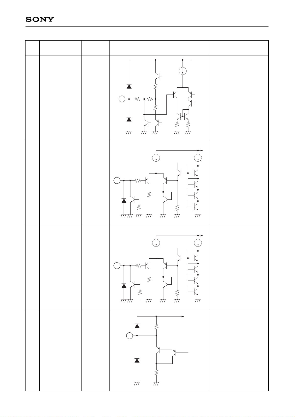
Pin Description (Ta = 25°C, VCC = 12V)
Pin
No.
Symbol Pin voltage Equivalent circuit Description
130R IN
L IN
6V Input pins.
328CL R
CL L
6V
External pins for LPF
capacitance (BASS).
427CH R
CH L
6V
External pins for HPF
capacitance (TREBLE).
5
6
7
8
BAL
TRE
BASS
VOL
4.5V
DAC output pins.
Connect LPF
capacitance of DAC.
Internal impedance is
approximetely 20kΩ.
2 GND 0V GND
30
1
130 10k
30k
10µ
V
CC
VCC/2
3
28
130
11k
250µ
V
CC
5.4k
11k
250µ
VCC/2
4
27
130
5.7k
250µ
V
CC
6k
5.7k
250µ
75µ
2k
2k
40k
20k
7.5V
5
6
7
8
VCC
Page 4

– 4 –
CXA2022S
922CC R
CC L
6V
DC-cut pins for L and R.
Internal impedance is
approximately 20kΩ.
1021ROUT
LOUT
6V Output pins.
11
17
18
19
20
23
PS1A
PS2A
PS2B
PS1B
PS3A
PS3B
6V
External capacitance
pins for surround phaseshifter. Internal
impedance is
approximately 18kΩ.
12 DET2
AGC detector output and
control pin.
9
22
500
20k
V
CC
1k
1k
500
1k
20k
10
21
500
130
V
CC
500
84k
5P
11
130
10µ
V
CC
18k
18k
17
18
19
20
23
200
V
CC
200
100k
100k
130
10k
12
Pin
No.
Symbol Pin voltage Equivalent circuit Description
Page 5
– 5 –
CXA2022S
13 HPF 6V
HPF external capacitance
pin of AGC.
14 SCL I2C bus clock line pin.
15 SDA I2C bus data line pin.
16 DET1 7.8V
AGC detector output pin.
Connect capacitance for
setting time constant.
500
130
500
10µ
10k
13
16k
16k
3k
50µ
11k
4k
100µ
VCC
56k
14
3k
50µ
4.5k
4k
100µ
VCC
56k
15
40k
V
CC
2k
16
Pin
No.
Symbol Pin voltage Equivalent circuit Description
Page 6

– 6 –
CXA2022S
24 MVFI 6V
External pin for surround
filter.
25 MVFO 6V
External pin for surround
filter.
26 VRS 6V
VCC/2 reference voltage
pin.
29 VCC 12V Power supply.
24
VCC
130
22k
22k
39k
10k
10k
18k
5µ 5µ
25
500
130
V
CC
500
30k
V
CC
30µ
30k
16k
16k
1k
26
Pin
No.
Symbol Pin voltage Equivalent circuit Description
Page 7

– 7 –
CXA2022S
Electrical Characteristics Measurement Circuit
V
CC
CH L
VRS
MVFO
MVFI
PS3B
CC L
LOUT
PS3A
PS1B
PS2B
PS2A
DET1
R IN
GND
CL R
CH R
BAL
TRE
BASS
VOL
CC R
ROUT
PS1A
DET2
HPF
SCL
SDA
L IN
CL L
CXA2022S
R IN
C1
4.7µ
R1
10k
C9
4.7µ
C3
0.1µ
C5
4700P
C7
4.7µ
C11
4.7µ
C14
4.7µ
C15
4.7µ
C24
10µ
C26
0.1µ
C17
10µ
R4
10k
ROUTCC R
C19
4700P
C21
10µ
S1
R6
1MEG
PS1A
SCL
SDA
L IN
R2
10k
C4
0.1µ
C6
4700P
C8
47µ
R3
820k
C20
8200P
C22
10µ
S5
C27
0.1µ
C28
10µ
S3
C29
4.7µ
C12
10µ
S7
C10
0.1µ
MVFI
C16
4.7µ
CC L
C13
8200P
S6
R5
10k
LOUTPS3B
C23
4700P
PS1B
C25
0.022µ
PS2B
C2
4.7µ
C18
10µ
S4 S2
PS3A PS2A
26
27
28
29
30
16
17
18
19
20
21
22
23
24
25
2
3
4
5
6
7
8
9
10
11
12
13
14 15
1
VCC
Page 8
– 8 –
CXA2022S
MODE : 00 = Surround OFF
: 01 = Simulate Stereo
: 10 = Stereo Surround 1
: 11 = Stereo Surround 2
∗ Undefined
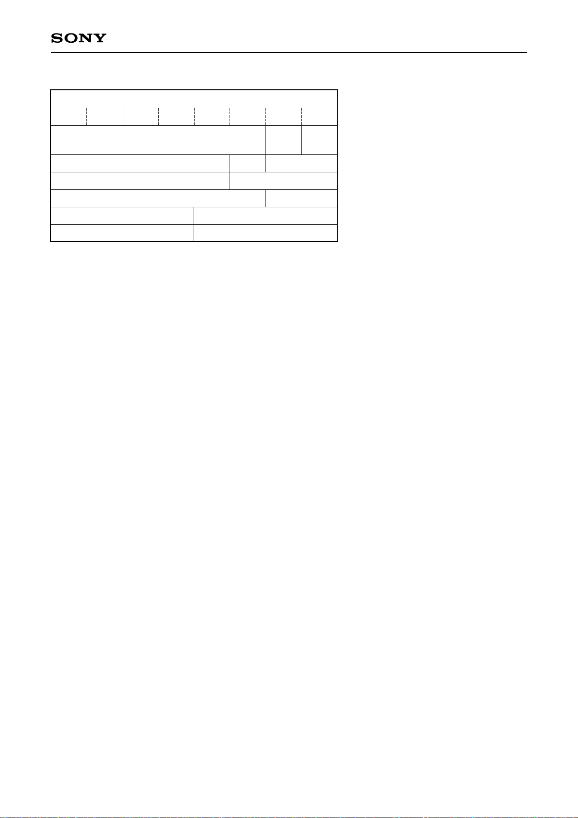
Description of Register
• VOLUME: Common to both L and R channels
0 = Minimum
3F = Maximum
• MUTE: MUTE switch
0 = Mute OFF
1 = Mute ON (muting state)
• AGC: AGC switch
0 = AGC OFF
1 = AGC ON
• BASS: Low frequency control
0 = Minimum
10 = Typical
1F = Maximum
• MODE: Surround mode setting
00 = Surround OFF
01 = Simulate Stereo (Monaural Surround)
10 = Stereo Surround 1
11 = Stereo Surround 2
• TREBLE: High frequency control
00 = Minimum
10 = Typical
1F = Maximum
Control Register Table (SLAVE ADDRESS = 82H)
DATA
bit 7 bit 6 bit 5 bit 4 bit 3 bit 2 bit 1 bit 0
MUTE
(0)
AGC
(0)
VOLUME (00)
BASS (00)
∗
MODE (00)
TREBLE (00)
∗
BALANCE (00)
∗
SURR-EFFECT (00)
MONO-EFFECT (00)
VOCAL-MIX (00)
∗
(Power ON setting value)
AGC : 0 = OFF/1 = ON
MUTE : 0 = OFF/1 = ON
Page 9
– 9 –
CXA2022S
• BALANCE: Balance control for L and R channels
00 = L channel (Minimum), R channel (Maximum)
20 = Typical
3F = L channel (Maximum), R channel (Minimum)
• SURR-EFFECT: Effect setting for Stereo Surround 1 and 2
0 = Minimum
8 = Typical
F = Maximum
• MONO-EFFECT: Effect setting for Simulate Stereo (Monaural Surround)
0 = Minimum
F = Maximum
• VOCAL-MIX: Addition amount setting of middle frequency for Stereo Surround 1 and 2
0 = Minimum
8 = Typical
F = Maximum
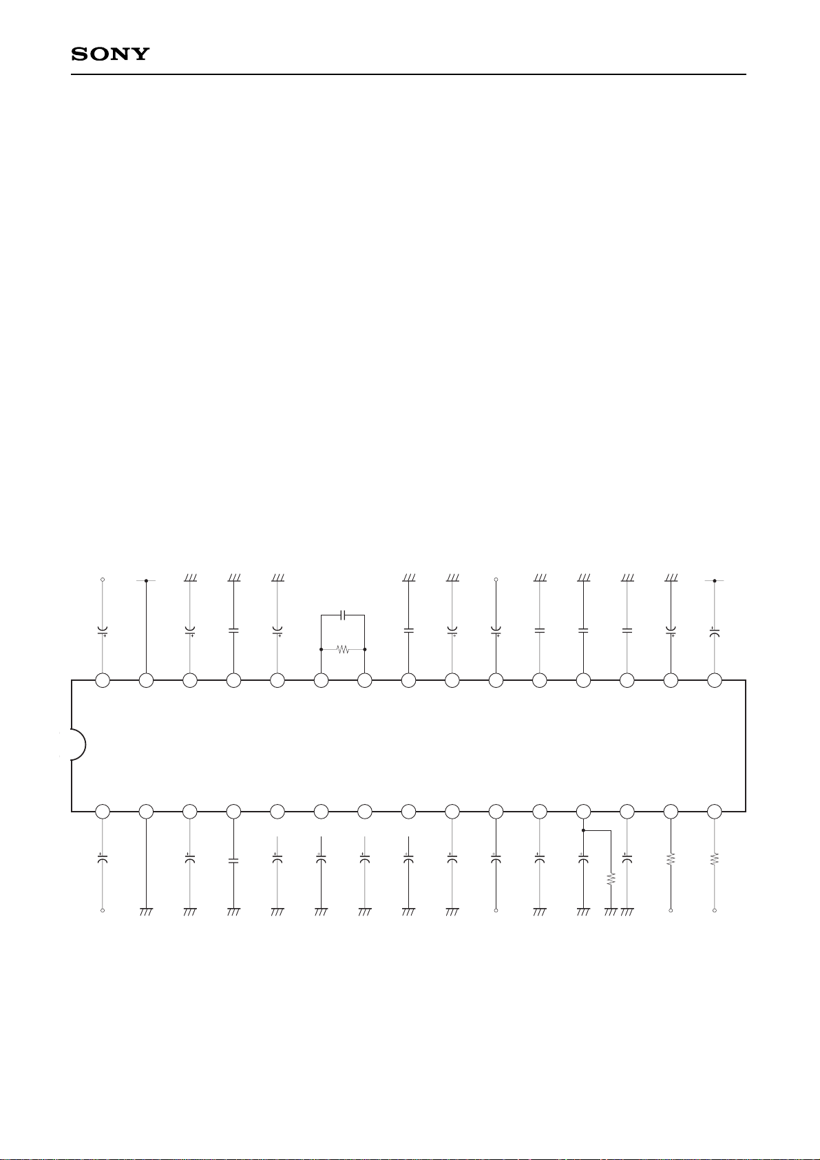
Application Circuit
V
CC
CH L
VRS
MVFO
MVFI
PS3B
CC L
LOUT
PS3A
PS1B
PS2B
PS2A
DET1
R IN
GND
CL R
CH R
BAL
TRE
BASS
VOL
CC R
ROUT
PS1A
DET2
HPF
SCL
SDA
L IN
CL L
CXA2022S
C1
4.7µ
C9
4.7µ
C3
0.1µC54700PC74.7µ
C11
4.7µ
C12
4.7µ
C14
4.7µ
C20
10µ
C22
0.1µ
C16
10µ
R2
1MEG
SCL
SDA
C4
0.1µC64700PC847µ
R1
820k
C25
4.7µ
C10
0.1µ
V
CC
R IN
R4
220
R3
220
R OUT
C18
4700P
C13
8200P
C15
4.7µ
C17
10µ
C19
8200P
C21
4700P
C23
0.022µ
C24
0.1µ
L OUT
C2
4.7µ
L IN
2
3
4
5
6
7
8
9
10
11
12
13
14 15
1
26
2728
29
30
16
17
18
19
20
21
22
23
24
25
Application circuits shown are typical examples illustrating the operation of the devices. Sony cannot assume responsibility for
any problems arising out of the use of these circuits or for any infringement of third party patent and other right due to same.
Page 10

– 10 –
CXA2022S
No.
1
2
3
4
5
6
7
8
9
10
11
12
13
14
15
Current
consumption
FLAT
L, R
REF, Level
L, R
VOL MIN
L, R
FLAT
f characteristics
100Hz
FLAT
f characteristics
10kHz
BASS BOOST
100Hz
TREBLE BOOST
10kHz
BASS CUT
100Hz
TREBLE CUT
10kHz
BALANCE
BOOST L
BALANCE
CUT L
BALANCE
BOOST R
BALANCE
CUT R
Distortion
L, R
I
CC
VF L, R
VR L, R
VMIN L, R
VLF L, R
VHF L, R
VBST LF
VBST HF
VCUT LF
VCUT HF
VBAL BST L
VBAL CUT L
VBAL BST R
VBAL CUT R
Vdist
3F
20
0
20
3F
0 0 10
1F
0
10
0 10
1F
0
10
20
3F
0
3F
20
8 8 8
L-IN
R-IN
1kHz
2.4Vrms
100Hz
2.4Vrms
10kHz
2.4Vrms
100Hz
2.4Vrms
10kHz
2.4Vrms
100Hz
2.4Vrms
10kHz
2.4Vrms
1kHz
2.4Vrms
LOUT
ROUT
LOUT
ROUT
LOUT
ROUT
REF: INPUT
REF: V
R L, R
20
–2.0
–17
—
–1.5
–1.5
8.5
8.5
–13.5
–13.5
0
—
0
—
—
35
0
–14
—
0
0
11
11
–11
–11
1.2
—
1.2
—
—
55
2.0
–11
–70
1.5
1.5
13.5
13.5
–8.5
–8.5
2.0
–30
2.0
–30
2.0
mA
dB
dB
dB
dB
dB
dB
dB
dB
dB
dB
dB
dB
dB
%
VOL MUTE AGC BASS MODE TRE BAL S-EFF M-EFF V-MIX
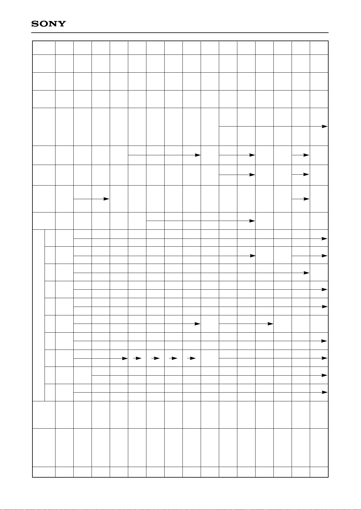
Electrical Characteristics (Ta = 25°C, VCC = 12V)
Measurement
item
Signal
Input conditions
Input
point
Input signal
SW set
to ON
Measure-
ment
point
Remarks Min. Typ. Max. Unit
Page 11
– 11 –
CXA2022S
No.
16
17
18
19
20
21
22
23
24
25
26
27
28
29
30
Mute L, R
Crass-Talk
L → R
Crass-Talk
R → L
NOISE
LEVEL L, R
AGC
BOOST L, R
AGC
BOOST L, R
AGC
NULL L, R
AGC
CUT L, R
MONO
FIL 100HZ
MONO
FIL 500HZ
MONO
FIL 10kHz
MS MIX
LEVEL L, R
SS DIF
GAIN L
SS DIF
GAIN R
SS MIX
LEVEL L
V
MT L, R
VCT L, R
VCT R, L
VNOI L, R
VGCB L, R
VGCB2 L, R
VGCN L, R
VGCC L, R
MFL L
MFL M
MFL H
MMX L, R
SDG L
SDG R
SMX L
3F 1
0
0
0
10 0
1
2
3
2
10 20 8
F
8
F
8
8
L-IN
R-IN
L-IN
R-IN
L-IN
R-IN
PS1A
L-IN
R-IN
PS1A
1kHz
2.4Vrms
1kHz
10mVrms
1kHz
50mVrms
1kHz
160mVrms
1kHz
2Vrms
100Hz
1.25Vrms
500Hz
1.25Vrms
10kHz
1.25Vrms
1kHz
350mVrms
1kHz
2.5Vrms
1kHz
350mVrms
SW2
SW1
SW4
SW1
LOUT
ROUT
ROUT
LOUT
LOUT
ROUT
PS2B
LOUT
ROUT
PS1B
LOUT
REF: INPUT
REF: V
FR
REF: VFL
REF: AGC-OFF
(0)
REF: AGC-OFF
(0)
REF: AGC-OFF
(0)
REF: AGC-OFF
(0)
REF: INPUT
—
—
—
—
0.5
5
–2.5
–24
–11
–18
–1.5
13
–4
–4
13
—
—
—
—
3
7
–0.5
–20
–8.5
–15.5
1.0
16
–2
–2
16
–70
–70
–70
–60
5.5
10
2
–16
–6
–13
3.5
19
0
0
19
dB
dB
dB
dBm
dB
dB
dB
dB
dB
dB
dB
dB
dB
dB
dB
VOL MUTE AGC BASS MODE TRE BAL S-EFF M-EFF V-MIX
0
1
0
1
0
1
0
1
Measurement
item
Signal
Input conditions
Input
point
Input signal
SW set
to ON
Measure-
ment
point
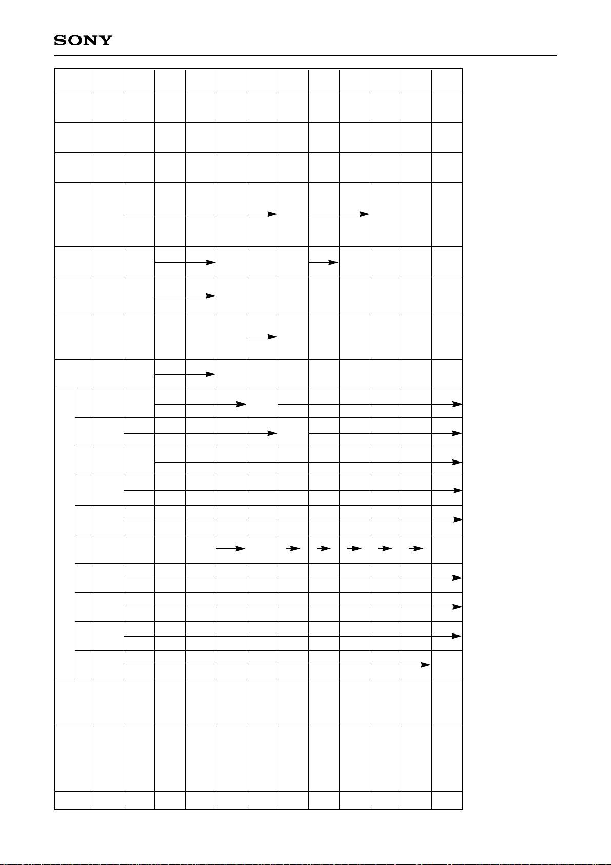
Remarks Min. Typ. Max. Unit
Page 12
– 12 –
CXA2022S
No.
31
32
33
34
35
36
37
38
39
40
41
42
SS MIX
LEVEL R
V-FIL
100HZ
V-FIL
1kHz
V-FIL
10kHz
V-MIX
L, R
SS2-MIX
DC OFF-Set
OFF → MS-L, R
DC OFF-Set
OFF → SS1-L, R
DC OFF-Set
OFF → SS2-L
DC OFF-Set
SS2 → MS-L, R
DC OFF-Set
SS1 → MS-L
VOL MIN
NOISE L, R
S
MX R
VFIL L
VFIL M
VFIL H
VMX L, R
SS2MX
DOOM
DOOSS1L, R
DOOSS2
DOSS2M L, R
DOSS1M
VMINNO L, R
3F
0
0 0 10 3
2
3
2
3
0
10 20 F
8
8
F
8
F
8
PS1A
L-IN
R-IN
MVFI
PS3A
1kHz
350mVrms
100Hz
2.5Vrms
1kHz
2.5Vrms
10kHz
2.5Vrms
1kHz
500mVrms
SW1
SW6
SW7
SW5
ROUT
PS3B
LOUT
ROUT
LOUT
LOUT
ROUT
LOUT
LOUT
ROUT
LOUT
LOUT
ROUT
REF: INPUT
REF: MODE0
REF: MODE3
REF: MODE2
30kHz LPF
13
–7.5
–3
–10.5
10.5
11
–150
–150
–150
–150
–150
—
16
–5
–0.5
–8
13.5
14
0
0
0
0
0
–92
19
–2.5
2
–5.5
16.5
17
150
150
150
150
150
–85
dB
dB
dB
dB
dB
dB
mV
mV
mV
mV
mV
dBm
Measurement
item
Signal
Input conditions
VOL MUTE AGC BASS MODE TRE BAL S-EFF M-EFF V-MIX
Input
point
Input signal
SW set
to ON
Measure-
ment
point
Remarks Min. Typ. Max. Unit
0
1
0
2
0
3
3
1
2
1
Page 13

– 13 –
CXA2022S
Description of Operation
• AGC circuit
The AGC circuit is provided at the input. When AGC is set to ON, this circuit is 0dB for small signal input,
boosts for medium signal input, and achieves gain reduction for large signal input. The sound level
defference between input sources can be absorbed at this circuit.
• Surround circuit
The surround circuit provides three modes; MONO (Simulate Stereo), STEREO-1 and STEREO-2.
MONO mode
L + R signals, passed through the mono filter and then through four stages of phase shifters (PS1A, PS1B,
PS2A, PS2B) and 9kHz LPF, are added to L and R channels at opposite phase to each other.
The surround effect can be changed by the MONO-EFFECT.
STEREO-1 mode
L-R signals, passed through two stages of phase shifters (PS1A, PS1B) and 9kHz LPF, are added to L and R
channels at opposite phase to each other. The surround effect can be changed by the SURR-EFFECT. In
addition, L + R signals passed through the middle frequency BPF (1kHz BPF) are added to L and R channels at
in-phase to each other to prevent "vocal missing" in the surround mode. The addition amount of middle
frequency can be changed by the VOCAL-MIX.
STEREO-2 mode
L-R signals, passed through two stages of phase shifters (PS1A, PS1B) and 9kHz LPF, are added to L and R
channels at opposite phase to each other. The surround effect can be changed by the SURR-EFFECT. In
addition, L + R signals passed through the middle frequency BPF (1kHz BPF) are added to R channel, and the
middle frequency signals passed further through two stages of phase shifters (PS3A, PS3B) are added to the L
channel. The addition amount of middle frequency (L and R) can be changed by the VOCAL-MIX.
Phase Shifter
Each of the phase shifters PS1, PS2 and PS3 consists of two stages of phase shifters (A, B). The transfer
function for a stage of phase shifter is expressed by the following equation.
VO = Vin
R: Internal resistance ≈ 18kΩ, C: External capacitance
• TONE circuit
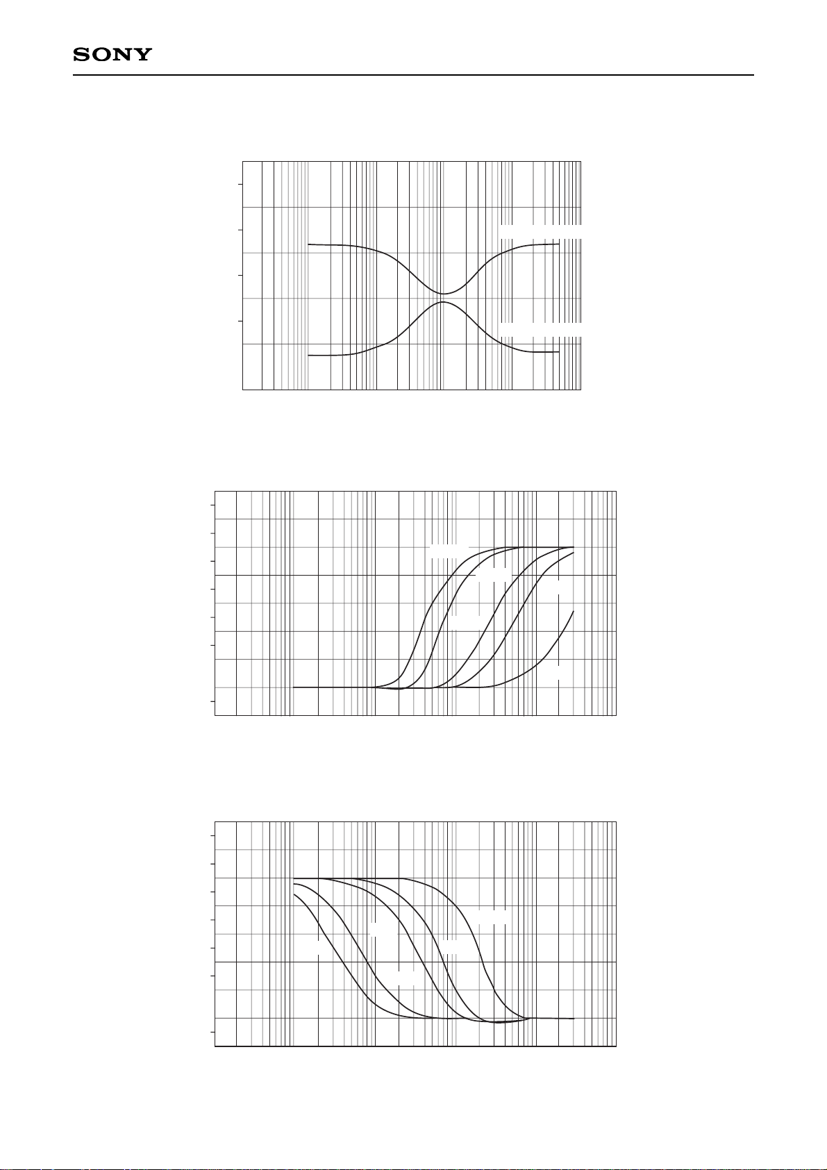
Provides tone controls for BASS and TREBLE. The external capacitance of CL for BASS and CH for TREBLE
can determine the characteristics. The number of steps is 32.
• BALANCE and VOLUME circuit
Provides controls for BALANCE and VOLUME. the number of steps is 64 each.
• DAC circuit
Provides controls for BASS, TREBLE, VOLUME and BALANCE. The internal impedance is approximately
20kΩ and the LPF capacitance is used externally.
1 – SCR
1 + SCR
Page 14
– 14 –
CXA2022S
CH. vs. TREBLE-CONTROL (MAX)
–2.5
0.0
10.0
17.5
OUT L, R [dB]
2.5
15.0
12.5
7.5
5.0
10 1k 10k
Frequency [Hz]
100 100k
470p
2200p
0.022µ
4700p
0.047µ
CH. vs. BASS-CONTROL (MAX)
–2.5
0.0
10.0
17.5
OUT L, R [dB]
2.5
15.0
12.5
7.5
5.0
10 1k 10k
Frequency [Hz]
100 100k
0.1µ
0.047µ
0.47µ
0.01µ
1µ
–20
–10
0
10
20
OUT L, R [dB]
100 1k 10k
Frequency [Hz]
TONE characteristics
BASS-TREBLE MAX.
BASS-TREBLE MIN.
10 100k
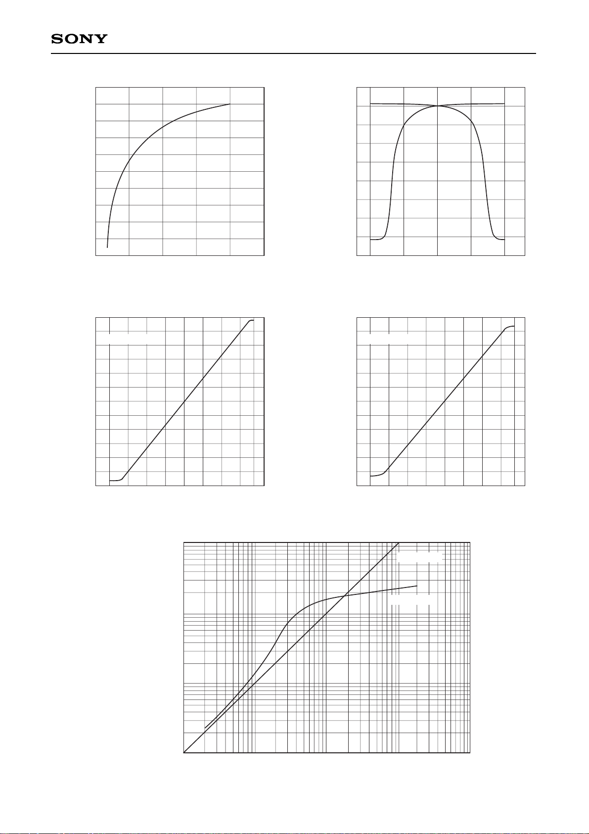
Example of Representative Characteristics
Page 15
– 15 –
CXA2022S
–80
–70
–50
–30
–10
OUT L, R [dB]
10 20 30
BUS Data (VOL)
VOL CONTROL characteristics
3F
–60
–40
–20
0
–12
–10
0
4
OUT L, R [dB]
4 8 C
BUS Data (BASS)
BASS CONTROL characteristics
10
–2
2
6
0 18 1C 1F14
Input = 100Hz
–6
–8
–4
8
10
12
–80
–70
–50
–30
–10
OUT L, R [dB]
10 20 30
BUS Data (BALANCE)
BALANCE CONTROL characteristics
3F
–60
–40
–20
0
0
OUT R OUT L
AGC characteristics
10
1V
OUT [rms]
100mV
10 1V
IN [rms]
100mV
AGC = ON
AGC = OFF
–12
–10
0
4
OUT L, R [dB]
4 8 C
BUS Data (TREBLE)
TREBLE CONTROL characteristics
10
–2
2
6
0 18 1C 1F14
Input = 10kHz
–6
–8
–4
8
10
12
Page 16
– 16 –
CXA2022S
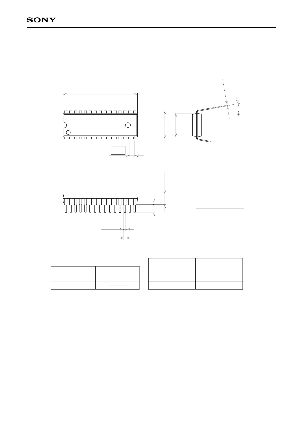
Package Outline Unit : mm
SONY CODE
EIAJ CODE
JEDEC CODE
30PIN SDIP (PLASTIC)
26.9 – 0.1
+ 0.4
15
16
30
1.778
10.16
8.5 – 0.1
+ 0.3
0.25 – 0.05
+ 0.1
0° to 15°
0.5 ± 0.1
0.9 ± 0.15
3.0 MIN
0.5 MIN
3.7 – 0.1
+ 0.4
SDIP-30P-01
SDIP030-P-0400
1
PACKAGE STRUCTURE
MOLDING COMPOUND
LEAD TREATMENT
LEAD MATERIAL
PACKAGE MASS
EPOXY RESIN
PLATING
COPPER ALLOY
1.8g
SOLDER/PALLADIUM
1.All mat surface type.
Two kinds of package surface:
2.All mirror surface type.
NOTE : PALLADIUM PLATING
This product uses S-PdPPF (Sony Spec.-Palladium Pre-Plated Lead Frame).
 Loading...