

Page 1
—1—
E95422B78-TE
Sony reserves the right to change products and specifications without prior notice. This information does not convey any license by
any implication or otherwise under any patents or other right. Application circuits shown, if any, are typical examples illustrating the
operation of the devices. Sony cannot assume responsibility for any problems arising out of the use of these circuits.
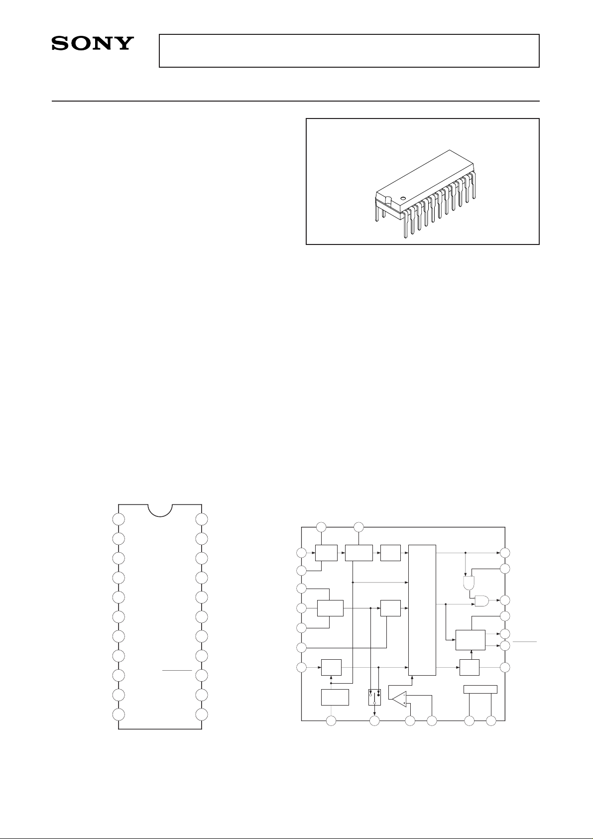
Sync Identification for CRT Display
22 pin SDIP (Plastic)
CXA2016S
Absolute Maximum Ratings (Ta=25°C)
• Supply voltage VCC 12 V
• Operating temperature Topr –20 to +75 °C
• Storage temperature Tstg –65 to +150 °C
• Allowable power dissipation
PD 962 mW
Operating Conditions
Supply voltage VCC 5 ± 0.25 V
Description
The CXA2016S is used for sync signal
identification and waveform shaping in the CRT
computers display for multi-scan system. There are
three types of sync input signals for identification:
separate sync, composite sync, and sync on video
signals.
Features
• Power save function available (5 V power supply)
• Clamp pulse output position selectable among sync
interval, back porch interval, and AUTO.
• Polarity information of sync signals is output.
• Polarity and amplitude of input signals:
Polarity
Amplitude (Vp-p)
V. separate sync: Positive/Negative 1 to 5
H. separate sync: Positive/Negative 1 to 5
Composite sync: Positive/Negative 1 to 5
Sync on video:
Sync signals part of Negative 0.2 to 0.4
Video part 0 to 1.4
Applications
CRT display monitor
Pin Configuration (Top View) Block Diagram
1
2
3
4
5
6
7
8
9
10
11 12
13
14
15
16
17
18
19
20
21
22
VS IN
PVC
EVC
CS IN
PHC
EHC
Video IN
HD SEL
ISC
ISJ
GND
V
CC
VD
V
SS IN
V
SS OUT
HD
PV
PH
CLP SEL
CLP OUT
V
SS REF
CLP OUT
Polarity
Check
V. Ramp
Generator
Exist
Check
Polarity
Check
Exist
Check
Sync
Sep
Level
Control
Bias
Sync
Check
Logic
Clamp
Pulse
Generator
21
8
18
9
13
14
15
10 19 20 12 2211
1
17
16
4
5
6
7
2 3
PVC EVC
VS IN
PV
PH
CS IN
PHC
EHC
Video IN
ISJ VSS OUT VSS IN VSS REF GND VCC
VD
HD SEL
HD
ISC
CLP OUT
CLP SEL
CLP OUT
Page 2
—2—
CXA2016S
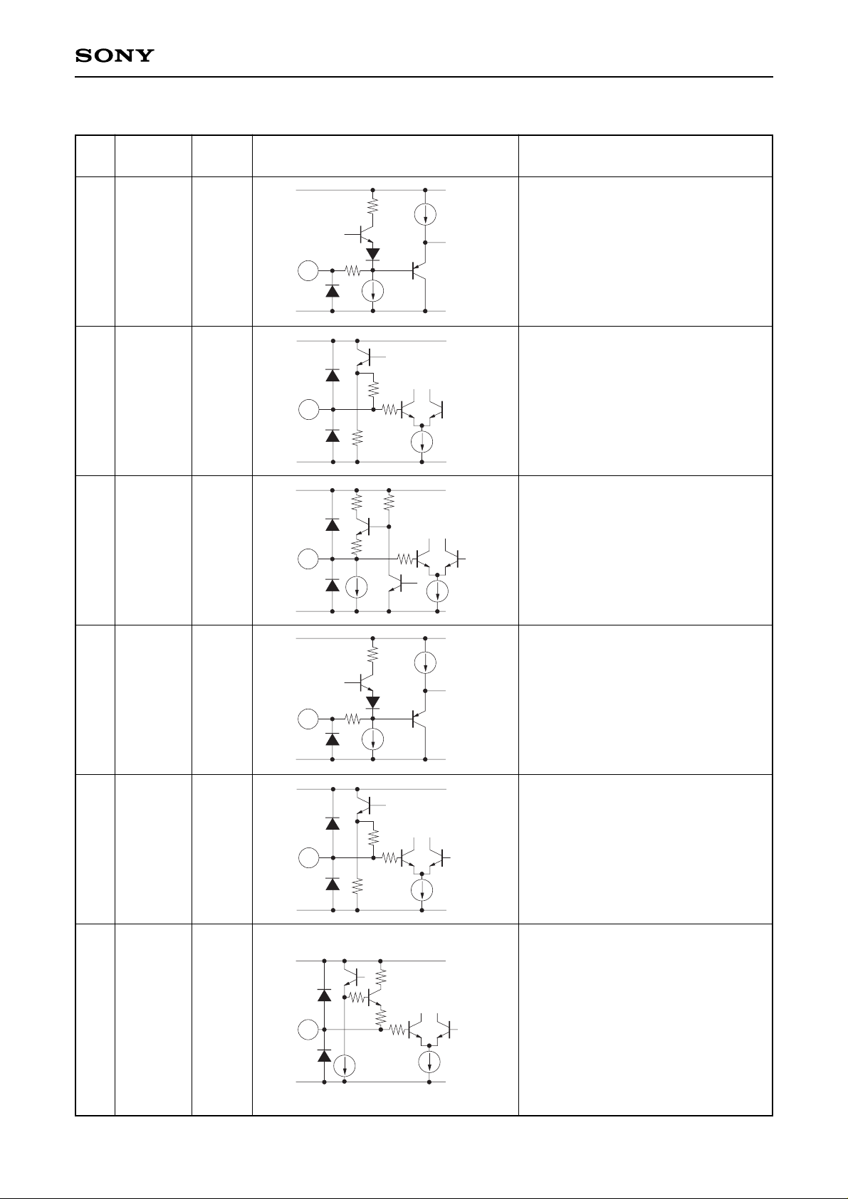
Pin Description (Ta=25 °C, VCC=5 V)
Pin
Symbol
Pin
Equivalent circuit Description
No voltage
VCC
GND
1
100
1k
VCC
GND
2
1k
96k
8k
1k
3
200
200
200
1k
VCC
GND
VCC
GND
100
1k
4
VCC
GND
96k
8k
1k
5
6
1k
100
1k
1k
VCC
GND
VS IN
PVC
EVC
CS IN
PHC
EHC
2.6 V
—
—
2.6 V
—
—
V. separate sync (positive/negative
polarity) as capacitor input. Amplitude
is 1 to 5 Vp-p.
This pin connects a 0.22 µF
integrating capacitor for the vertical
signal polarity check circuit to GND.
When connecting the capacity at
positive polarity, it is 2.9 V and at
negative polarity, 120 mV.
V. ramp waveforms generation part of
vertical signal exist check circuit.
Generates ramp waveforms
synchronously with the input signal
cycle and connects 0.22 µF to GND.
Inputs composite sync
(positive/negative polarity) and H.
separate sync (positive/negative
polarity) as capacitor input. Amplitude
is 1 to 5 Vp-p.
This pin connects a 0.1 µF integrating
capacitor for the horizontal signal
polarity check circuit to GND. When
connecting the capacity at positive
polarity, it is 2.6 V and at negative
polarity, 350 mV.
A 33 kΩ resistance and a nearly peak
hold circuit for 0.22 µF capacitor are
connected to this pin for input signal
exist check at CS IN input pin. When
a signal is input at CS IN pin, a nearly
peak hold is executed at 2.1 V to 2.7
V, a comparison is made with the 1.4
V reference voltage, and input signal
exist is identified.
1
2
3
4
5
6
Page 3
—3—
CXA2016S
7
2k
VCC
GND
8
1k
VCC
GND
9
2k 1k
VCC
GND
50k
100
4k 1k
VCC
GND
50k
100
10
12
12k
20k
1k
VCC
GND
7
8
9
10
11
12
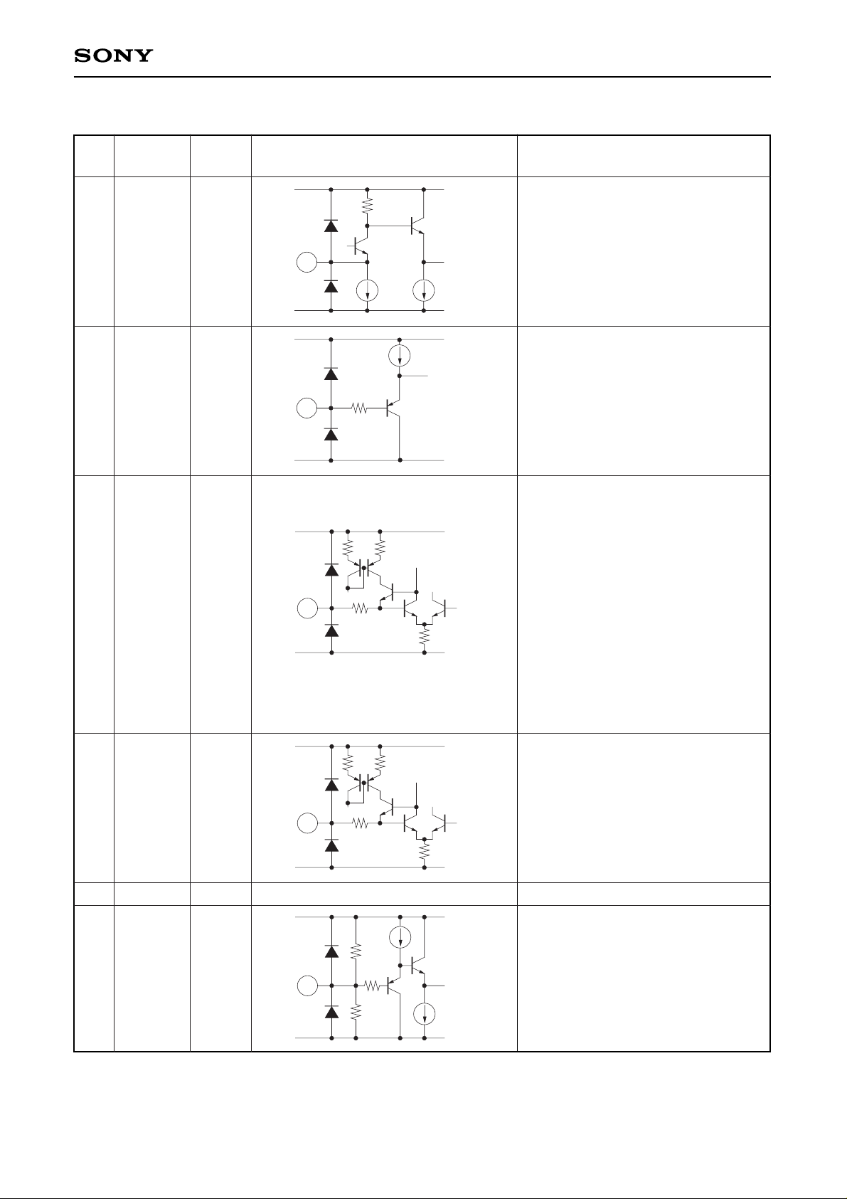
Video IN
HD SEL
ISC
ISJ
GND
VSS REF
—
—
1.2 V
1.2 V
0 V
3.125 V
Inputs sync on video (sync at negative
polarity). Connects in series a 1 µF
capacitor and a 270 Ω resistance to
input signals.
Selects output processing of HD
(H. Drive Pulse) at a VD interval.
Input at TTL level.
When Low level is selected, HD is not
output at a VD interval.
When High level is selected, HD is
output at the VD interval.
Resistance connecting pin for
reference current source of clamp
pulse output circuit, and connects 12
kΩ resistance to GND. When a 12 kΩ
resistance is connected, a 100 µA
current flows through this pin (pulse
width is approximately 300 ns).
Clamp pulse output pulse width is
varied by changing the value of the
resistance.
∗
Use a metal film resistor with an
accuracy of ±1 %
Resistance connecting pin for
reference current source and
connecting 12 kΩ resistance to GND.
When the resistance is connected, a
100 µA current flows through this pin.
∗
Use a metal film resistor with an
accuracy of ±1 %
GND pin.
Reference pin for V. sync separator of
composite sync and video sync.
—
Pin
Symbol
Pin
Equivalent circuit Description
No voltage
Page 4
—4—
CXA2016S
13
14
15
16
17
18
19
20
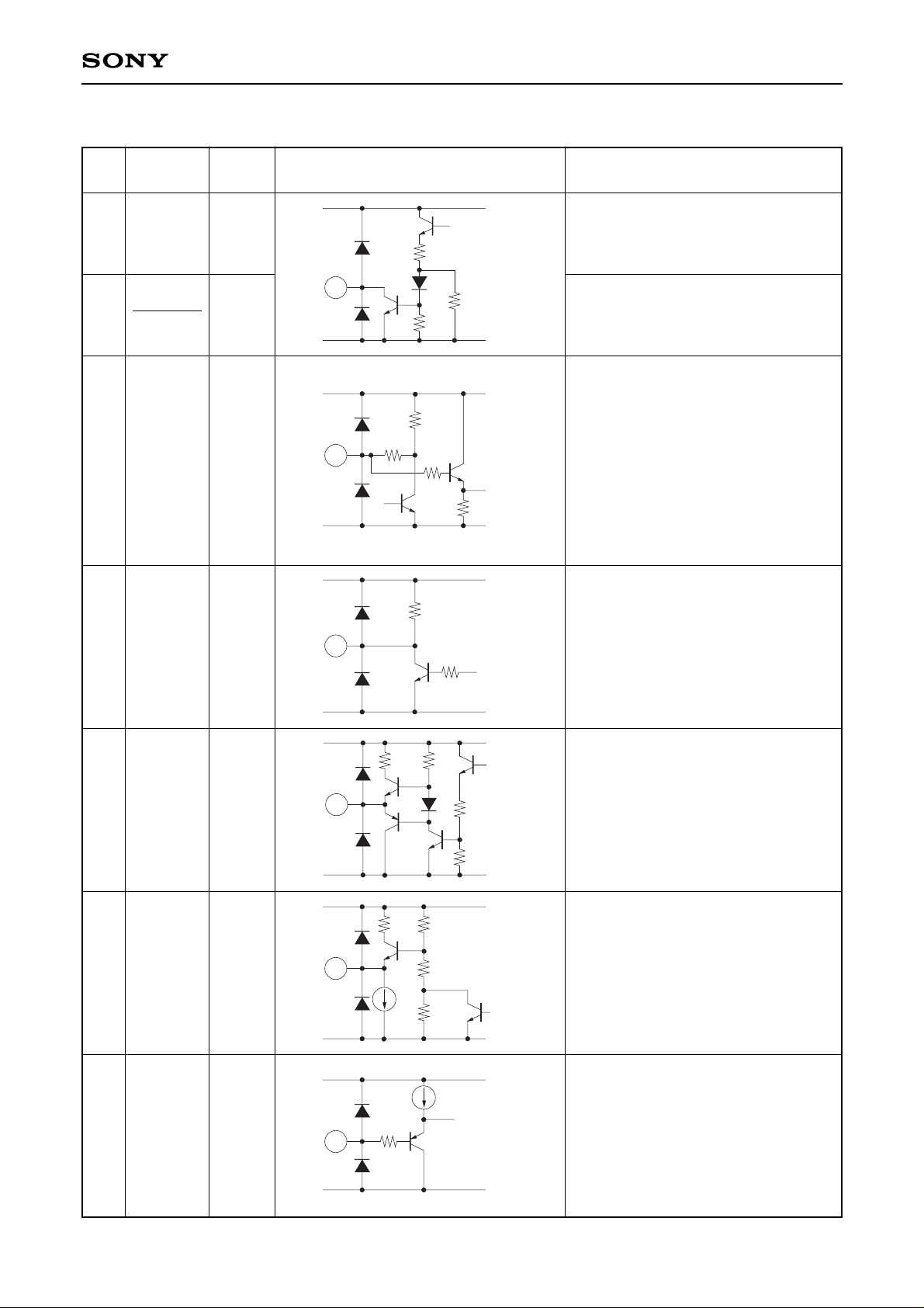
CLP OUT
CLP OUT
CLP SEL
PH
PV
HD
VSS OUT
VSS IN
—
—
—
—
—
—
—
Clamp pulse output; Open collectortype pin at positive polarity.
Clamp pulse output; Open collectortype pin at negative polarity.
Selects output position of a clamp
pulse. Input at TTL level.
When Low level is selected, a clamp
pulse is output at a back porch
interval.
When High level is selected, clamp
pulse is output at a sync interval.
See the Description of Operation for
Input/Output Matrix.
Output polarity information of
horizontal and vertical sync signals.
See the Description of Operation for
Input/Output Matrix.
HD (H. Drive Pulse) output; Push-pull
type pin at positive polarity.
Composite sync or sync signal
separated from video sync is output.
Output is at positive polarity.
Input for V. sync separator
comparator. Integrates the output at
Pin 19 and inputs it.
Pin
Symbol
Pin
Equivalent circuit Description
No voltage
VCC
13
15
500
40k
7k
GND
VCC
30k
20k
1k
43k
GND
VCC
20k
16
20k
GND
18
19
20
333 6k
200 5k
1k
2.5k
17.5k
6k
6k
VCC
GND
VCC
GND
VCC
GND
Page 5

—5—
CXA2016S
21
22
VD
VCC
—
5 V
VD (V. Drive Pulse) output pin.
Output is at positive polarity.
Power supply pin.
Pin
Symbol
Pin
Equivalent circuit Description
No voltage
—
VCC
10k
21
10k
10k
GND
Page 6

—6—
CXA2016S
No. Item
Symbol
Measurement contents
Measurement
Min. Typ. Max. Unit
point
VD output
voltage
HD output
voltage
Clamp pulse
output voltage
Clamp pulse
output pulse
width
HD delay
Clamp pulse
delay
Polarity
identification
output voltage
Current
consumption
Measure VD output peak value
during V. separate sync input.
Input signal A. (tw=60 µs)
Measure HD output peak value
during sync on video input.
Input signal C. (tw=1 µs)
Measure clamp pulse output peak
value during composite sync input.
Input signal B. (tw=1 µs)
Measure clamp pulse output pulse
width during composite sync input.
Input signal B. (tw=1 µs)
Measure delay difference between
CS and HD during composite sync
input. Or the time from CS
(positive polarity) rise time (50 %)
to HD output rise time (50 %).
Input signal D.
Measure delay difference between
HD and clamp pulse during
composite sync input. Or the time
from HD output fall time (50 %) to
clamp pulse output rise time∗1(50
%). Input signal B.
Sync signal polarity information
is output.
Measure high level voltage.
(No load)
Sync signal polarity information
is output.
Measure low level voltage.
(No load)
VCC=5 V. Measure current
consumption during no signal input.
1
2
3
4
5
6
7
8
EVD
EHD
ECP
tC
thd
tcd1
PN
PP
ICC
VD
(Pin 21)
HD
(Pin 18)
CLAMP
(Pin 13)
CLAMP
(Pin 14)
CLAMP
(Pin 13)
CLAMP
(Pin 14)
HD
(Pin 18)
CLAMP
(Pin 13)
CLAMP
(Pin 14)
PH, PV
(Pins 16
and 17)
PH, PV
(Pins 16
and 17)
VCC
(Pin 22)
High level
4.3 4.9 —
Low level
— 0.1 0.4
High level
3.3 4.2 —
Low level
— 0.3 0.5
High level
4.3 4.9 —
Low level
— 0.3 0.8
High level
4.3 4.9 —
Low level
— 0.4 0.9
260 305 380
260 310 380
— 75 100
— 5.0 30
— 5.0 30
4.3 — —
— — 0.4
— 26.5 45
V
V
V
V
ns
ns
ns
ns
V
V
mA
Electrical Characteristics (Ta=25 °C, VCC=5 V. See the Electrical Characteristics Measurement Circuit.)
∗1 CLAMP is for the fall time.
Page 7
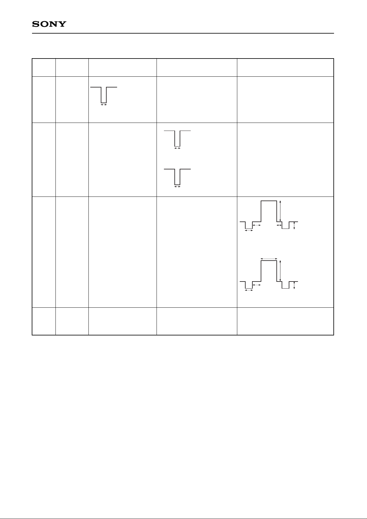
—7—
CXA2016S
Video IN (Pin 7)
fV=40 Hz
tWV=60 µs
fH=50 kHz
tWH=1 µs
Signal
A
B
C
D
Composite SYNC IN (Pin 4)
fv=40 Hz
tWV=60 µs
Negative logic
1 Vp-p
fH=50 kHz
tWH=1 µs
Negative logic
1 Vp-p
fH=50 kHz
tWH=1 µs
Positive logic 1 Vp-p
Item
1
3, 4, 6
2
5
V. SYNC IN (Pin 1)
fv=40 Hz
tWV=60 µs
Negative logic
1 Vp-p
V
1WV
H
1WH
V
60µs
10H 3H
0.7V
0.2V
H
1µs
3µs
0.7V
0.2V
15µs
Types of Signal Source
1WV
Page 8
—8—
CXA2016S
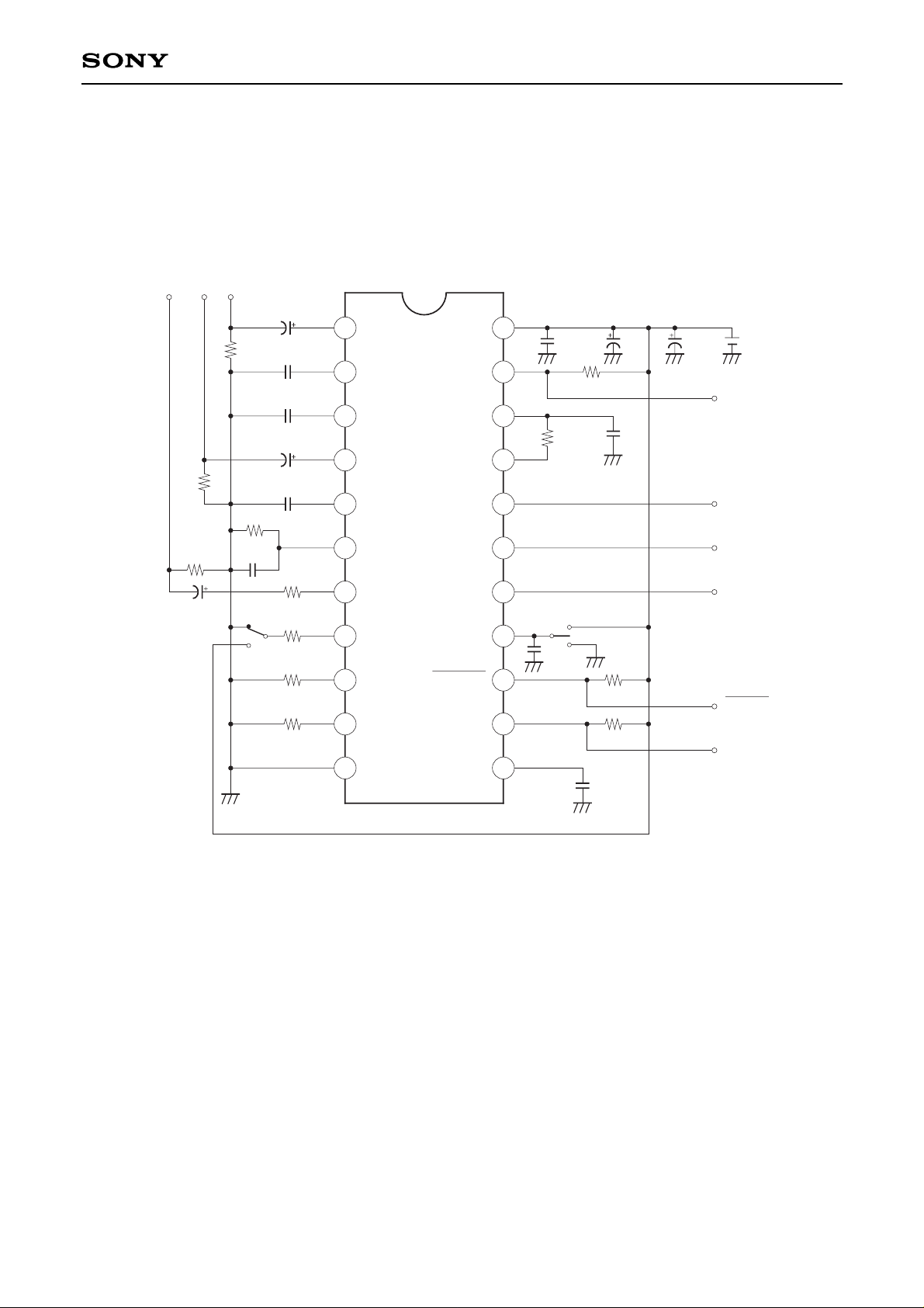
Electrical Characteristics Measurement Circuit
CLAMP
PH
PV
VD
2.2k
HD
CLAMP
220
VS IN
PVC
EVC
CS IN
PHC
EHC
Video IN
HD SEL
ISC
ISJ
GND
1
2
3
4
5
6
7
8
9
10
11
VCC
VD
V
SS IN
V
SS OUT
HD
PV
PH
CLP SEL
CLP OUT
CLP OUT
V
SS Ref
Video
Sync
HS
or
CS VS
75
75
2.2µ
0.22µ
0.22µ
1µ
0.1µ
33k
0.22µ
75
1µ
10k
12k
12k
1µ 10µ
5V
1k
3300p
0.01µ
1k
1k
0.1µ
22
21
20
19
18
17
16
15
14
13
12
0.01µ
Page 9
Description of Operation
Input signal
• VS IN (Pin 1)
fV : 40 to 200 Hz
VS : 1 to 5Vp-p (positive/negative polarity)
• HS IN (Pin 4)
fH : 15k to 130 kHz
VS : 1 to 5 Vp-p (positive/negative polarity)
• CS IN (Pin 4)
fH : 15 k to 130 kHz
fV : 40 to 200 Hz
VS : 1 to 5 Vp-p (positive/negative polarity)
• Video IN (Pin 7)
fH : 15 k to 130 kHz
fV : 40 to 200 Hz
VV : 0 to 1.4 Vp-p
VS : 0.2 to 0.4 Vp-p
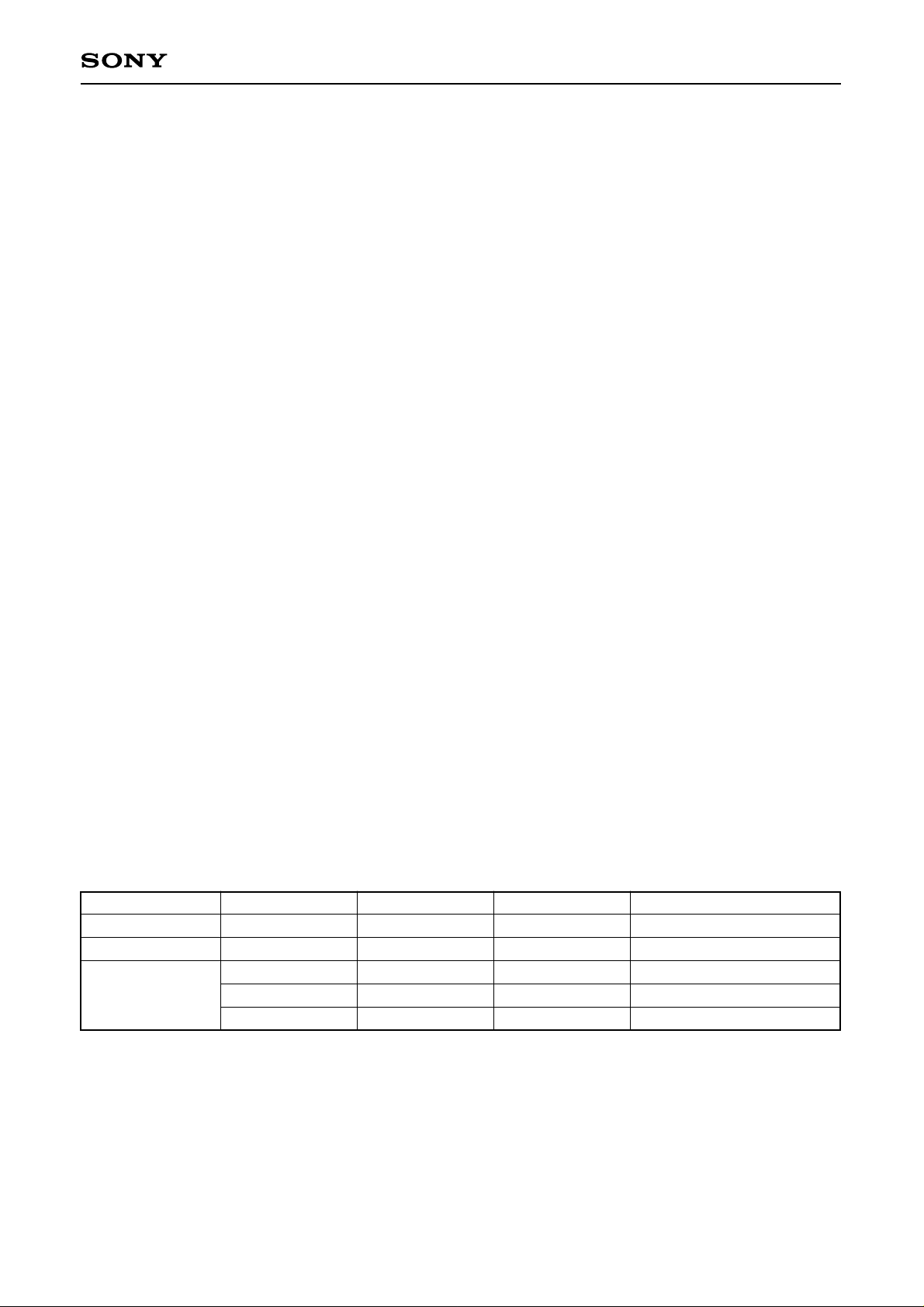
Clamp Pulse Output
• Clamp pulse (Pins 13 and 14) is output under the following conditions.
Pin 13 is for open collector output and is at positive polarity.
Pin 14 is for open collector output and is at negative polarity.
td: Clamp pulse delays for 10 to 20 ns from HD.
tw: Clamp pulse width varies depending on the value of the resistance connected to Pin 9.
<Conditions>
(1) When CS IN or Video IN is selected, a clamp pulse at the VD interval is not output.
(2) During H./V. Separate Sync, a clamp pulse at the VD interval is also output.
(3) When Pin 15 (CLP SEL) is connected to GND, a clamp pulse is output at the back porch interval. When
Pin 15 (CLP SEL) is connected to VCC, a clamp pulse is output at the SYNC interval. If a capacitor is
connected between this pin and GND, the output position is automatically selected.
Clamp Pulse Input/Output Matrix
—9—
CXA2016S
CLP SEL VS IN CS IN Video IN Clamp pulse output position
GND ∗ ∗ ∗ Back porch interval
VCC ∗ ∗ ∗ SYNC interval
∗ — O Back porch interval
AUTO ∗ O — SYNC interval
∗ — — (Back porch interval)
[O] indicates that input SYNC exists.
[—] indicates no signal (no SYNC).
[ ∗ ] has no relation with input signal.
Page 10
—10—
CXA2016S
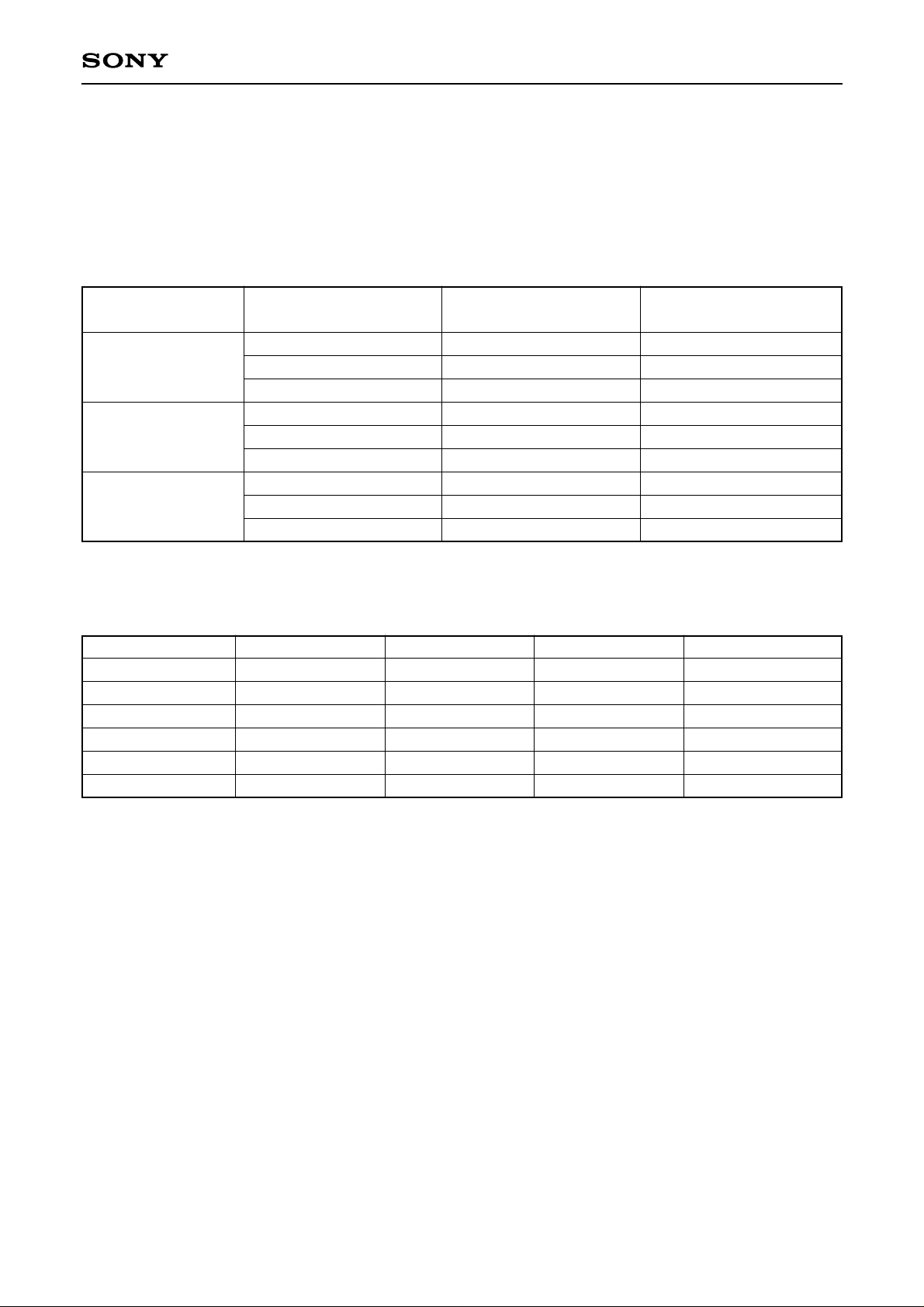
HD Select Function
When HD SEL is Low, HD at the VD interval is not output.
When HD SEL is High, HD at the VD interval is output.
During separate sync output, HD is output regardless of HD SEL.
Mode Matrix of SYNC Polarity Identification Signal
VS IN CS IN PV out PH out
(
Pin 1) (Pin 4) (Pin 17) (Pin 16)
No signal Low Low
VS (positive polarity) HS (positive polarity) Low Low
HS (negative polarity) Low High
No signal High Low
VS (negative polarity) HS (positive polarity) High Low
HS (negative polarity) High High
No signal Low Low
No signal COMP (positive polarity) Low Low
COMP (negative polarity) Low High
VS IN CS IN Video IN VD OUT HD OUT
O O
∗ VS CS
—
O
∗ CS CS
— —
O
Video Video
— — — (Video) (Video)
O
—
O
VS Video
O
— — VS (Video)
Note) The corresponding sync signals are input to VSIN and Video IN.
[O] indicates that input SYNC exists.
[—] indicates no signal.
[ ∗ ] has no relation with input signal.
Low level: 0 to 0.4 V, High level: VCC
Input/Output Matrix
Page 11
—11—
CXA2016S
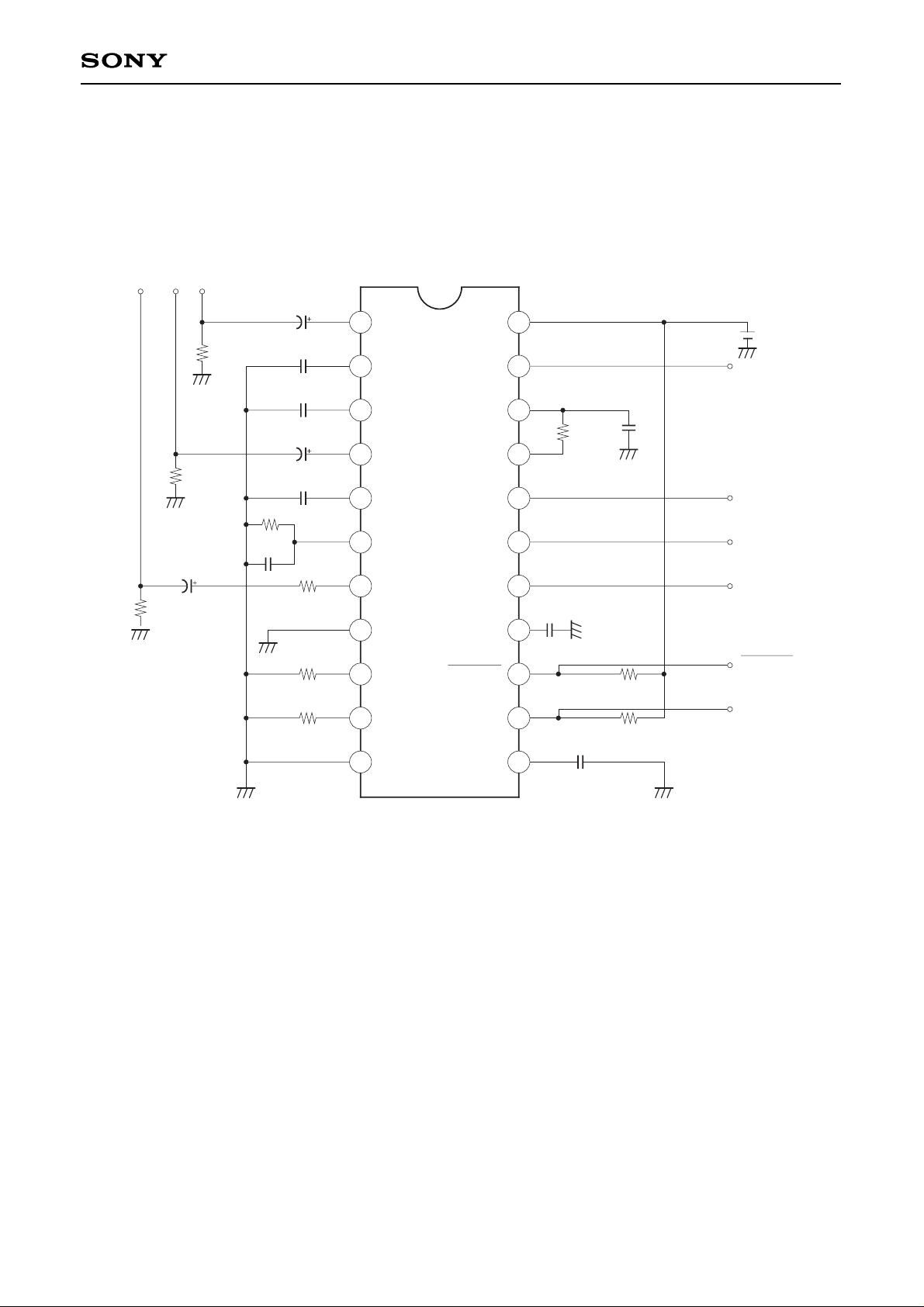
Application Circuit
CLP OUT
PH
PV
VD OUT
2.2k
HD OUT
CLP OUT
VS IN
PVC
EVC
CS IN
PHC
EHC
Video IN
HD SEL
ISC
ISJ
GND
VCC
VD
V
SS IN
V
SS OUT
HD
PV
PH
CLP SEL
CLP OUT
CLP OUT
V
SS Ref
VS
75
2.2µ
0.22µ
1µ
0.1µ
33k
0.22µ
12k∗
12k∗
3300p
1k
1k
0.1µ
0.22µ
270
75
0.01µ
VCC
5V
75
Video
(G)
CS
or
HS
1
2
3
4
5
6
7
8
9
10
11
1µ
22
21
20
19
18
17
16
15
14
13
12
Use metal film resistor with an accuracy of ±1% for the resistor marked ∗.
Application circuits shown are typical examples illustrating the operation of the devices. Sony cannot assume responsibility for
any problems arising out of the use of these circuits or for any infringement of third party patent and other right due to same.
Page 12
7.62
6.4 – 0.1
+ 0.3
0.25 – 0.05
+ 0.1
3.25 – 0.2
+ 0.15
0.51 MIN
3.9 – 0.1
+ 0.4
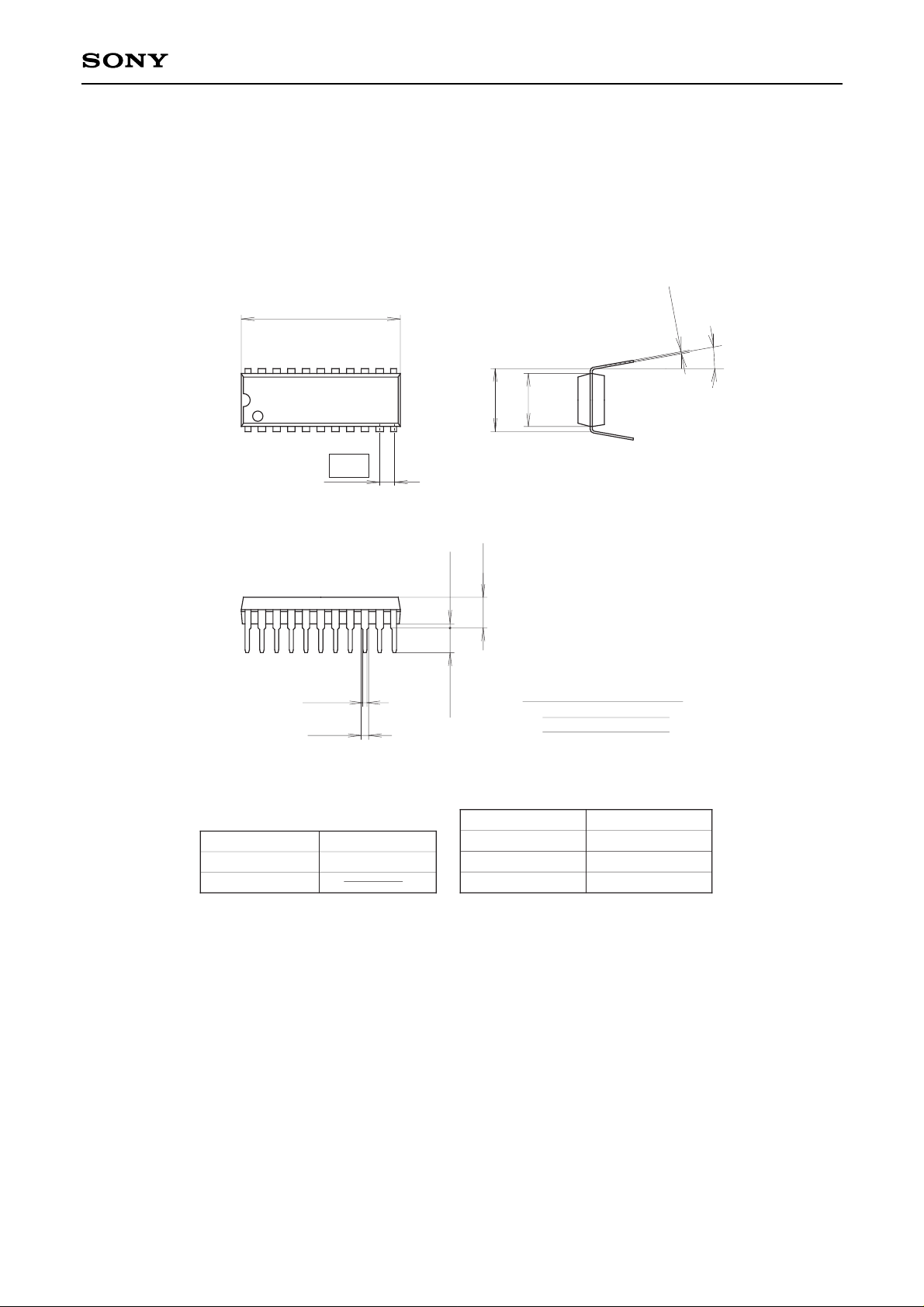
Package Outline Unit : mm
+ 0.4
19.2 – 0.1
CXA2016S
22PIN SDIP (PLASTIC)
22
1
SONY CODE
EIAJ CODE
JEDEC CODE
1.778
0.5 ± 0.1
+ 0.15
0.9 – 0.1
SDIP-22P-01
SDIP022-P-0300
12
0° to 15°
11
Two kinds of package surface:
1.All mat surface type.
2.All mirror surface type.
PACKAGE STRUCTURE
MOLDING COMPOUND
LEAD TREATMENT
LEAD MATERIAL
PACKAGE MASS
EPOXY RESIN
SOLDER PLATING
COPPER ALLOY
0.95g
—12—
 Loading...