

Page 1
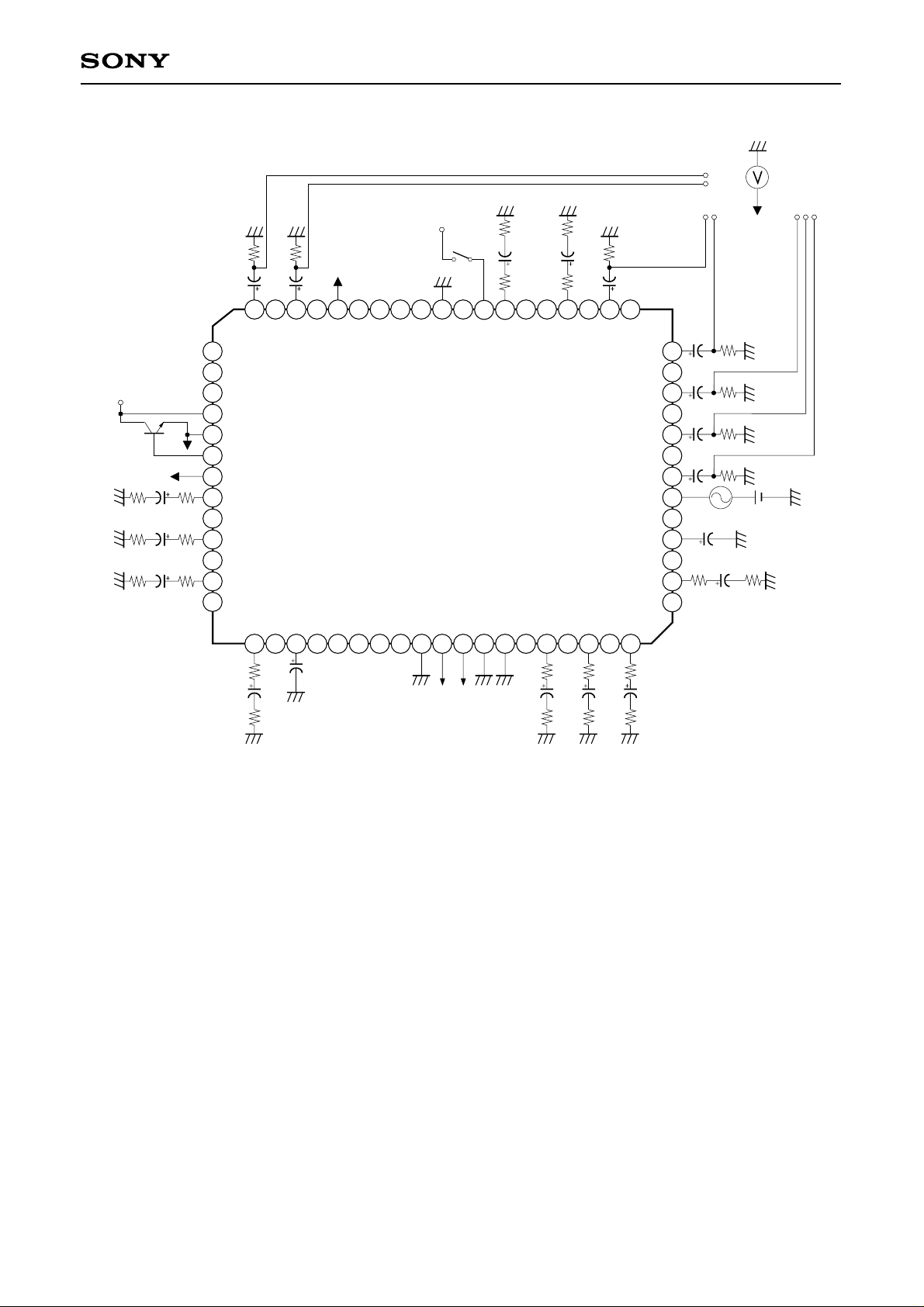
CXA2078Q
I2C Bus-Compatible Audio/Video Switc h with Electronic Volume
Description
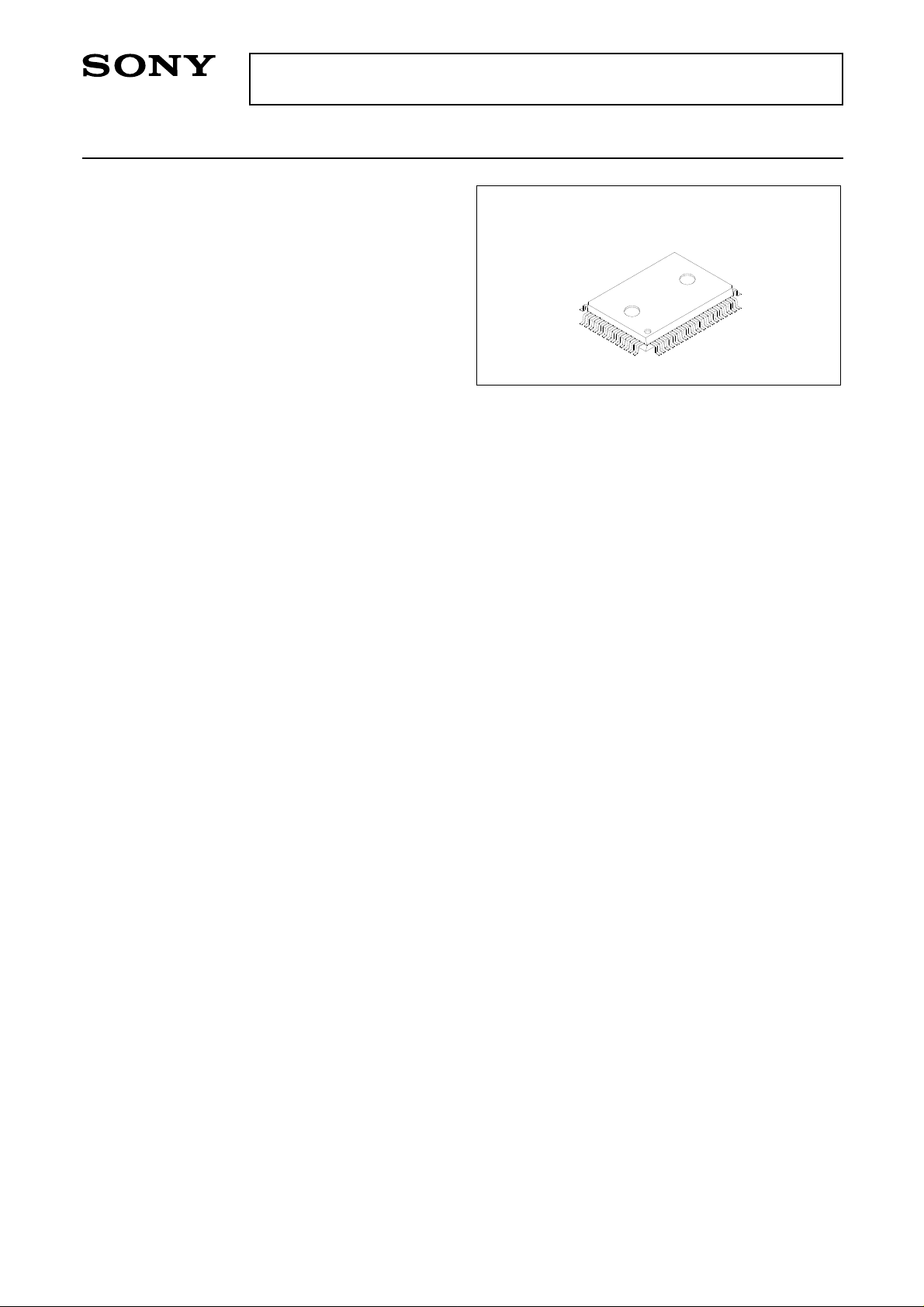
The CXA2078Q is an I2C programmable audio,
video switch designed for set top box applications. It
interfaces from digital encoder sources to TV, VCR
and auxilliary scart connectors.
Features
• 3 scart independent audio/video switching (TV, VCR,
AUX)
• 0 to –63dB volume control with click noise reduction
• 5 stereo audio inputs
• I2C control with two address setting
• Scart Function Switching input and output
• Scart Fast Blanking for OSD
• RF modulator output with Y/C mix option
• On-chip +12V to +9V voltage regulator
• 4 logic outputs
64 pin QFP (Plastic)
Applications
Audio/Video switch featuring I2C bus compatibility
for set top box
Structure
Bipolar silicon monolithic IC
Absolute Maximum Ratings
• Supply voltage VCC 12 V
• Operating temperature Topr –20 to +75 °C
• Storage temperature Tstg –65 to +150 °C
• Allowable power dissipation
PD 500 mW
Operating Conditions
• Supply voltage +10.7 to +12 V
• Operating voltage 9 ± 0.5 V
Sony reserves the right to change products and specifications without prior notice. This information does not convey any license by
any implication or otherwise under any patents or other right. Application circuits shown, if any, are typical examples illustrating the
operation of the devices. Sony cannot assume responsibility for any problems arising out of the use of these circuits.
– 1 –
E97843-PS
Page 2
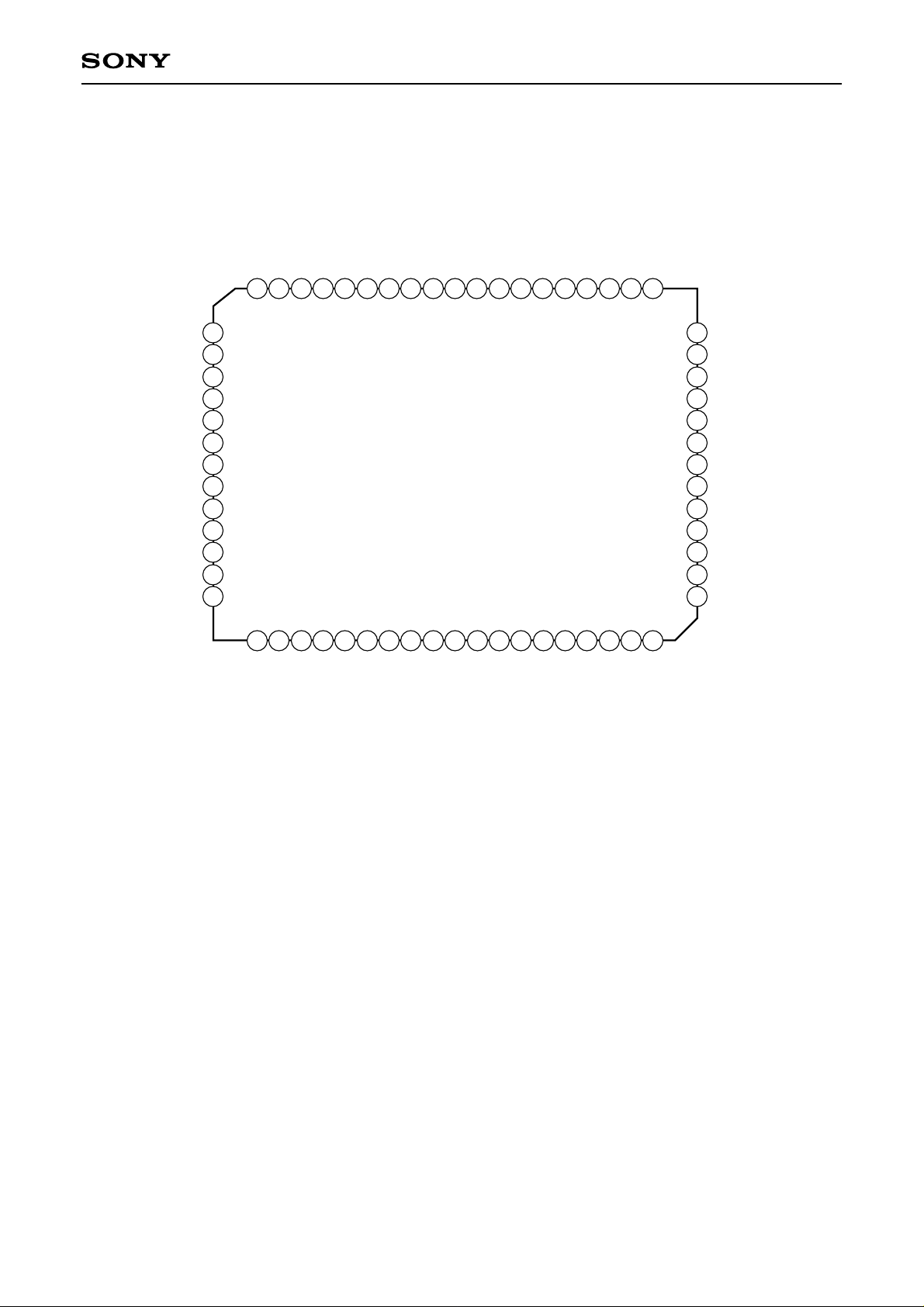
Pin Configuration
CXA2078Q
CC
VOUT2
FBLK_OUT
VOUT1
CC_12V
V
VREG_9V
VREG_BASE
VIDEO_V
CC
RIN5
FBLK_IN2
LIN5
VIN1
RIN1
VIN3
52
53
54
55
56
57
58
59
60
61
62
63
64
51
1
RTV
50
2
LIN1
LTV
VOUT3
49
48
4
3
VIN5
BIAS_VIDEO
DIG_V
VOUT4
47
5
VIN9
FNC_VCR
LOG_1
46
6
VIN6
LOG_3
LOG_2
45
44
8
7
VIN10
FNC_AUX
DIG_GND
LOG_4
43
41
42
9
10
11
SCL
VIDEO_GND
FBLK_IN1
LIN4
HW MUTE
40
39
13
12
SDA
ADR
AUDIO_GND
FNC_TVA
37
38
14
15
VIN7
TRAP
RIN4
FNC_TVB
35
36
17
16
LIN2
RIN2
VIN11
MONO
34
18
VIN2
VOUT8
33
19
RIN3
32
ROUT1
31
VOUT5
30
LOUT1
29
VOUT6
28
ROUT2
27
VOUT7
26
LOUT2
25
AUDIO_V
24
VIN12
23
BIAS_AUDIO
22
VIN8
21
LIN3
20
VIN4
CC
– 2 –
Page 3
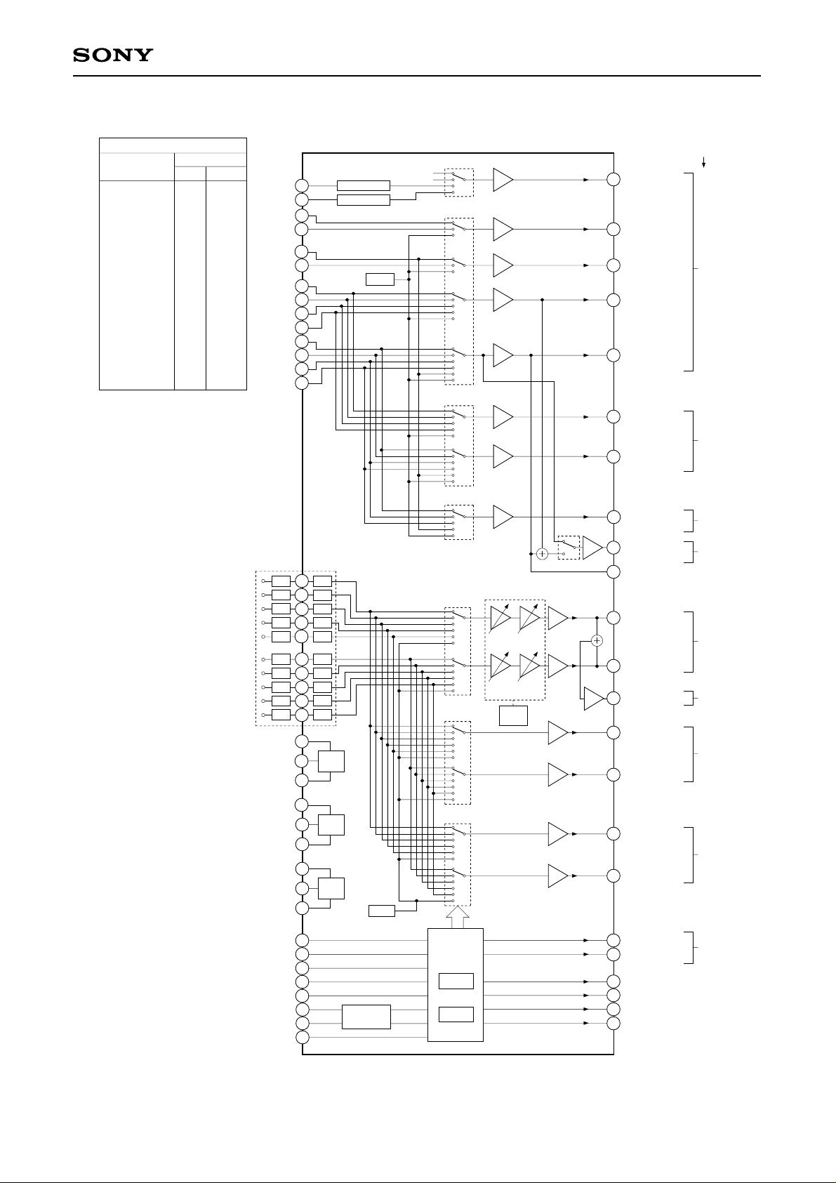
Block Diagram
CXA2078Q
TYPICAL CONFIGURATION
SOURCE
AUX
ENC
DIGITAL (OSD)
AUX
DIGITAL (OSD)
AUX
DIGITAL (OSD)
DIGITAL (NO OSD)
VCR
AUX
DIGITAL (OSD)
DIGITAL (NO OSD)
VCR
AUX
(OSD = On-Screen Display)
MODE1 MODE2
BLUE
BLUE
GREEN
GREEN
RED
RED
CVBS
CVBS
CVBS
CVBS
OUTPUT
CVBS
CHROMA
CHROMA
CHROMA
CHROMA
LUMA
LUMA
LUMA
LUMA
FBLK_IN1
FBLK_IN2
VIN10
VIN11
VIN12
RIN1
RIN2
RIN3
RIN4
RIN5
LIN1
LIN2
LIN3
LIN4
LIN5
V
CC_12V
VREG_BASE
VREG_9V
VIN1
VIN2
VIN3
VIN4
VIN5
VIN6
VIN7
VIN8
VIN9
41
60
62
18
64
20
2
6
14
22
4
8
16
24
6k
63
6k
15
6k
19
6k
36
6k
59
6k
1
6k
17
6k
21
6k
39
6k
61
55
57
56
Comparator
Comparator
Mute
BIAS
Input attenuation = 6dB
with 6k external resistor.
Att.
Att.
Att.
Att.
Att.
Att.
Att.
Att.
Att.
Att.
9V
REG
FBLK_SW
5V
0V
VIDEO
SWITCH1 (TV)
VIDEO
SWITCH2 (VCR)
VIDEO
SWITCH3 (AUX)
AUDIO
SWITCH1 (TV)
AUDIO
SWITCH2 (VCR)
× 2
× 2
× 2
× 2
× 2
× 2
× 2
Y/C MIXER
VOLUME CONTROL
& MUTE
8dB
1dB
step
step
8dB
1dB
step
step
Z.C.D
Logic
MIX_SW
× 2
× 2
× 2
× 2
× 2
53
FBLK_OUT
VOUT1
54
(BLUE)
52
VOUT2
(GREEN)
50
VOUT3
(RED/CHROMA)
VOUT4
48
(CVBS/LUMA)
31
VOUT5
(CHROMA)
VOUT6
29
(CVBS/LUMA)
VOUT7
27
(CVBS)
VOUT8
33
(CVBS)
35
TRAP
51
RTV
49
LTV
34
MONO
32
ROUT1
30
LOUT1
TYPICAL LOAD
TV
VCR
AUX
RF MOD
TV
RF MOD
VCR
VIDEO_V
BIAS_VIDEO
VIDEO_GND
AUDIO_V
BIAS_AUDIO
AUDIO_GND
DIG_V
DIG_GND
SDA
SCL
ADR
FNC_VCR
FNC_AUX
HW MUTE
58
CC
CC
CC
4.05V
BIAS
3
1
9
25
4.5V
BIAS
23
2
13
47
42
11
10
12
5
7
40
BIAS
4.5V
MONITOR
Mute
AUDIO
SWITCH3 (AUX)
I2C
INTERFACE
LOGIC
P.O.D
× 2
× 2
28
26
38
37
46
45
44
43
ROUT2
LOUT2
FNC_TVA
FNC_TVB
LOG_1
LOG_2
LOG_3
LOG_4
AUX
TV
– 3 –
Page 4
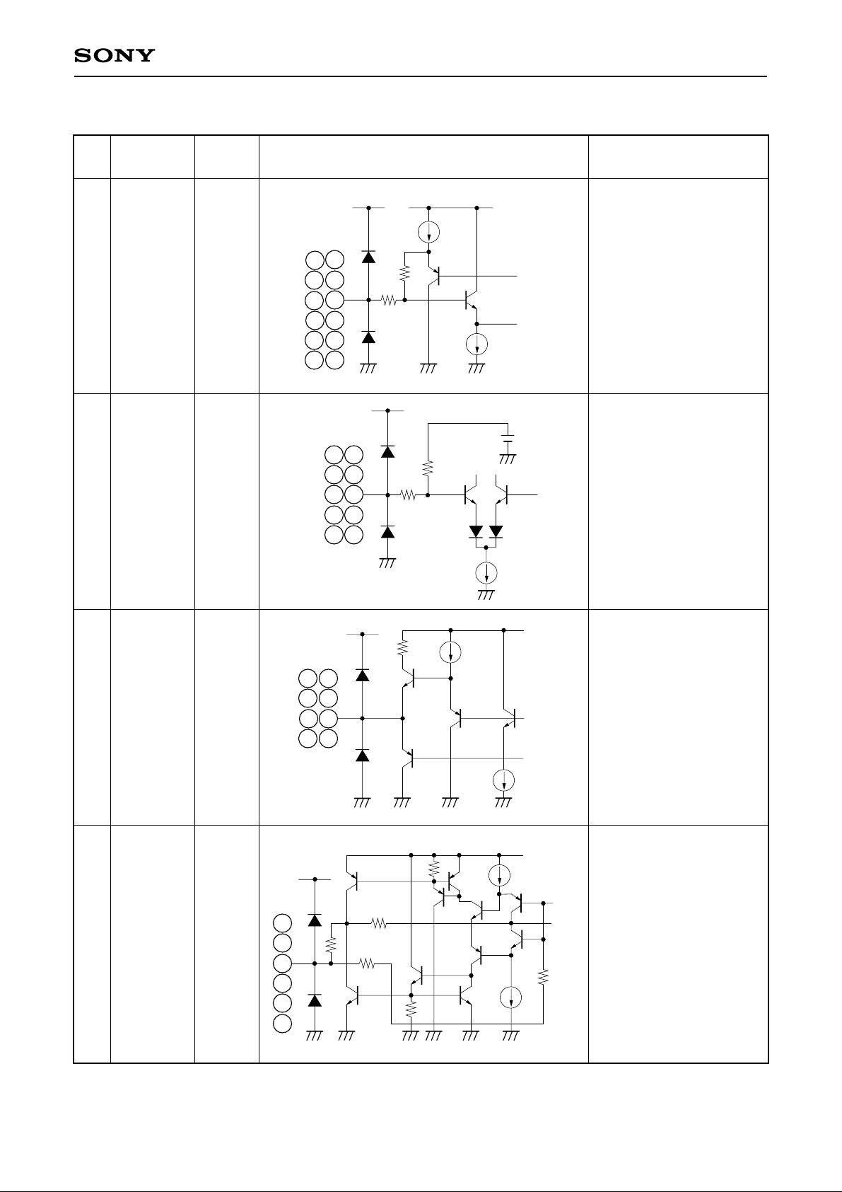
Pin Description
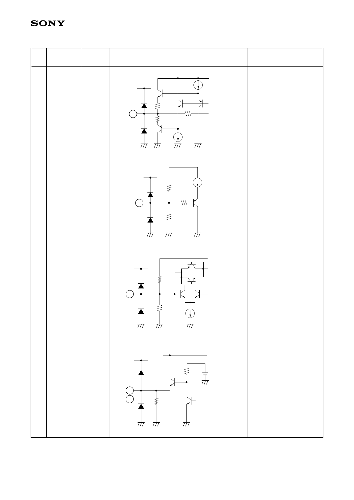
CXA2078Q
Pin
No.
62
18
64
20
2
6
14
22
4
8
16
24
63
15
19
36
59
1
17
21
39
61
Symbol
VIN1
VIN2
VIN3
VIN4
VIN5
VIN6
VIN7
VIN8
VIN9
VIN10
VIN11
VIN12
RIN1
RIN2
RIN3
RIN4
RIN5
LIN1
LIN2
LIN3
LIN4
LIN5
Pin
voltage
4.6V
4.5V
VCC = 12V
14
62
18
22
4
64
8
20
2
16
6
24
VCC = 12V
63
15
19
36
59
Equivalent circuit Description
VCC = 9V
14µA
120k
Video signal inputs.
Input impedance typically
120kΩ.
Audio signal inputs.
Input impedance typically
60kΩ.
17
61
21
39
147
60µA
4.5V
1
33k
27k
7µA
54
52
50
48
31
29
27
33
51
32
28
49
30
26
VOUT1
VOUT2
VOUT3
VOUT4
VOUT5
VOUT6
VOUT7
VOUT8
RTV
ROUT1
ROUT2
LTV
LOUT1
LOUT2
3.9V
4.5V
VCC = 12V
48
VCC = 12V
51
32
28
49
30
26
54
52
50
31
29
27
33
55
20k
200
22k
VCC = 9V
140µF
Video signal outputs.
280µA
VCC = 9V
33µA
Audio signal outputs.
20k
33µA
– 4 –
Page 5
CXA2078Q
Pin
No.
34
3
Symbol
MONO
BIAS_
VIDEO
Pin
voltage
4.5V
3.9V
VCC = 12V
34
VCC = 12V
3
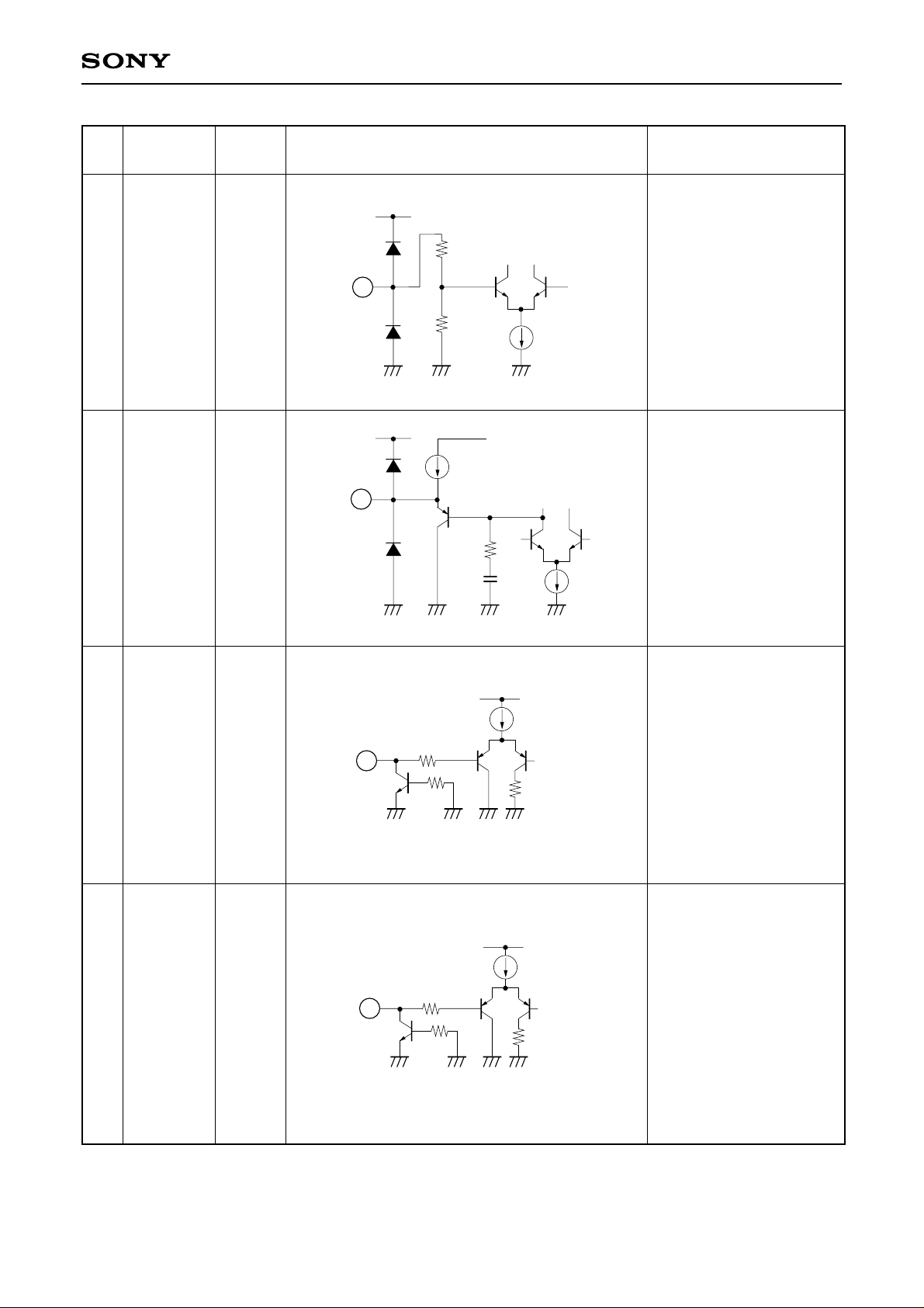
Equivalent circuit Description
VCC = 9V
75µA
200
Audio mono signal output.
11k
20k
75µA
VCC = 9V
14µA
Reference Bias for video
200
circuit.
200
9k
Connected to GND with
capacitor.
23
37
38
BIAS_
AUDIO
FNC_TVB
FNC_TVA
4.5V
—
VCC = 12V
23
VCC = 12V
37
38
20k
20k
20k
40k
7µA
VCC = 9V
VCC = 9V
2.7V
Reference Bias for audio
circuit.
Connected to GND with
capacitor.
I2C controlled output
giving 0/2V.
Maximum load current
= 800µA
– 5 –
Page 6
CXA2078Q
Pin
No.
56
57
Symbol
VREG_9V
VREG_
BASE
Pin
voltage
9V
9.7V
56
VCC = 12V
57
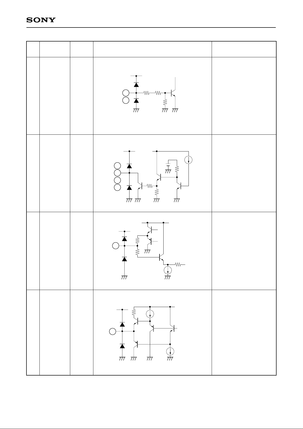
Equivalent circuit Description
VCC = 12V
77.7k
Pin connected to emitter
of external regulator
transistor.
13.5k
1mA
120µA
VCC = 12V
Connection to base of
external regulator
413
15p
120µA
transistor.
10
11
SCL
SDA
—
—
10
11
4k
4k
10k
4.5k
40µA
40µA
V
CC = 9V
40k
VCC = 9V
40k
I2C Clock Input.
VIL = 1.5V (max)
VIH = 3.0V (min)
I2C Data input/output.
VIL = 1.5V (max)
VIH = 3.0V (min)
VOL = 0.4V (max)
– 6 –
Page 7
CXA2078Q
Pin
No.
12
40
43
44
45
46
Symbol
ADR
HW MUTE
LOG_4
LOG_3
LOG_2
LOG_1
Pin
voltage
—
—
12
40
VCC = 12V
43
44
45
46
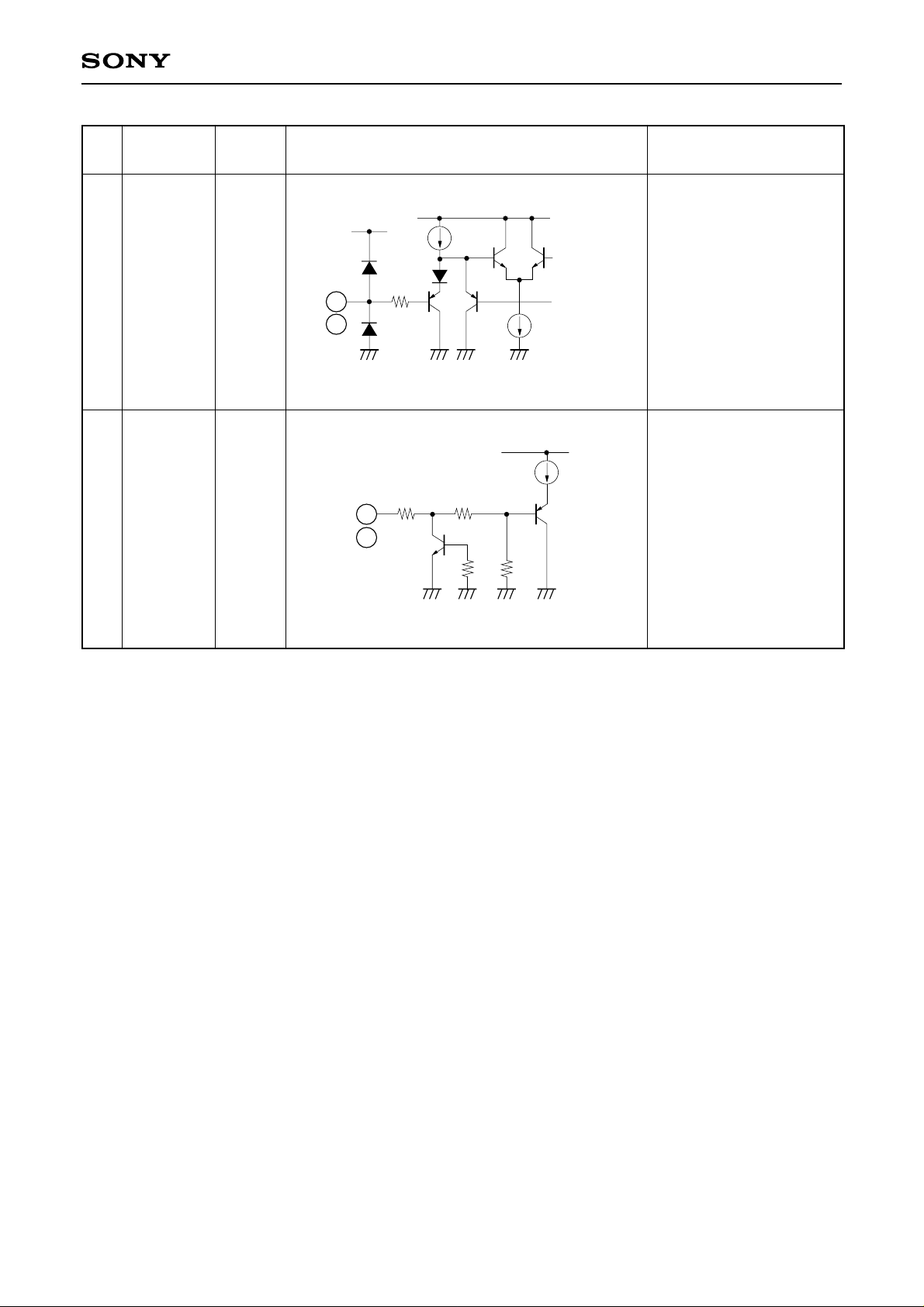
Equivalent circuit Description
HW MUTE: This pin is
VCC = 12V
active high > 2.5V.
When high, audio outputs
72k
147
RTV, LTV and MONO are
muted.
28k
ADR: Selects the I2C
address for the IC.
< 1.5V = Low Add = 90H
> 2.5V = High Add = 92H
VCC = 9V
40k
8µA
Open collector logic Pins.
3V
Maximum current sink
= 1mA
4.5k
7.5k
35
53
TRAP
FBLK_
OUT
3.9V
—
VCC = 12V
35
VCC = 12V
53
1k
147
100
100µA
VCC = 9V
470µA
VCC = 9V
100µA
Connection to external
trap circuit.
Trap components should
be kept as close as
possible to this pin.
Fast Blank output set by
I2C, FBLK_IN1 or
FBLK_IN2.
High = 5.1V
Low = 1.2V
Connected to external
emitter follower.
Maximum load current
= 800µA
– 7 –
Page 8
CXA2078Q
Pin
No.
41
60
5
7
Symbol
FBLK_IN1
FBLK_IN2
FNC_VCR
FNC_AUX
Pin
voltage
—
—
VCC = 12V
41
60
5
7
Equivalent circuit Description
V
CC = 9V
50µA
Fast Blank inputs.
147
Low = < 0.4V
High = > 1.0, < 3.0
90µA
VCC = 9V
80µA
50k
50k
Function switching input
(Scart pin 8).
Typical levels
= 0V/6V/12V
10k
100k
– 8 –
Page 9

CXA2078Q
Electrical Characteristics
Absolute Maximum Ratings
Supply Voltage Vcc_12V 12 V
Operating Conditions
• Supply Voltage Vcc_12V 12 to 10.7 V
• Voltage Regulation Vreg_9V 9 ± 0.45 V (from 12V supply)
• Operating Voltage Video_Vcc, Dig_Vcc, 9 ± 0.5 V
Audio_Vcc 9 ± 0.5 V
FNC_TVA (pin 38) and FNC_TVB (pin 39) are static sensitive.
Precaution should be taken (note 8 in "Notes on Operation").
Operation of the CXA2078Q using a 9V supply connected directly to the VCC_12V, Video_VCC, AUDIO_VCC
and Dig_VCC pins is possible but not recommended. (The unused on-chip voltage regulator is then forced to
have pins Vreg_base and Vreg_9V floating.)
– 9 –
Page 10
CXA2078Q
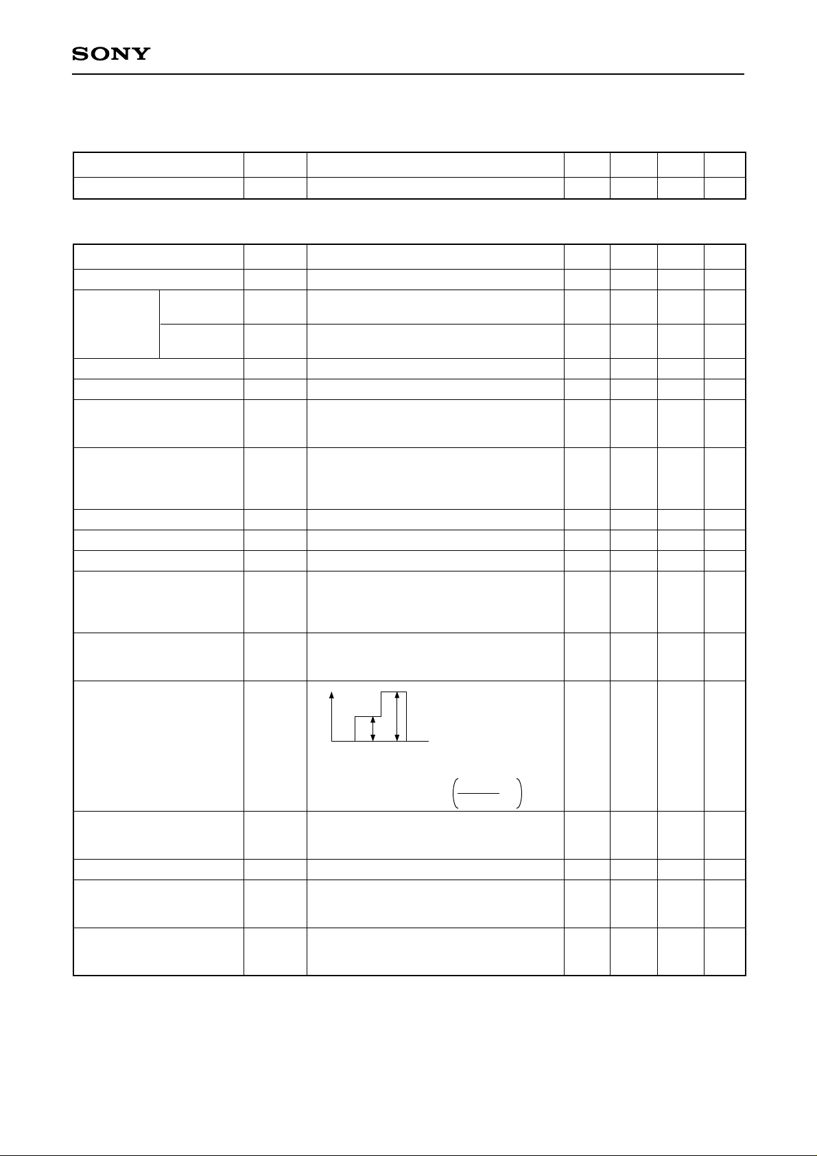
Electrical Characteristics
Nominal conditions (Ta = 25°C)
Item Symbol Conditions Min. Typ. Max. Unit
Current Consumption ICC 30 50 70 mA
VCC_12V = 12V, No signal, no load
Video system Nominal conditions (Ta = 25°C, Vcc_12V = 12V)
Item Symbol Conditions Min. Typ. Max. Unit
Input pin voltage
Output pin
voltage
Vout1 – 8
Vout8 (mix)
Gain (except Y/C mixer)
Gain of Y/C mixer
Bandwidth
(except Y/C mixer)
VVPin
VVPout
VVPoutm
GVv
GVYC
fV3dB
No signal, no load (Fig.1)
No signal,no load,Y/C mix inactive
(Fig.1)
No signal, no load, Y/C mix active
(Fig.1)
f = 200kHz, 0.3Vp-p input (Fig.2)
f = 200kHz, 0.3Vp-p input (Fig.2)
0.3Vp-p input, frequency where output
level is –3dB with 200kHz serving as
0dB (Fig. 2)
4.3
3.6
3.5
5.5
5.4
15
4.6
3.9
3.8
6.0
6.0
20
4.9
4.2
4.2
6.5
6.4
V
V
V
dB
dB
MHz
0.3Vp-p input, frequency where output
Bandwidth of Y/C Mixer
fYC3dB
level is –3dB with 200kHz serving as
0dB. No trap connected. (See note below)
7
15
—
MHz
(Fig.2)
Input dynamic range
Output dynamic range
Cross talk
VDRVI
VDRVO
Vctv
200kHz input (Fig.2)
200kHz, 2.5Vp-p input (Fig.2)
f = 4.43MHz, 1Vp-p input (Fig.2)
2.5
5.0
—
—
—
—
—
—
–50
Vp-p
Vp-p
dB
Ratio of 0.7Vp-p white video signal to
S/N ratio
S/NV
black line noise. Weighted using
CCIR 567. HPF @ 5kHz,
—
72
—
dB
LPF @ 5MHz. (Fig.2)
1Vrms 1kHz input through 56kΩ.
Input Impedance
ZinV
Attenuation measured to calculate ZinV
94
120
kΩ
(Fig.3)
V2
V1
(Fig.4)
–3
–0.4
+3
%
Non-linearity
Input/V
Lin
V1 = Pin Voltage +0.5V
V2 = Pin Voltage +1V
At output, non-linearity = –1 × 100
V2
V1 × 2
1.7Vp-p 5-step modulated staircase.
Differential Gain
DG
(Chroma and Burst are 150mVp-p
1.5
%
4.43MHz) (Fig.2)
Differential Phase
DP
as above. (Fig.2)
1
Deg
Percentage reduction in sync pulse
Sync crush
SC
(0.4Vp-p), with tip at –1.2V input offset.
0.2
3
%
(Fig.4)
Delay of Luma over
Chroma through mixer
tcld
0.4Vp-p square wave input. Input to
output edge delay measured. No trap.
(Fig.2)
15
40
ns
Note) Input output path from Vin9 – 12 to Vout 8 through mixer has BW reduced by external stray capacitance
on TRAP pin.
– 10 –
Page 11
CXA2078Q
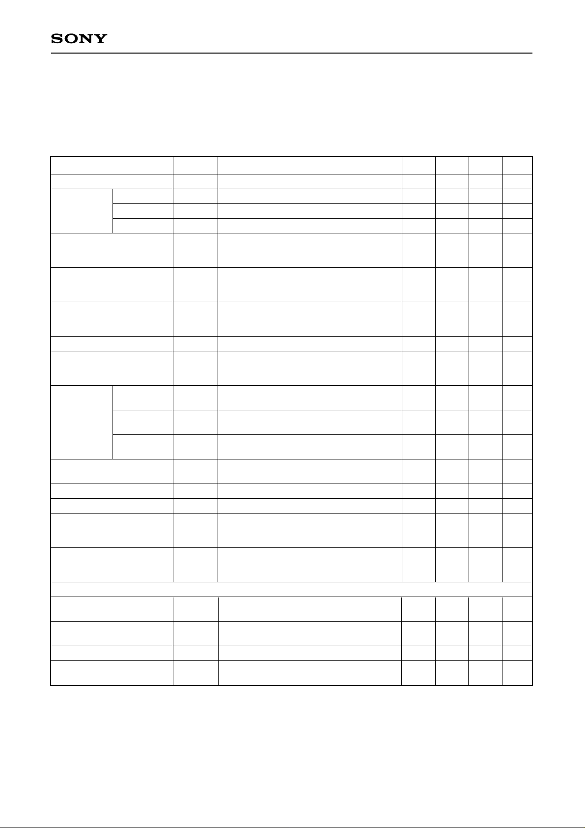
Electrical Characteristics
Audio system
Unless otherwise stated: input coupling capacitor 1µF in series with 6kΩ resistor; output coupling capacitor of
10µF; load of 10kΩ. Nominal conditions (Ta = 25°C, Vcc_12V = 12V)
Item Symbol Conditions Min. Typ. Max. Unit
Input pin voltage
R/LOUT1, 2
Gain
RTV, LTV
MONO
Audio frequency
response
VAPIN
GVA
GVATV
GVAM
FAF
No signal, no load (Fig. 5)
f = 1kHz, 1Vrms input. (Fig. 6)
f = 1kHz, 1Vrms input. (Fig. 6)
f = 1kHz, 1Vrms "stereo" input. (Fig. 6)
0.3Vp-p input. Output level at 30kHz
with 1kHz serving as 0dB. 6kΩ
removed. (Fig. 7)
4.2
–0.5
–0.65
–0.65
–0.3
4.5
0
0
0
0
4.8
+0.5
+0.35
+0.45
+0.3
V
dB
dB
dB
dB
0.3Vp-p input; frequency where output
Frequency B/W
FBWA1
level is –3dB with 1kHz serving as
—
1
—
MHz
0dB. 6kΩ removed. No load (Fig. 7)
f = 1kHz, 0.5Vrms, unweighted
Distortion
THD
response; LPF @400Hz,
—
0.004
0.2
%
HPF @ 80KHz. (Fig. 6)
Input Dynamic Range
Cross talk
(Channel separation)
R/LOUT1, 2
Ripple
rejection
RTV, LTV
MONO
DC Offset -R/Lout1, 2
Input impedance
Output Impedance
VdA
VctA
RRA
RRATV
RRAM
Voff
Zin
Zout
f = 1kHz (Fig. 6)
f = 1kHz, 1Vrms input on one input,
measure on any other audio output.
(Fig.6)
f = 100Hz, 0.3Vp-p applied to Vcc_aud
(Fig. 8)
f = 100Hz, 0.3Vp-p applied to Vcc_aud
(Fig. 8)
f = 100Hz, 0.3Vp-p applied to Vcc_aud
(Fig. 8)
Offset voltage between any audio input
and R/Lout1, 2 (Fig. 5)
(excluding series external 6kΩ)
(excluding any external series resistor)
2
—
—
—
—
–30
48
—
—
–88
–62
–75
–44
+2
60
10
—
–76
—
—
—
+30
72
—
Vrms
dB
dB
dB
dB
mV
kΩ
Ω
f = 1kHz, 1Vrms input to two channels.
Phase Difference
Vpda
Phase difference of stereo output
—
0.05
—
Deg
measured
S/N ratio
S/NA
f = 1kHz, 1Vrms input (at maximum
volume).
72
95
—
dB
HPF @ 20Hz, LPF @ 20kHz. (Fig. 6)
Electronic Volume Control
Fine volume attenuation
step
Coarse volume
attenuation step
Mute
DC Offset -RTV, LTV
AEVC
AEVF
Amute
VoffTV
f = 1kHz, 0.5Vrms input. Set by I2C
(Fig.6)
f = 1kHz, 0.5Vrms input. Set by I2C
(Fig.6)
f = 1kHz, 1Vrms input. (Fig.6)
Offset voltage between any audio input
and RTV, LTV outputs (Fig.5)
0.6
7.5
–30
1
8
>80
+2
1.4
8.5
+30
dB
dB
dB
mV
– 11 –
Page 12

CXA2078Q
+12V
BC547B
+12V
BC547B
+12V
BC547B
+9V
1k
1k
+9V
52
53
55
56
57
58
59
60
61
62
63
64
54
51
18
34
33
19
+12V
BC547B
1k
32
31
30
29
28
27
26
25
24
23
22
21
20
Measurement
Point
1k
BC547B
1k
BC547B
1k
BC547B
+9V
22µF
+12V
+12V
+12V
BC547B
+9V
48
47
5
4
+12V
46
6
BC547B
1k
45
44
7
47µH
25pF
1k
Trap
Switch
SW1
35
42
10
41
11
40
12
43
9
8
39
13
38
14
37
15
36
16
17
+12V
1k
49
50
1
2
3
SCL SDA
47µF
Measurement
Point
Fig. 1. Video system (d.c.test)
Notes) 1. All +9V supplies de-coupled close to supply pins, 25, 47, 58 with 10nF ceramic capacitor.
2. All video outputs are loaded with emitter follower during tests.
3. Voltage measurements carried out with a high input impedance DVM. Typically 10GΩ.
– 12 –
Page 13
CXA2078Q
+12V
BC547B
+12V
BC547B
+12V
BC547B
+9V
75
75
1k
1k
+9V
2.2µF
2.2µF
52
53
54
55
56
57
58
59
60
61
62
63
64
51
1
2.2µF
75
50
2
+12V
1k
49
3
47µF
BC547B
+9V
48
47
5
4
75 2.2µF
+12V
46
6
BC547B
1k
45
44
7
2.2µF
75
75 2.2µF
8
43
9
10
SCL SDA
4142
11
12
40
39
13
38
14
47µH
25pF
Trap
Switch
SW1
37
15
75 2.2µF
36
16
1k
17
35
+12V
Measurement
1k
1k
1k
+9V
75
75
75
Point
BC547B
BC547B
BC547B
22µF
+12V
+12V
+12V
BC547B
1k
33
34
32
31
30
29
28
27
26
25
24
2.2µF
23
22
2.2µF
21
20
2.2µF
19
18
2.2µF
75
75 2.2µF
Input
Signal
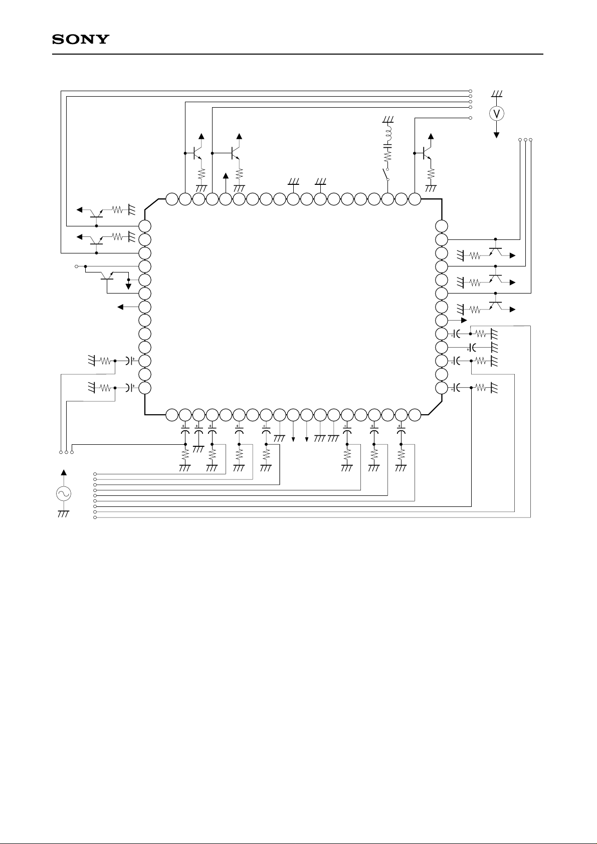
Fig. 2. Video system (gain, dynamic range, bandwidth, differential gain, differential phase,
crosstalk, signal to noise, Luma-Chroma delay)
Signal applied to Pins 2, 4, 6, 8, 14, 16, 18, 20, 22, 24, 62, 64
Output Signal Measured from pins 27, 29, 31, 33, 48, 50, 52, 54
Notes) 1. All +9V supplies de-coupled close to supply pins, 25, 47, 58 with 10nF ceramic capacitor.
2. For tests requiring video measuring equipment with 75Ω input impedance, an external video line
driver or buffer is used.
3. For bandwidth tests through Y/C mixer, the trap circuit is switched out using SW1.
4. All video outputs are loaded with emitter follower during tests.
5. For Luma and Chroma input to output delay, measure signal at the I.C. pins.
– 13 –
Page 14
51
50
49
48
+9V
47
46
45
44
43
42
41
40
39
38
37
36
35
34
CXA2078Q
33
+12V
BC547B
56k
56k
56k
+9V
+9V
2.2µF
2.2µF
2.2µF
52
53
54
55
56
57
58
59
60
61
62
63
64
1
2
47µF
32
31
30
29
28
27
26
25
24
23
22
21
20
6
5
4
3
2.2µF
56k
7
2.2µF
56k
8
2.2µF
9
10
SCL SDA
56k
11
12
13
14
15
16
2.2µF
56k
17
2.2µF
56k
18
19
2.2µF
56k
+9V
22µF
2.2µF
56k
2.2µF
56k
2.2µF
56k
Signal
Input
Measurement
Point
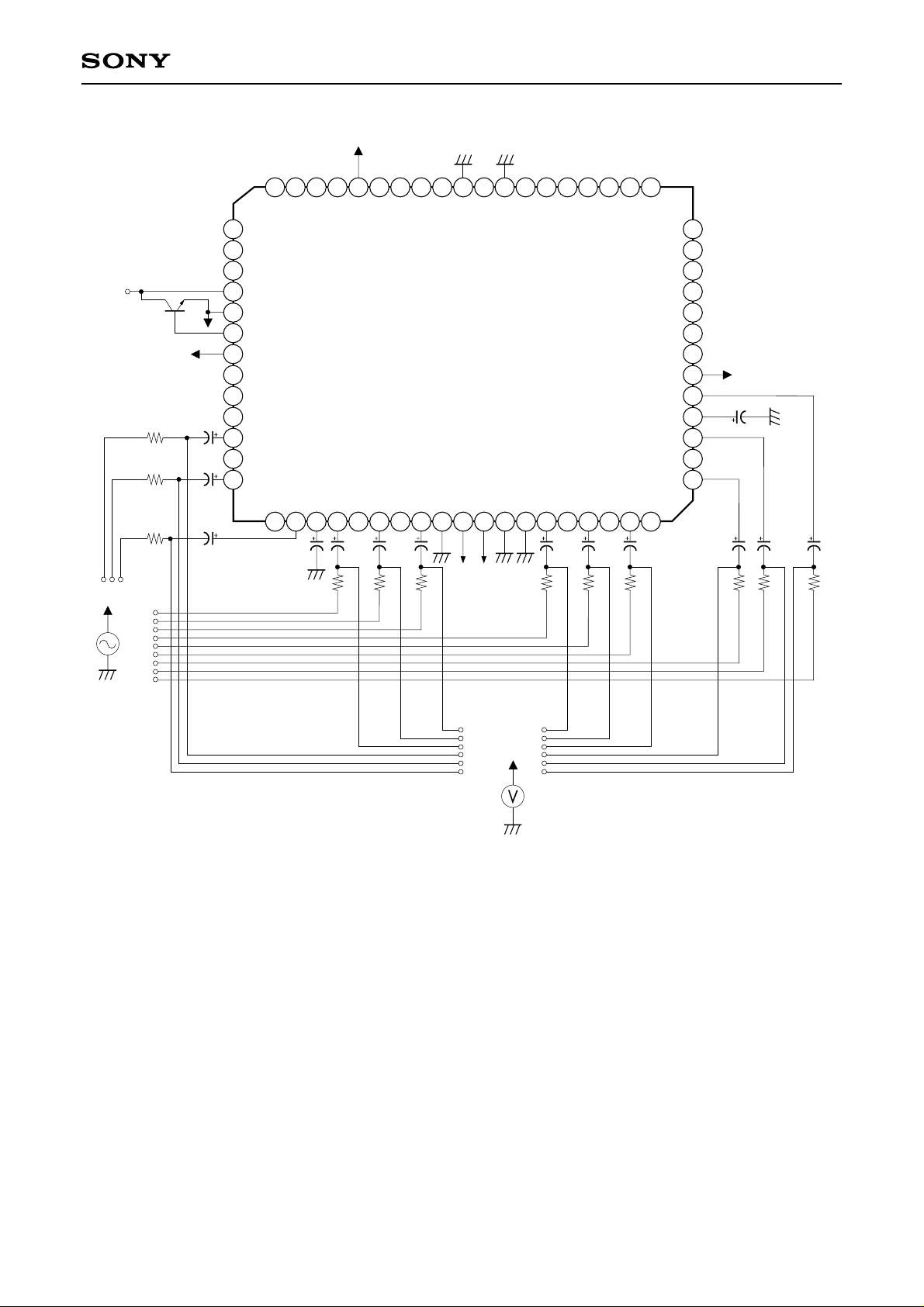
Fig. 3. Video system (input impedance)
Signal applied and measured from pins, 2, 4, 6, 8, 14, 16, 18, 20, 22, 24, 62, 64
Notes) 1. All +9V supplies de-coupled close to supply pins, 25, 47, 58 with 10nF ceramic capacitor.
2. Voltage measurements carried out with a high input impedance DVM. Typically 10GΩ.
– 14 –
Page 15
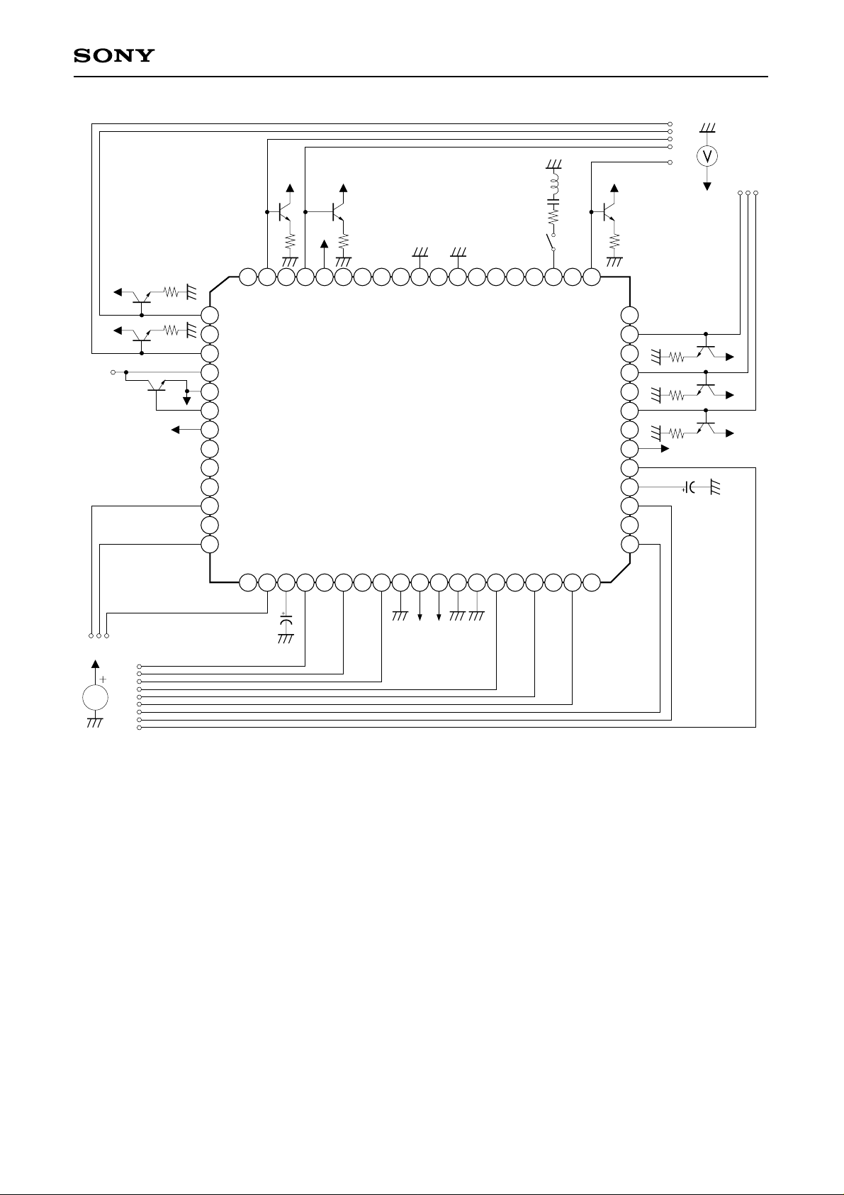
CXA2078Q
+12V
BC547B
+12V
BC547B
+12V
BC547B
+9V
1k
1k
+9V
52
53
54
55
56
57
58
59
60
62
63
64
61
51
34
18
33
19
+12V
BC547B
1k
32
31
30
29
28
27
26
25
24
23
22
21
20
Measurement
Point
1k
BC547B
1k
BC547B
1k
BC547B
+9V
22µF
+12V
+12V
+12V
BC547B
+9V
48
47
5
4
+12V
46
6
BC547B
1k
45
44
7
47µH
25pF
1k
Trap
Switch
SW1
35
39
13
38
14
37
15
16
36
17
10
40
4142
12
11
43
9
8
+12V
1k
49
50
1
2
3
SCL SDA
47µF
PSU
Input
Signal
Fig. 4. Video system (linearity, sync crush)
Signal applied to Pins, 2, 4, 6, 8, 14, 16, 18, 20, 22, 24, 62, 64
Output Signal Measured from pins 27, 29, 31, 33, 48, 50, 52, 54
Notes) 1. All +9V supplies de-coupled close to supply pins, 25, 47, 58 with 10nF ceramic capacitor.
2. All video outputs are loaded with emitter follower during tests.
– 15 –
Page 16
51
50
49
48
+9V
47
46
45
44
HW
mute
43
+9V
42
SW1
41
40
39
38
37
36
35
34
CXA2078Q
Output
Measurement
Point
33
+12V
BC547B
+9V
+9V
52
53
55
56
59
61
62
63
64
54
57
58
60
32
31
30
29
28
27
26
25
+9V
24
22µF
23
22
21
20
6
1
2
5
4
3
47µF
9
10
8
7
SCL SDA
11
12
13
14
15
16
17
18
19
Input
Measurement
Point
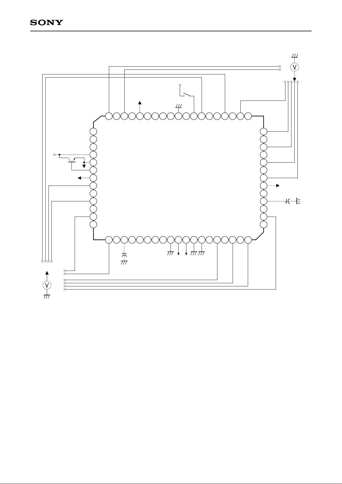
Fig. 5. Audio system (d.c. tests)
Notes) 1. All +9V supplies de-coupled close to supply pins, 25, 47, 58 with 10nF ceramic capacitor.
2. Voltage measurements carried out with a high input impedance DVM. Typically 10GΩ.
– 16 –
Page 17
CXA2078Q
+12V
BC547B
600
600
600
1µF
1µF
1µF
+9V
+9V
6k
6k
6k
54
55
56
57
58
59
60
62
63
64
52
53
61
1µF
600
6k
10µF
10k
51
1
50
+9V
HW
SW1
45
mute
43
44
8
7
42
9
10
SCL SDA
41
11
10k
+9V
10µF
48
4
47µF
47
46
6
5
49
2
3
600
1µF
6k
40
38
39
13
12
14
1µF 1µF 1µF
6006k6006k600
37
15
36
16
35
17
600
1µF
6k
34
18
10k
10µF
33
32
31
30
29
28
27
26
25
24
23
22
21
20
19
6k
10µF
10µF
10µF
10µF
22µF
6k
Measurement
Point
10k
10k
10k
10k
+9V
600
1µF
Input
Signal
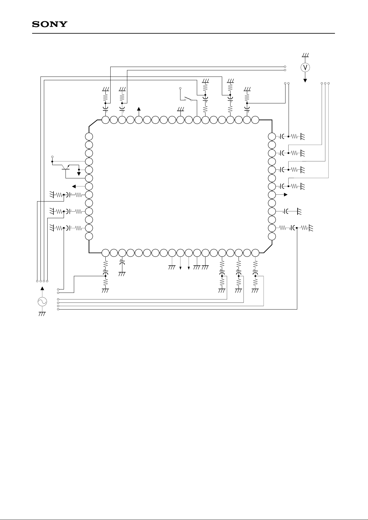
Fig. 6. Audio system (gain, dynamic range, Signal to noise, Crosstalk, Distortion, Volume control)
Signal applied to Pins, 63, 1, 59, 61, 15, 17, 19, 21, 36, 39
Output Signal Measured from pins 26, 28, 30, 32, 34, 49, 51
Notes) 1. All +9V supplies de-coupled close to supply pins, 25, 47, 58 with 10nF ceramic capacitor.
2. When muting audio using Hardware mute, SW1 is closed.
– 17 –
Page 18
CXA2078Q
+12V
BC547B
600
600
600
1µF
1µF
1µF
+9V
+9V
52
53
55
56
59
61
62
63
64
54
57
58
60
1µF
600
10µF
10k
51
1
50
+9V
HW
SW1
45
mute
43
44
8
7
42
9
10
SCL SDA
41
11
10k
+9V
10µF
48
4
47µF
47
46
6
5
49
2
3
600
1µF
40
38
39
13
12
14
1µF 1µF 1µF
600 600 600
15
37
16
36
35
17
600
1µF
34
18
10k
10µF
33
32
31
30
29
28
27
26
25
24
23
22
21
20
19
10µF
10µF
10µF
10µF
22µF
Measurement
Point
10k
10k
10k
10k
+9V
600
1µF
Input
Signal
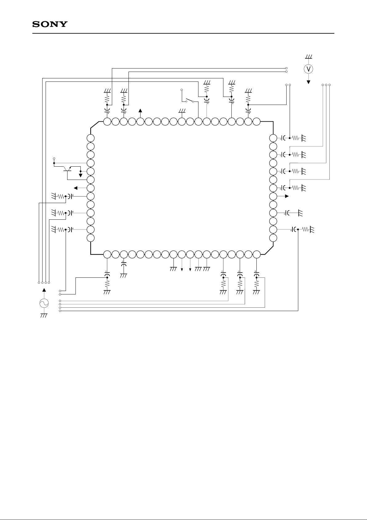
Fig. 7. Audio system (Bandwidth)
Signal applied to Pins, 63, 1, 59, 61, 15, 17, 19, 21, 36, 39
Output Signal Measured from pins 26, 28, 30, 32, 34, 49, 51
Note) All +9V supplies de-coupled close to supply pins, 25, 47, 58 with 10nF ceramic capacitor.
– 18 –
Page 19
CXA2078Q
+12V
BC547B
600
600
600
1µF
1µF
1µF
+9V
+9V
6k
6k
6k
55
56
57
58
59
60
62
63
64
52
53
54
61
1µF
600
6k
10µF
10k
51
+9V
HW
SW1
45
mute
43
44
8
7
9
10
SCL SDA
4142
12
11
10k
+9V
10µF
48
4
47µF
47
46
6
5
49
50
1
2
3
600
1µF
6k
40
38
39
13
14
1µF 1µF 1µF
6006k6006k600
37
15
36
16
35
17
600
1µF
6k
34
18
10k
10µF
33
32
31
30
29
28
27
26
25
24
23
22
21
20
19
6k
Measurement
Point
10µF
10k
10µF
10k
10µF
10k
10µF
10k
100Hz 0.3Vp-p
22µF
600
1µF
6k
+9V
Fig. 8. Audio system (Ripple Rejection)
Output Signal Measured from pins 26, 28, 30, 32, 34, 49, 51
Note) All +9V supplies de-coupled close to supply pins, 25, 47, 58 with 10nF ceramic capacitor.
– 19 –
Page 20
CXA2078Q
75
1917151311
21
20
1816141210
TO
AUDIO4_R
BC547B
50 1k
AUDIO4_L
1k
+12V
MODULATOR
1k
10k10k
HW_MUTE
75
10k10k10k
97531
864
VCR SCART
27pF
47µH
1µ
6k
2.2k2.2k
6k
1µ
2
VOUT8
33
MONO
34
TRAP
35
RIN4
36
FNC_TVB
37
FNC_TVA
38
LIN4
39
HW MUTE
40
FBLK_IN1
4142
DIG_GND
LOG_4
43
LOG_3
44
LOG_2
45
60010µ
ROUT1
32
+12V
BC547B
VOUT5
75
19
18
17
16
15
14
13
12
11
10
9
8
7
97531
864
1µ
6k
RIN3
75
0.47µ
VIN2
1µ
6k
LIN2
VIN11
1µ
6k
RIN2
VIN7
AUDIO_GND
ADR
SDA
SCL
VIDEO_GND
VIN10
0.47µ0.47µ
FNC_AUX
0.47µ
0.47µ
2
10k
10k
C
2
I
1917151311
0.47µ
VIN8
AUX SCART
75
22
21
20
6k 1µ
LIN3
21
1816141210
0.47µ
VIN4
20
75
75
BC547B
60010µ
LOUT1
31
VOUT6
30
+12V
1k
1k 1k
60010µ
29
ROUT2
28
VOUT7
27
BC547B
60010µ
LOUT2
9V_REG
4.7µ
CC
AUDIO_V
26
CXA2078Q
75 75
10nF
22µ
0.47µ
VIN12
BIAS_AUDIO
24
25
23
LOG_1
CC
10µ
10µ
BC547B
75
10
46
DIG_V
47
VOUT4
48
LTV
49
VOUT3
50
RTV
51
BC547B
75
97531
864
10k
9V_REG
+12V
75
BC547B
1917151311
21
2018161412
T. V. SCART
4.7µ 10nF
600
600
BC547B
75
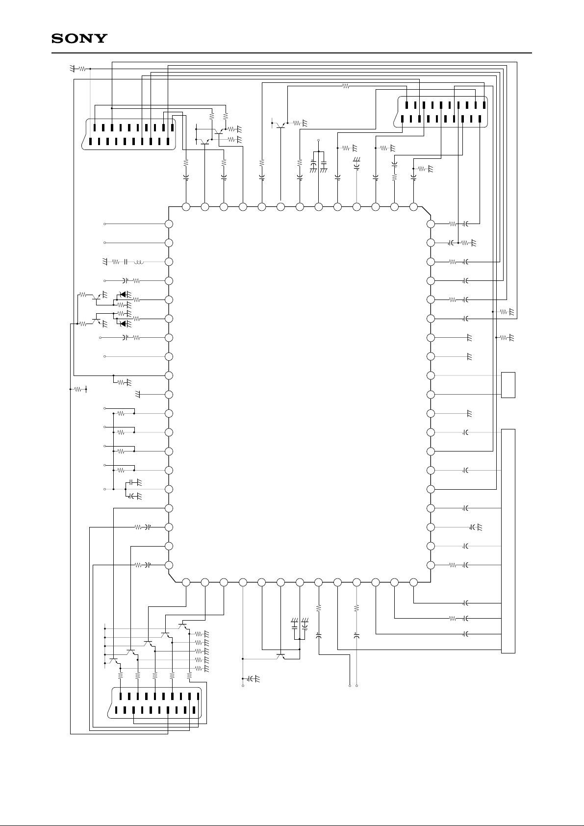
Typical Application Circuit
52
VOUT2
75
2
53
FBLK_OUT
BC547B
5×1k
54
VOUT1
CC_12V
V
+12V
55
VREG_9V
47µ
56
57
CC
VIDEO_V
VREG_BASE
10nF
BC547B
– 20 –
6
VIN6
5
FNC_VCR
4
VIN9
0.47µ
VIN5
LIN1
BIAS_VIDEO
6k
6k
47µ
0.47µ1µ
0.47µ1µ
0.47µ
ENCODER
3
2
1
61
4.7µ
6k
RIN5
60
59
LIN5
FBLK_IN2
6k
1µ
1µ
R
L
AUDIO 5
58
VIN1
63
RIN1
64
VIN3
62
Page 21

CXA2078Q
Description of operation
1. Explanation of Video Section
The video section comprises of 12 high impedance (120kΩ) inputs switched through to 8 video outputs. A
+6dB internal amplifier is connected to each output. The amplifier is required to compensate for the 6dB
attenuation which occurs at the external emitter follower stage used for driving video loads. The typical
external configuration is shown in Fig. 1-1.
A Y/C mixer can be used for mixing Luma and Chroma signals for use with an external RF modulator
connected to Vout8. The Y/C mixer is controllable via the I2C data bus. The circuit is shown in Fig. 1-2 with a
trap circuit used to give 3dB attenuation at 4.43MHz of the Luma signal.
AMP
CC = 9V
Vbias
Vout
V
CC = 12V
BC547B
beta = 250
SCART_out
75Ω
1kΩ 75Ω
SCART_in
75Ω
75Ω
0.47µ
Video_V
Switch
Vin
120kΩ
Vbias
Video element
Fig. 1-1. Video circuit element: 6dB gain amplifier with external emitter follower
R/C
CVBS/Y
6dB
6dB
1kΩ
1kΩ
6.5kΩ
0dB
6.5kΩ147Ω
0dB
Vout3
Vout4
Vout8
6dB
Load
Fig. 1-2. Y/C MIXER Circuit
– 21 –
TRAP
1kΩ
47µF
25pF
Page 22

CXA2078Q
2. Explanation of Audio System.
Audio Switch and Amplifier
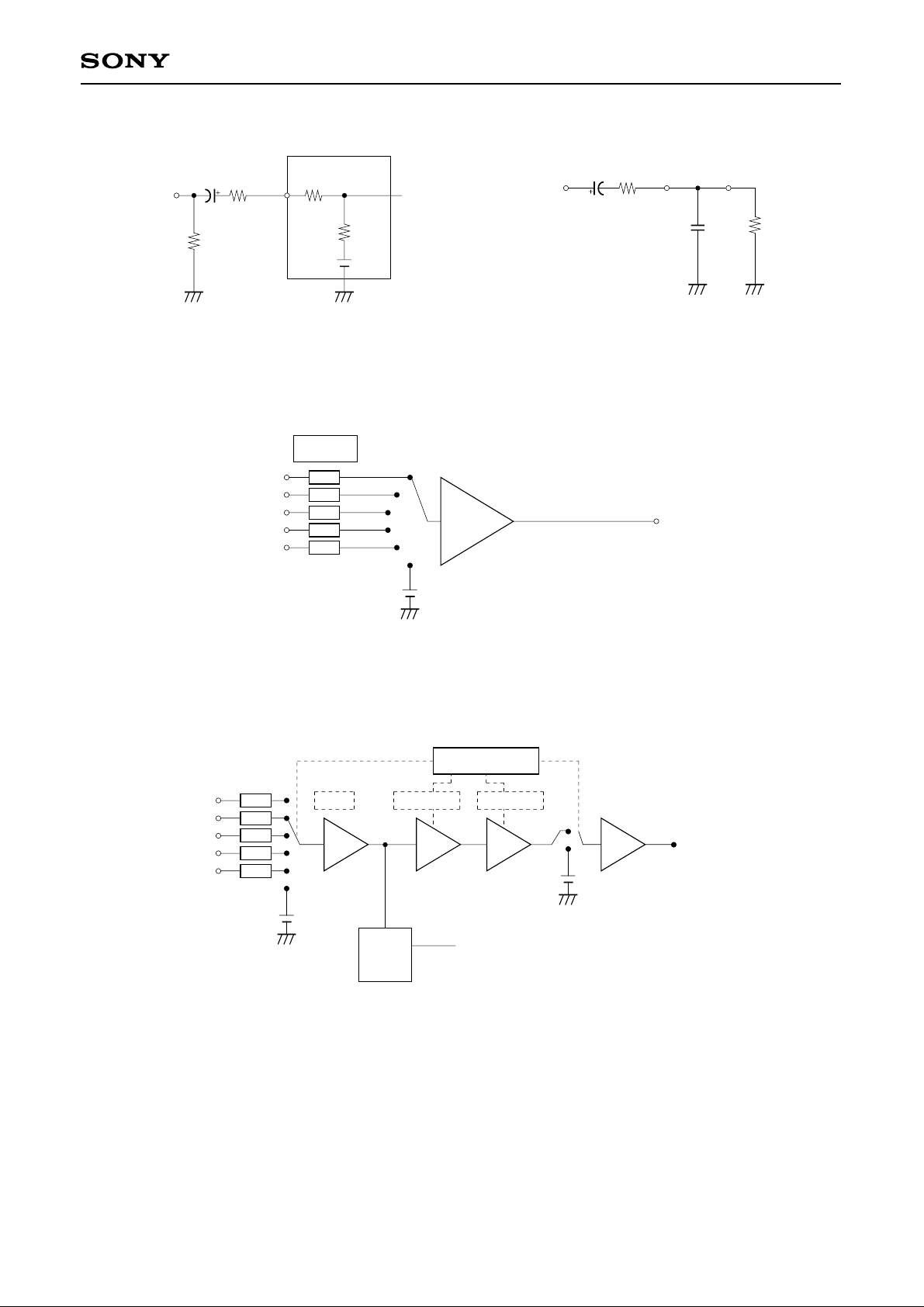
The audio system consists of 5 stereo inputs, 3 stereo outputs and a mono output. Each output can be
independently connected to any one of five inputs, Lin1 to Lin5 for the left stereo audio channel, and Rin1 to
Rin5 for the right hand audio channel. In all cases, the input to the switch and amplifier is composed of a
potential divider consisting of a 27kΩ series resistor and a 33kΩ connected to a voltage source (4.5V). When
used in conjunction with an external 6kΩ series input resistor, the input configuration forms a –6dB attenuator
(Fig. 2-1). The net gain of the audio system is zero as there is an internal +6dB amplifier on each output. The
output impedance of the audio amplifier is near zero, and is used to drive the external SCART circuit. The
output is capacitively coupled through a 10µF capacitor, and an optional 600Ω series compliance resistor.
Depending on the length and type of cable used in the scart cable connector, the load seen at the scart
terminal will consist of a parallel capacitor, (100pF to 400pF) and mandatory 10kΩ resistor connected to
ground (Fig. 2-2). The customer may chose to place an alternative audio output filter at the AV switch output.
TV audio output
The TV audio section is composed of an audio switch and 0dB amplifier followed by two variable gain stages,
corresponding to the course and fine electronic volume control amplifiers, EVC and EVF. The EVC amplifier
attenuates the input signal in steps of 8dB. A range of attenuation from 0dB to 56dB can be programmed by
means of the I2C interface. Similarly, the fine volume control (EVF) can be programmed to provide a range of
attenuations between 0dB and 7dB. The attenuated signal is passed through to the output buffer stage which
provides the necessary +6dB gain, and is used to drive the SCART connector. The final output buffer can also
act as a –80dB (mute) amplifier (Fig. 2-4).
Zero Cross Detector (ZCD)
The zero cross detector reduces the effect of "click noise" when implementing a volume change or an audio
mute. The change volume or mute instruction sent by I2C will only be implemented when a minimal (ie zero
cross) signal amplitude is detected.
The zero cross detection circuit can be turned off by setting the "ZCD" bit low in the I2C write mode.
The status of the zero cross detector can be checked in the I2C read mode (Z.C status). When this bit is high,
a zero cross condition has been detected subsequent to the issue of an I2C volume change or mute
instruction. This may be useful if the input waveform is very low frequency, whereupon the microprocessor can
re-issue the same instruction, with the zero cross detector circuit switched off.
I2C Mute
The mute instruction in the I2C format refers to the TV audio circuit. Audio mute can be implemented after a
audio zero cross detection, or immediately depending on whether ZCD = 1 or 0.
It can be seen from the I2C write format that the same mute bit occurs in DATA1 and DATA5. This allows the
software to action an immediate mute, make any suitable changes to the audio source or electronic volume
control and after a minimum period of 4 × 90µs (360µs) un-mute the output buffer. Such a period provides
ample time to allow any transient ac voltages to settle during an audio source change.
– 22 –
Page 23
CXA2078Q
Audio in
1µF
R/L in
(external)
600Ω
ATT = –6dB
27kΩ6kΩ
(internal)
Fig. 2-1. Audio input configuration
–6dB
R/L in
R/L in
R/L in
R/L in
R/L in
ATT
ATT
ATT
ATT
ATT
33kΩ
4.5V
Mute
4.5V
+6dB
10µF
Audio out
600
(external)
SCART
400pF
Fig. 2-2. Audio output configuration
Audio
output
Terminal
10kΩ
Fig. 2-3. VCR and AUX audio configuration
I2C Registers
Zero
Cross
Detect
0 to –56dB 0 to –7dB0dB
EVC EVF
to control
logic
+6dB
Mute
(–80dB)
ATT
ATT
ATT
ATT
ATT
Mute
Audio
Switch
Fig. 2-4. T.V. audio section and Electronic Volume Control
TV
Audio
Output
– 23 –
Page 24

I2C Interface Data Format
IC Control Data Format
Slave address A DATA1 A DATA2 A DATA3 A DATA4 A DATA5 A PS
S: Start condition A: Acknowledge P: Stop condition
There are two possible addresses depending on external address pin (12) tied high or low.
Pin 12 = high, Address = 92 Hex Ao = 1
Pin 12 = low, Address = 90 Hex Ao = 0
General I2C data structure (write mode)
CXA2078Q
b2
0
TVMute
Aud_Sw1 (TV)
Aud_Sw2 (VCR)
Aud_Sw3 (AUX)
b1
Ao
LOG2LOG3 LOG1
Address
Data1
Data2
Data3
Data4
Data5
b7
1
Y/C Mix
TVMute
FBLK
FNC
b6
0
EVC
x
x
b5
0
Vid_Sw1 (TV)
Vid_Sw2 (VCR)
Vid_Sw3 (AUX)
b4
1
x LOG4x
b3
0
EVF
Key
EVC: Electronic Volume Course (8dB steps)
EVF: Electronic Volume Fine (1dB steps)
TVMute: TV Audio mute. Controls the TV audio output buffer. (Same bit appears in data 1 & 5)
Z.C.D: Zero cross detector active. When ZCD = 1 volume and mute change at zero cross.
Vid_Sw1: Selects the input video sources for Vout1, Vout2, Vout3, Vout4
Vid_Sw2: Selects the input video sources for Vout5, Vout6
Vid_Sw3: Selects the input video sources for Vout7
Aud_Sw1: Selects one of 5 stereo inputs for RTV, LTV
Aud_Sw2: Selects one of 5 stereo inputs for Rout1, Lout1
Aud_Sw3: Selects one of 5 stereo inputs for Rout2, Lout2
FNC: Video function switch control
FBLK: Video Fast Blanking control
Y/C Mix: When Y/C Mix = 1 converts Y/C input to CVBS for output through Vout8
LOG1-LOG4: Logic outputs (open collector). 0 = high impedance. 1 = current sink mode.
b0
(W) 0
Z.C.D
– 24 –
Page 25
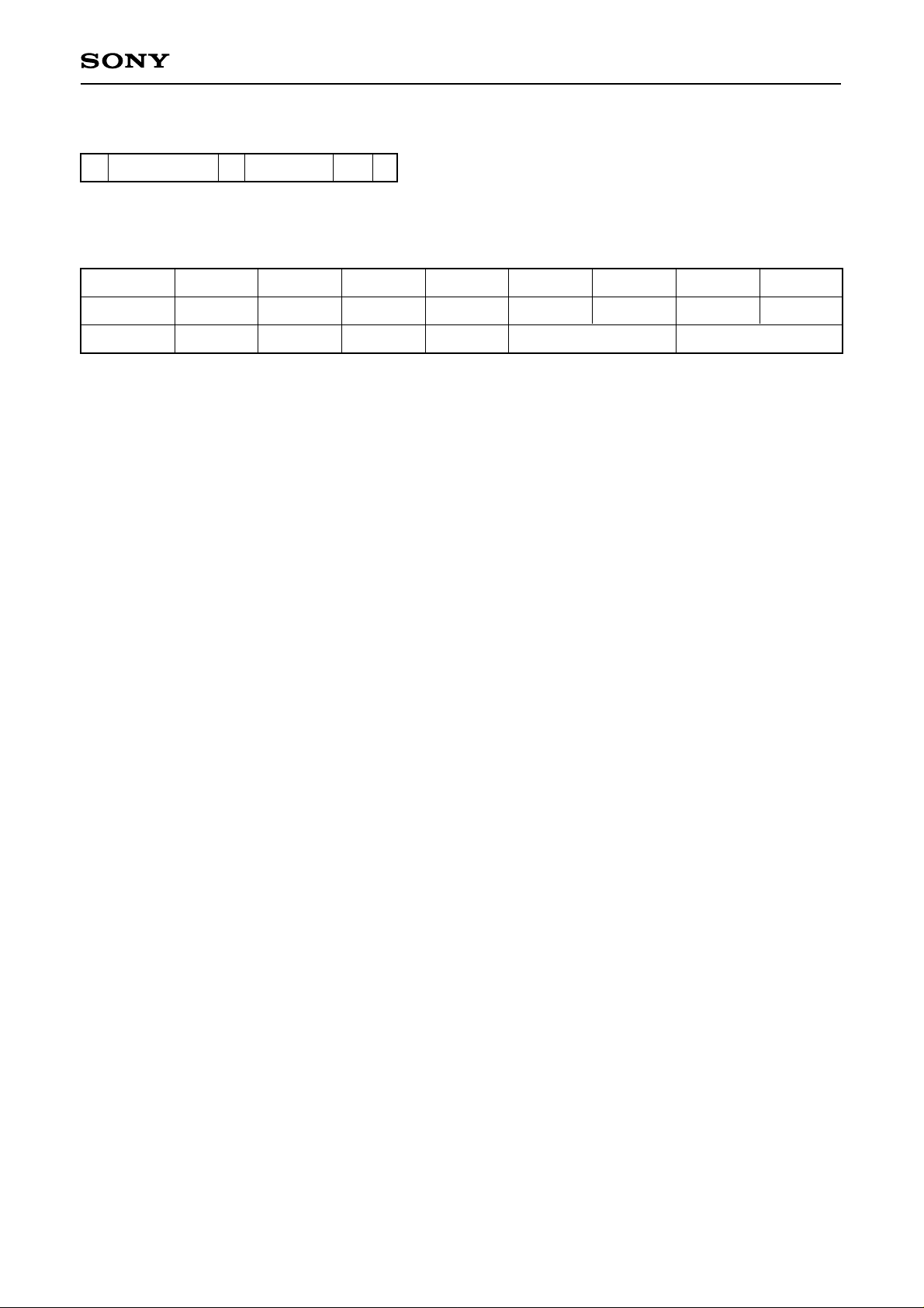
General I2C data structure (read mode)
Slave address A DATA6 PNAS
NA: No Acknowledge
DATA STRUCTURE
CXA2078Q
b1
X
FUNC_VCR
b0
(R) 1
Slave Address
Data6
b7
b6
1
x
0
x
b5
0
ZC
STATUS
b4
1
b3
0
P.O.D. FUNC_AUX
b2
0
FUNC_VCR: At pin 5 AV switch monitors the voltage of pin 8 from VCR scart, and records status.
FUNC_AUX: At pin 7 AV switch monitors the voltage of pin 8 from AUX scart, and records status.
ZC Status: ZC Status = 1 indicates that zero cross condition has been achieved after a volume or mute
instruction issued.
P.O.D.: Power On Detect. P.O.D. = 1 when DIG_VCC voltage rises above a threshold level of
approximately 5V.
– 25 –
Page 26

3. Video Input I2C Control
3-1. Video Switch 1 (Vid_Sw1) – TV Output
Vout1 Vout2 Vout3 Vout4 Comment
B G/CVBS/Y R/C CVBS/Y
d2_b5 d2_b4 d2_b3
CXA2078Q
0
0
0
0
1
1
1
1
0
0
1
1
0
0
1
1
0
1
0
1
0
1
0
1
Vin1
Vbias
Vbias
Vin2
Vbias
Vin1
Vin1
Vbias
Vin3
Vbias
Vbias
Vin4
Vbias
Vin3
Vin3
Vbias
Table 3-1. showing which video input pins connect to the four TV output pins
3-2. Video Switch 2 (Vid_Sw2) – VCR Output
Vout5 Vout6 Comment
Chroma (C) CVBS/Y
d3_b5 d3_b4 d3_b3
0
0
0
0
0
1
0
1
0
Vin5
Vin6
Vin7
Vin9
Vin10
Vin11
Vin5
Vin6
Vin7
Vin8
Vin5
Vin5
Vin5
Vbias
Digital encoder
Digital encoder
VCR
Vin9
Vin10
Vin11
Vin12
Vin3
Vin10
Vin11
Vbias
Digital encoder
Digital encoder
VCR
Aux
Digital encoder
Digital encoder
Digital encoder
Video Mute
0
1
1
1
1
1
0
0
1
1
1
0
1
0
1
Vin8
Vin5
Vbias
Vbias
Vbias
Vin12
Vin3
Vbias
Vbias
Vbias
Aux
Digital encoder
Video Mute
Video Mute
Video Mute
Table 3-2. showing which video input pins connect to the two VCR output pins
– 26 –
Page 27
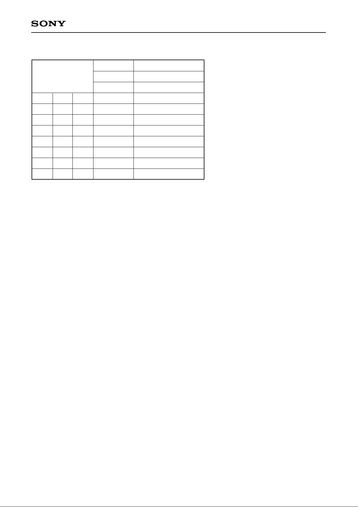
3-3. Video Switch 3 (Vid_Sw3) – AUX Output
Vout7 Comment
CVBS
d4_b5 d4_b4 d4_b3
CXA2078Q
0
0
0
0
1
1
1
1
0
0
1
1
0
0
1
1
0
1
0
1
0
1
0
1
Vin9
Vbias
Vin11
Vin12
Vin3
Vbias
Vbias
Vbias
Digital encoder
Video Mute
VCR
Aux
Digital encoder
Video Mute
Video Mute
Video Mute
Table 3-3. showing which video input pins connect to the single AUX output pin
– 27 –
Page 28

CXA2078Q
4. Fast Blanking operation (Pin 16 on SCART), FBLK
The fast blanking signal instructs the TV to select either the external CVBS information or the external RGB
information. This is used to impose an on screen display (OSD) presentation (normally RGB) upon a CVBS
background. Fast blanking information has the same nominal phase as the RGB and CVBS signal, and is
defined as follows,
Fast blanking output at scart,
1. CVBS mode Scart pin voltage = 0 to 0.4V
2. RGB mode Scart pin voltage = 1 to 3.0V
Threshold voltage is approximately 0.75V DC voltage at scart input.
The blanking information is usually generated by the same source as that producing the RGB signal.
I2C Control
In the CXA2078Q, there are two fast blanking inputs, one associated with the auxiliary RGB/CVBS inputs and
another associated with Digital Encoder input. These can be selected by I2C. In addition to the two blanking
inputs, the fast blank pin output can be set to a constant 0V or 5V by means of the I2C control. Hence there are
four possible states. These are controlled according to the following table.
FBLK
d2_b7
d2_b6
0
0
1
1
∗1
Default = 0V at power up
FBLK_OUT (pin 53)
0V
0
5V
1
same state as FBLK_IN1 (0/5V)
0
same state as FBLK_IN2 (0/5V)
1
∗1
– 28 –
Page 29
CXA2078Q
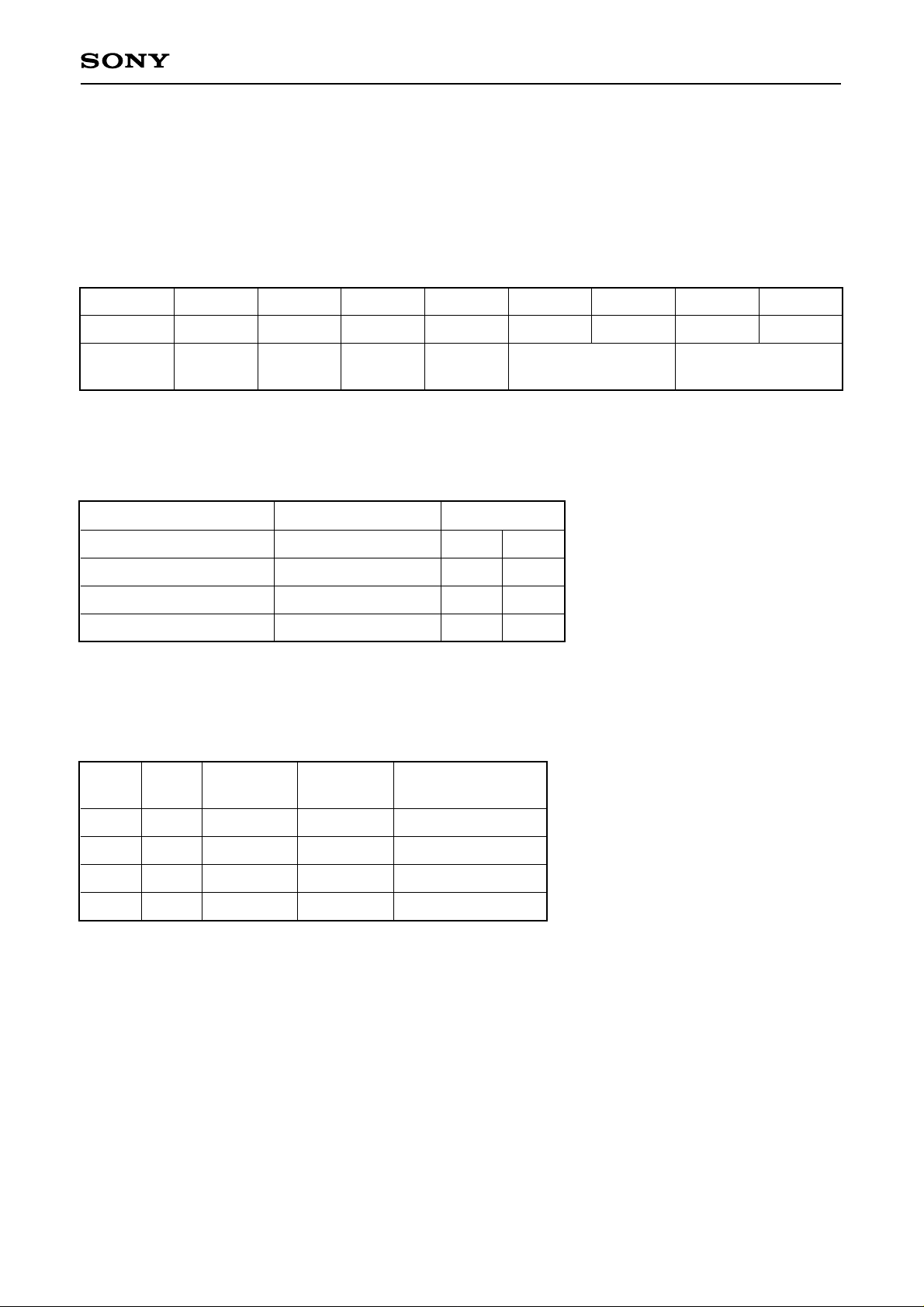
5. Function switch, FNC.
The function switch facility is designed to read the status of the SCART function pin 8 from the VCR and AUX
inputs (IC pin 5, 7). The output function pins FNC_TVA and FNC_TVB are controlled from the IC using a write
instruction. A suitable interface circuit (fig 5-2) will allow FNC_TVA and FNC_TVB to instruct the TV to switch
between display modes.
Read Mode DATA STRUCTURE
b1
Slave Address
Data6
b7
b6
1
0
b5
0
Z.C
STATUS
b4
1
b3
0
P.O.D. FUNC_AUX
b2
0
Read mode
Status of I2C registers as a function of the voltage on FNC_AUX (pin 7) and FNC_VCR (pin 5)
read data6Input Pin Voltage
FNC_AUX or FNC_VCR
0V to +2V (default)
+4.5 to +7V
+9.5 to +12V
Level (SCART Defn)
(Internal TV)
(16:9 External)
(4:3 External)
b3/b1
b2/b0
0
0
1
0
1
1
Write mode TV Function switch, Interface table
X
FUNC_VCR
b0
(R) 1
d3_b7
0
0
1
1
d3_b6
0
1
0
1
FNC_TVA
Pin voltage
2V
0V
0V
0V
FNC_TVB
Pin voltage
2V
2V
0V
0V
Default is Internal TV (0, 0) at power up
Comment
Internal TV (default)
External 16:9
External 4:3
External 4:3
– 29 –
Page 30
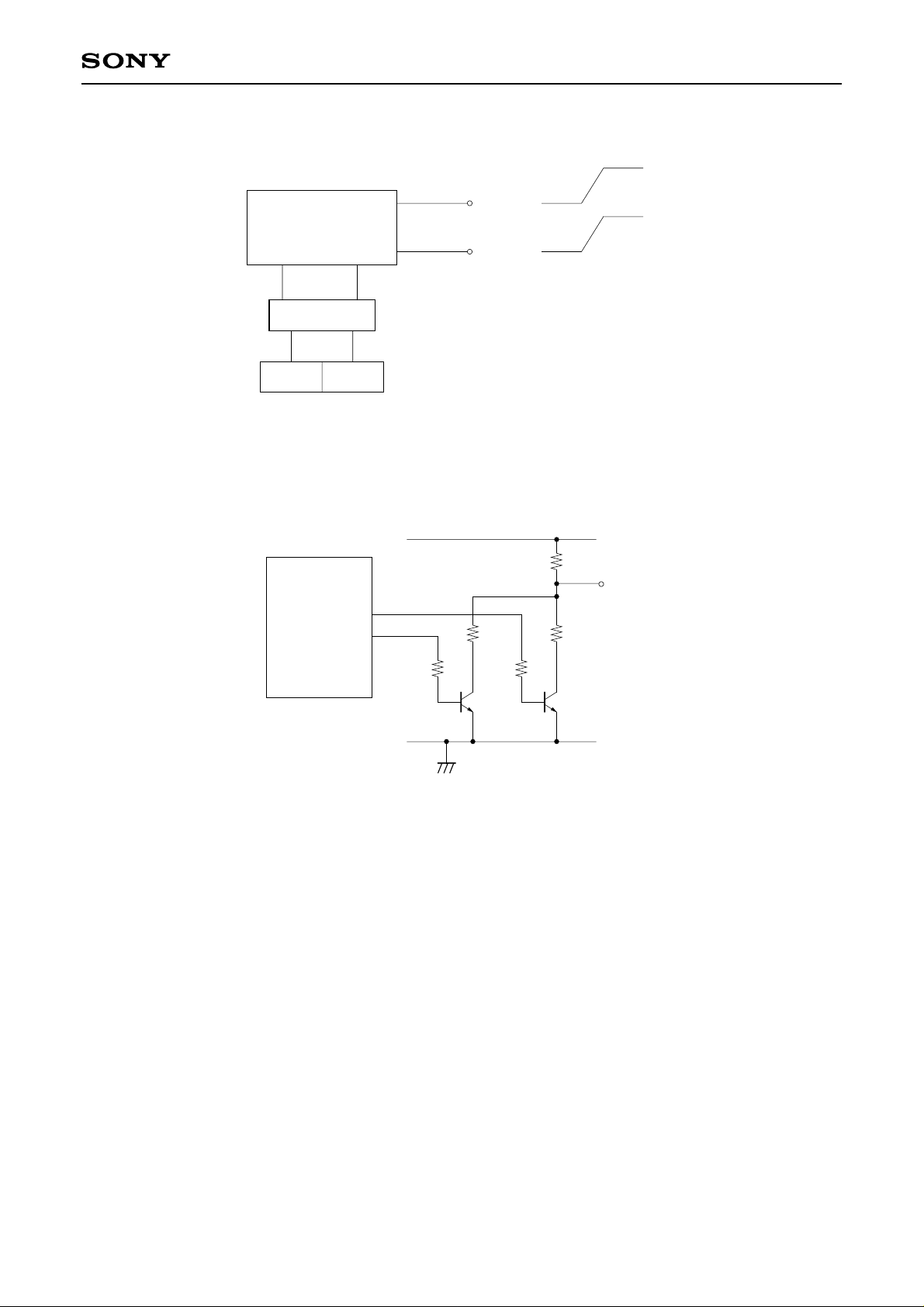
The two function output pins are controlled via logic to swing from 0 to +2V.
CXA2078Q
2V
FNC_TVA (38)
Logic Drive
Circuit
FNC_TVB (37)
Mux
d3_b7 d3_b6
< 0.4V
2V
< 0.4V
Fig. 5-1. TV Function switch output
Some external circuitry is required to interface from the IC pins to the SCART pin 8. A typical interface circuit is
shown in Fig. 5-2.
12V
1kΩ
TV scart
FNC_TVA
FNC_TVB
1kΩ
pin 8
50Ω
2.2kΩ
CXA2078Q
2.2kΩ
Fig. 5-2. External circuit for function switch
– 30 –
Page 31
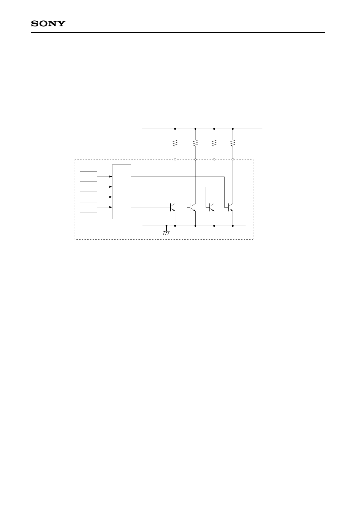
6. Logic outputs
I2C control of logic outputs achieved using bits LOG1 – 4.
Specification
I2C bit 0 = open collector/high output impedance on logic pin
I2C bit 1 = current sink mode resulting in 0.2V saturation voltage on logic pin
Vmax at logic pin = 12V
Imax during current sink = 1mA
V
CC = 9V
CXA2078Q
d5_b3
d5_b2
d5_b1
d5_b0
Logic
Logic
cct.
cct.
10kΩ
LOG_1
10kΩ
LOG_2
Fig. 6-1. Open collector logic outputs
10kΩ
LOG_3
10kΩ
LOG_4
External
resistors
– 31 –
Page 32
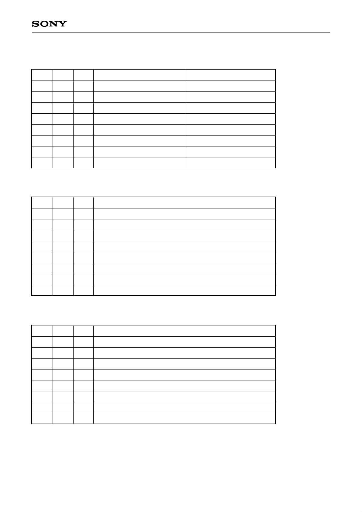
7. I2C Audio Signal Control
I2C Audio input select using Aud_Sw1 (TV), Aud_Sw2 (VCR), Aud_Sw3 (AUX)
CXA2078Q
b2 b1 b0
0
0
0
0
1
1
1
1
0
0
1
1
0
0
1
1
0
1
0
1
0
1
0
1
RTV, ROUT1, ROUT2 LTV, LOUT1, LOUT2
Rin1
Rin2
Rin3
Rin4
Rin5
Audio mute
Audio mute
Audio mute
I2C Electronic Volume control (coarse) DATA 1, EVC
b7 b6 b5
0
0
0
0
0
0
1
1
0
1
0
1
Gain (dB)
–16
–24
Lin1
Lin2
Lin3
Lin4
Lin5
Audio mute
Audio mute
Audio mute
0
–8
1
1
1
1
0
0
1
1
0
1
0
1
I2C Electronic Volume control (fine) DATA 1, EVF
b4 b3 b2
0
0
0
0
1
1
1
1
0
0
1
1
0
0
1
1
0
1
0
1
0
1
0
1
–32
–40
–48
–56
Gain (dB)
0
–1
–2
–3
–4
–5
–6
–7
– 32 –
Page 33
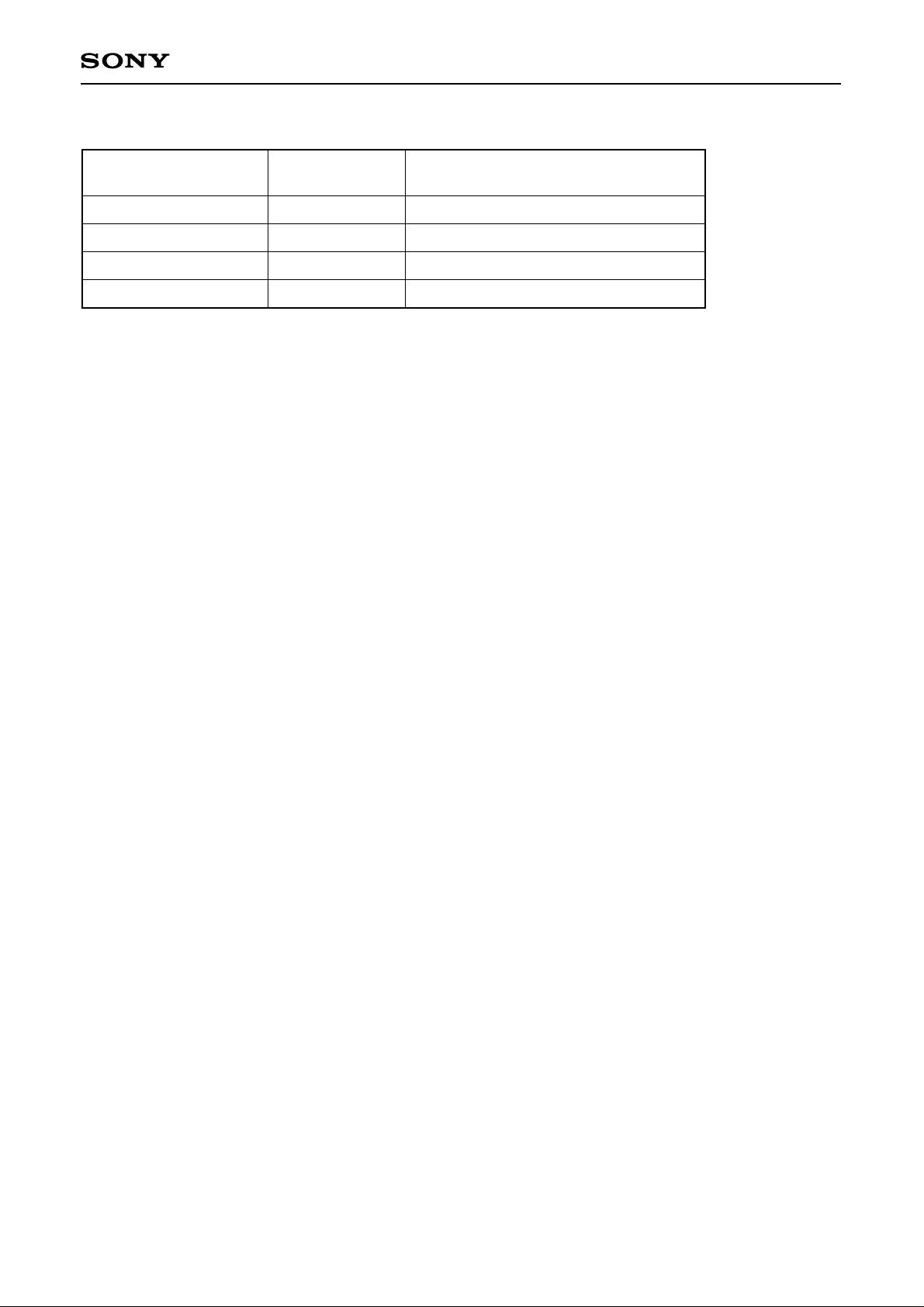
I2C Mute function
CXA2078Q
TV Mute
DATA1 b1 DATA5 b7
0
0
1
1
Z.C.D
DATA1 b0
0
1
0
1
RTV, LTV, MONO output
Un-mute immediately
Un-mute on next zero cross
Mute immediately
Mute on the next zero cross
Notes on operation
1) Supply de-coupling capacitors, 10nF and 4.7µF in parallel should be inserted as close to the supply pins,
25, 47, 58 as possible.
2) To minimise crosstalk, attention should be given to the routing of audio and video to the IC inputs. PCB
track lengths should be kept as short as possible and preferably, audio placed on a separate layer to the
video.
3) The trap components on pin 35 should be kept as close to the IC as possible to minimise parasitic
capacitance to ground.
4) Attention should be given to the electrolytic capacitors on the input and output signal pins. As the pin's
voltage is between 3.7V and 4.7V dc the positive terminal on the capacitor should be orientated towards the
pin.
5) The audio outputs may be muted at any time after power up by connecting the HW MUTE pin (40) to a
voltage > 2.5V and < 9V.
6) The I2C address of the IC can be changed using the ADR pin (12). By connecting this pin to >5V and <9V
the Address changes from 90H to 92H.
7) When driving video loads with impedance = 75Ω an emitter follower or video line driver is required to be
connected at the video outputs.
Stray capacitance on pins Vout1-8 must be kept to a minimum by placing loads as close to the pins as
possible.
8) As shown on the application schematic, static protection for pins 38 and 37 may typically be achieved using
Zener diodes. Diodes with a Zener voltage > 5V are suitable.
– 33 –
Page 34

Typical audio output distortion
Input = 1kHz,
400Hz – 80kHz BPF
1
0.1
THD [%]
0.01
0.001
0 1 2 3 3.66
Input [Vrms]
Audio frequency characteristics
CXA2078Q
4
2
0
–2
Audio input/output gain [dB]
–4
–6
100 1k 10k 100k 1M
NOTE: Audio input 6kΩ resistor removed for this test.
Input = 0.3Vp-p
Frequency [Hz]
Video frequency characteristics
8
6
4
VOUT1-8 (MIX = OFF)
2
Video input/output gain [dB]
0
100k
VOUT8 (MIX = ON)
Input = 0.3Vp-p
1M 10M 50M
Frequency [Hz]
– 34 –
Page 35
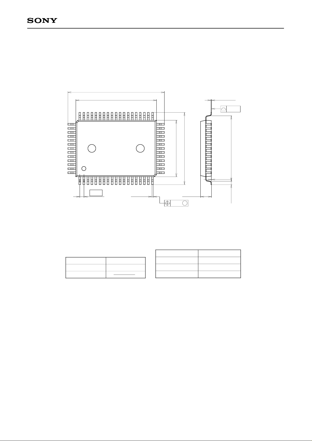
Package Outline Unit: mm
CXA2078Q
64PIN QFP(PLASTIC)
23.9 ± 0.4
+ 0.4
20.0 – 0.1
51
52
64
1
1.0
0.4 – 0.1
+ 0.15
33
32
+ 0.4
14.0 – 0.1
17.9 ± 0.4
20
19
± 0.12
+ 0.35
2.75 – 0.15
M
+ 0.1
0.15 – 0.05
+ 0.2
0.1 – 0.05
0.15
16.3
0.8 ± 0.2
SONY CODE
EIAJ CODE
JEDEC CODE
QFP–64P–L01
QFP064–P–1420
PACKAGE STRUCTURE
PACKAGE MATERIAL
LEAD TREATMENT
LEAD MATERIAL
PACKAGE MASS
EPOXY RESIN
SOLDER/PALLADIUM
42/COPPER ALLOY
1.5g
PLATING
– 35 –
 Loading...