

Page 1
CXA2108Q
Constant-Current Driver for Full Color LED Display
Description
The CXA2108Q is a 1,024-gradation LED driver
which is ideal for full color LED displays. This IC has
24 outputs and a maximum output current of 60mA.
Time division allows driving of either two or six LEDs
per output by connecting an external FET or other
switch. The luminance (PWM) and drive current for
each LED are set using the internal RAM. The LED
type is common anode.
Features
• 24 outputs: 10-bit (1,024-gradation) PWM current outputs
• Maximum output current: 60mA
• LED type: Common anode
• 4-bit brightness function capable of switching the basic PWM pulse width in 16 steps
• Time division allows driving of up to six LEDs with a single output, making it possible to configure a high
definition display with few driver ICs.
• Coarse Adj. (2 bits) and Fine Adj. (8 bits) output current adjustment for each LED makes it possible to drive
R, G and B using the same output from the same IC. In addition, the characteristics variance of each LED
can also be corrected.
• All luminance (PWM) data and drive current data are set by writing to the internal RAM.
• PWM emitting can be performed up to 15 times per frame to realize a screen with little flicker.
• Two built-in PWM data RAM make it possible to set the next luminance data even during PWM operation.
• Abnormal internal temperature detection circuit
• Single 5V power supply
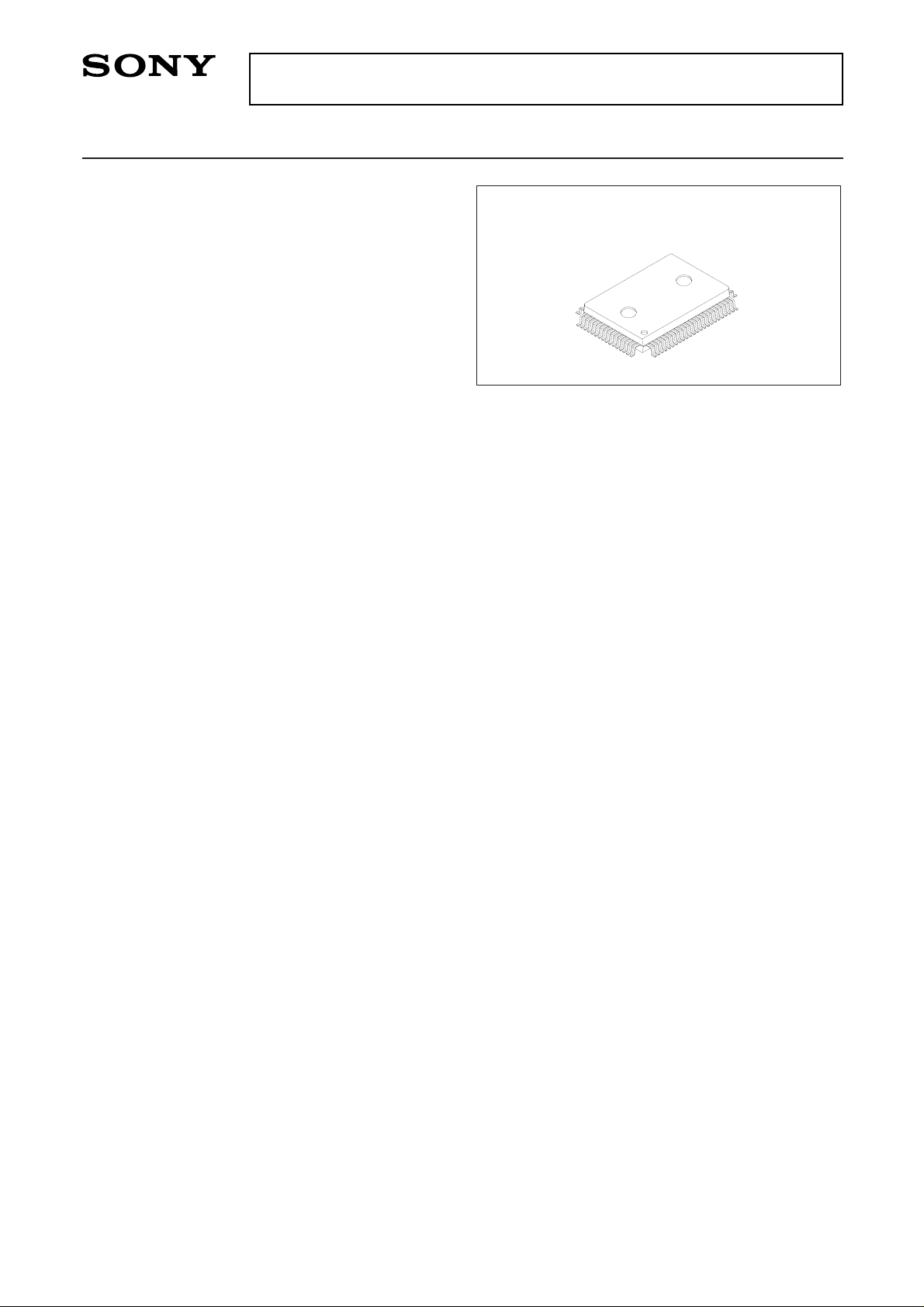
• Surface mounting package (80-pin QFP)
Applications
LED display panels
Structure
Bi-CMOS silicon monolithic IC
Absolute Maximum Ratings (Ta = 25°C)
• Supply voltage AVCC, DVCC –0.3 to +6.0 V
• Digital input voltage VI_D –0.3 to DVCC + 0.3 V
• Digital output current Io_D –5.0 to +5.0 mA
• Driver output voltage V_DVR 0 to AVCC + 0.3 V
• Driver output current I_DVR –1 to +80 mA
• Operating temperature
∗1
Topr –40 to +80 °C
• Storage temperature Tstg –65 to +150 °C
• Allowable power dissipation∗1(Ta = 65°C or less) PD 1.5 W
Recommended Operating Range
• Supply voltage AVCC, DVCC 4.75 to 5.25 V
• Driver output compliance voltage Vcmp 1.5 to AVCC + 0.3 V
• Operating temperature (ambient temperature)
∗1
Ta –20 to +65 °C
• Operating temperature (case temperature)
∗1
Tc –20 to +110 °C
∗1
When mounted on a printed circuit board
– 1 –
E98333B91-PS
Sony reserves the right to change products and specifications without prior notice. This information does not convey any license by
any implication or otherwise under any patents or other right. Application circuits shown, if any, are typical examples illustrating the
operation of the devices. Sony cannot assume responsibility for any problems arising out of the use of these circuits.
80 pin QFP (Plastic)
For the availability of this product, please contact the sales office.
Page 2
– 2 –
CXA2108Q
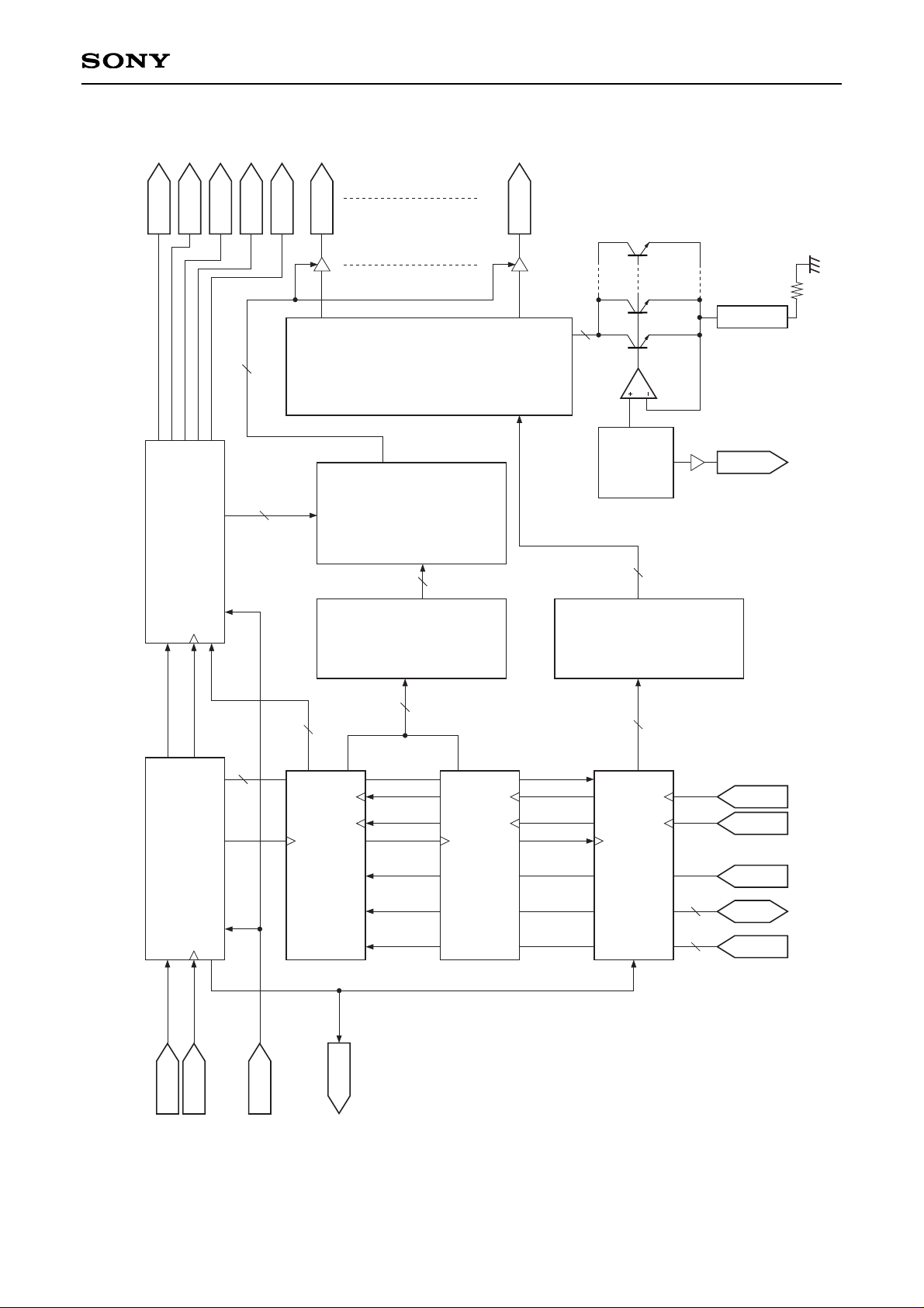
Block Diagram
PWM data RAM (B)
(6word × 24ch × 10bit)
PWM data RAM (A)
(6word × 24ch × 10bit)
Data Read Counter
Drive Current data RAM
(6word × 24ch × 10bit)
10bit × 24
Shift Reg.
&
Latch
PWM data
10bit × 24
Shift Reg.
&
Latch
8bit DAC with
2bit coarse Adj.
(× 24)
× 24
DLDI
CLK
IOUT23
A0 to 9
10
MODE
RDY
D0 to 9
XTAO
REXT
XR/W
XRD
XWR
10
10
DATA
10 × 24
Rext
24
10 × 24
24
PWMout
PWM Counter
10
DATA
4
10
Counter
out
Data
Comparator
Band
Gap
Ref.
9
BRT
R_ADRR_CLK
IOUT0
XB
XG
XR
XUPR
DLDO
Drive
Current
data
Page 3
– 3 –
CXA2108Q
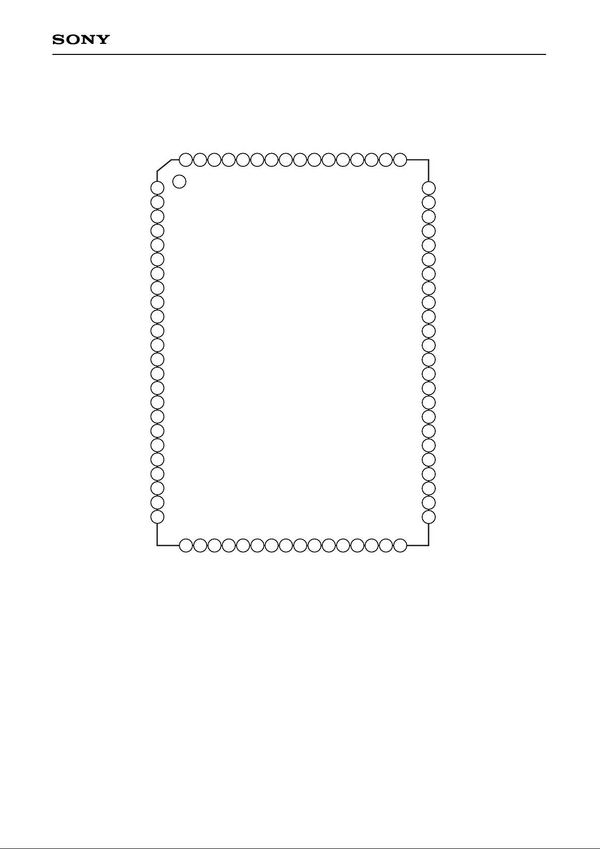
Pin Configuration (Top View)
25 26 27 28 29 30 31 32 33 34 35 36 37 38 39
40
45
46
47
48
49
50
51
52
53
54
55
56
57
58
59
60
61
62
63
64
65666768697071727374757677787980
1
2
3
4
5
6
7
8
9
10
11
12
13
14
15
16
17
18
19
20
D1
D2
D3
D4
D5
D6
D7
D8
D9
A0
A1
A2
A3
A4
A5
A6
IOUT5
IOUT4
IOUT3
IOUT2
IGND
IOUT1
IOUT0
AV
CC
AGND
REXT
NC
NC
XTAO
XRST
XR/W
XRD
XWR
XCS
DLDI
A9
41
42
43
44
A8
DV
CC
DGND
A7
IOUT18
IOUT19
IOUT20
IOUT21
IGND
IOUT22
IOUT23
AV
CC
AGND
NC
MODE
DGND
RDY
DLDO
21
22
23
24
CLK
DGND
DV
CC
D0
WALL
XUPR
TEST_O
XB
XR
XG
IOUT17
IGND
IOUT16
IOUT15
IOUT14
IGND
IOUT13
IOUT12
IOUT11
IOUT10
IGND
IOUT9
IOUT8
IOUT7
IGND
IOUT6
Page 4
– 4 –
CXA2108Q
Pin
No.
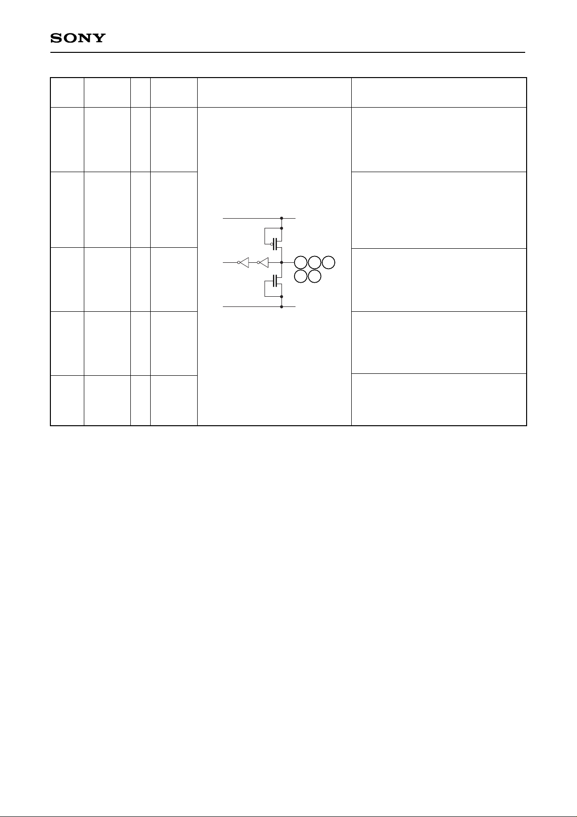
Symbol Equivalent circuit Description
Reference
voltage
level
I/O
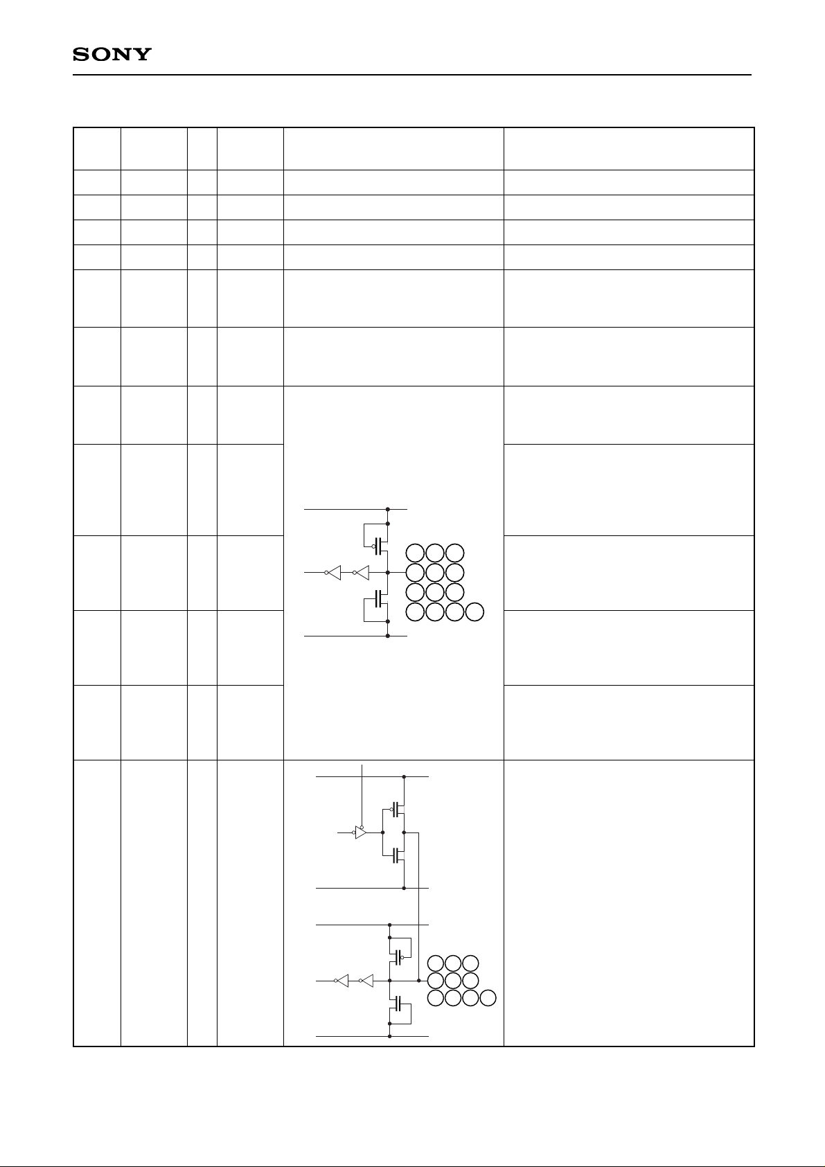
Pin Description
Analog GND.
9, 56
AGND
GND
—
Analog power supply.
8, 57
AVCC
5V (Typ.)
—
Digital GND.
12, 22, 42
DGND
GND
—
Digital power supply.
23, 43
DVCC
5V (Typ.)
—
GND for driver output.
5, 60,
66, 70,
75, 79
IGND
GND
—
Open.
This pin is not connected with the
internal circuits.
10,
53, 54
NC
DGND
DV
CC
40
37
34
21
41
38
35
51
44
39
36
11
45
—
Clock input.
Driver operation is synchronized with
this clock.
Reset input.
The IC is initialized by inputting low
level. However, the memory is not
initialized. Input high level during
normal operation.
Output mode switching.
Upper/Lower mode for low level input.
Upper/Lower/RGB mode for high level
input. (See the Description of Operation.)
Address input.
These pins are used to input the internal
RAM (luminance data, brightness data
and drive current data RAM) address.
RAM selection.
The luminance data RAM is selected
when this pin is low, and the drive
current data RAM when high.
21
CLK
CMOS
I
51
XRST
CMOSI
11
MODE
CMOS
I
34 to 41,
44
A0 to 8
CMOS
I
45
A9
CMOSI
DGND
DV
CC
30
27
24
31
28
25
32
29
26
33
DGND
DV
CC
Data I/O.
These pins are used to input and
output data to and from the internal
RAM (luminance data, brightness data
and drive current data RAM). See
Table 1. Read/Write Switching
Condition Correspondence Table for
the data I/O switching conditions.
24 to 33
D0 to 9
CMOS
I/O
Page 5
– 5 –
CXA2108Q
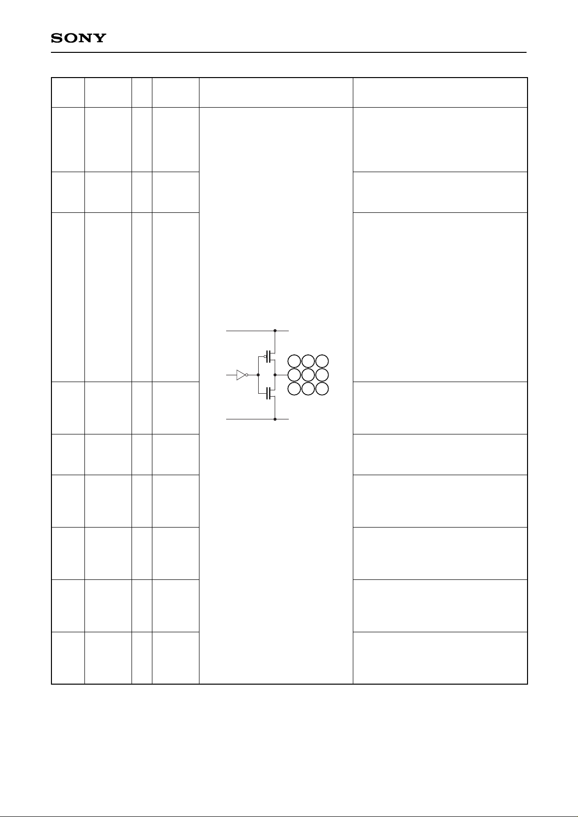
Internal RAM chip select.
Internal RAM access is enabled by
inputting low level. (See Table 1.
Read/Write Switching Condition
Correspondence Table.)
Internal RAM read/write select.
Write mode is selected for high level, and
read mode for low level. See Table 1.
Read/Write Switching Condition
Correspondence Table for the actual
read/write switching signal input conditions.
Write clock input.
This pin is used to input the clock for
writing the luminance, brightness and
drive current data. It is not
synchronized with CLK.
Read clock input.
This pin is used to input the clock for
externally reading the luminance,
brightness and drive current data. It is
not synchronized with CLK.
Trigger signal input for luminance data
RAM (A)/(B) switching and PWM
output start.
(See the Timing Charts.)
47
XCS
CMOS
I
50
XR/W
CMOS
I
48
XWR
CMOS
I
49
XRD
CMOS
I
46
DLDI
CMOS
I
Pin
No.
Symbol Equivalent circuit Description
Reference
voltage
level
I/O
CC
DV
47 48
494650
DGND
Page 6
– 6 –
CXA2108Q
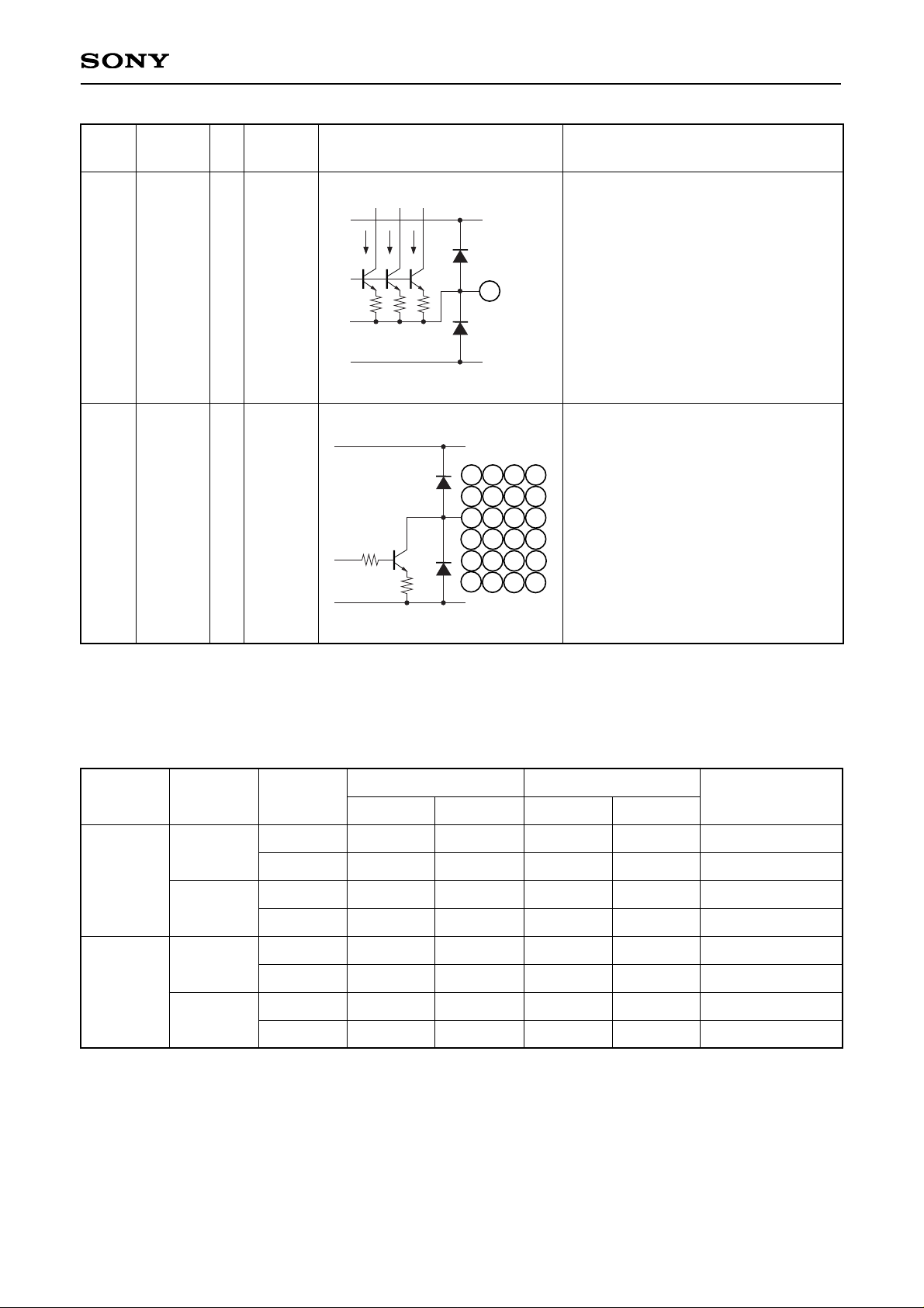
READY signal output.
This indicates the drive current data
RAM access enabled period. Access
is enabled while high level is output.
(See the Timing Charts.)
DLDI signal output.
This outputs the DLDI signal
synchronized with CLK.
Write ALL signal output.
One pulse (= high level signal with a
width of 1 clock) is output
synchronized with the rising edge of
the next CLK after the final address
∗1
of the currently selected mode is input.
Note that both the final address must
be input and the XCS and XWR input
levels must be low at the rising edge
of this CLK.
(See the Timing Charts for details.)
∗1
02Fh (Upper/Lower mode)
08Fh (Upper/Lower/RGB mode)
Upper signal output.
This is used as the LED switching signal.
(See the Timing Charts and Application
Circuits for details.)
Test signal output.
This pin is unrelated to the functions of this IC.
Do not connect anything; leave this pin open.
Blue signal output.
This is used as the LED switching signal.
(See the Timing Charts and Application
Circuits for details.)
Red signal output.
This is used as the LED switching signal.
(See the Timing Charts and Application
Circuits for details.)
Green signal output.
This is used as the LED switching signal.
(See the Timing Charts and Application
Circuits for details.)
Thermal Alarm Out signal output.
This pin normally outputs high level, but it
outputs low level when the internal
temperature rises to an abnormally high level.
13
RDY
CMOS
O
14 DLDO CMOSO
15
WALL
CMOS
O
16
XUPR CMOS
O
17 TEST_O
CMOS
O
18
XB CMOSO
19
XR
CMOS
O
20 XG
CMOS
O
52 XTAO
CMOS
O
Pin
No.
Symbol Equivalent circuit Description
Reference
voltage
level
I/O
13
16
19
DV
14
17
20
CC
15
18
52
DGND
Page 7
– 7 –
CXA2108Q
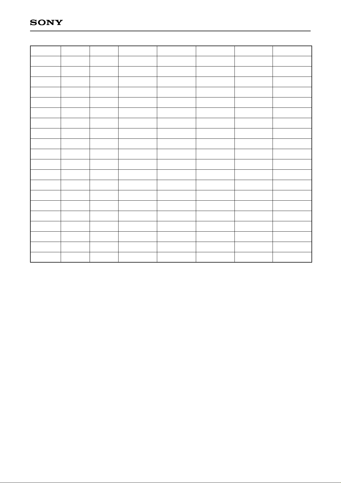
Drivers.
These pins drive the LED.
1 to 4,
6, 7,
58, 59,
61 to 65,
67 to 69,
71 to 74,
76 to 78,
80
IOUT0
to 23
O
XCS
[ I ]
L
H
XR/W
[ I ]
L
H
L
H
A9
[ I ]
L
H
L
H
L
H
L
H
Luminance
Write
Disable
Disable
Enable
Disable
Disable
Disable
Disable
Disable
Enable
Disable
Disable
Disable
Disable
Disable
Disable
Disable
Disable
Disable
Disable
Enable
Disable
Disable
Disable
Disable
Disable
Enable
Disable
Disable
Disable
Disable
Disable
Disable
Read
Drive current
D0 to 9
[I/O]
Output
Output
Input
Input
Hi-Z
Hi-Z
Hi-Z
Hi-Z
Write Read
Table 1. Read/Write Switching Condition Correspondence Table
AGND
AV
CC
55
Drive current setting.
Connect a resistor between this pin
and GND. The drive current is
proportional to the current flowing to
this resistor. (See Table 2. Drive
Current Setting and Power
Consumption.)
55
REXT
O
Pin
No.
Symbol Equivalent circuit Description
Reference
voltage
level
I/O
CC
AV
1 2 3 4
6 7 58 59
61 62 63 64
67 68 69
65
71 72 73 74
76
77
IGND
78 80
Page 8
– 8 –
CXA2108Q
Rext [kΩ]
2.0
2.0
2.0
2.0
2.5
2.5
2.5
2.5
3.0
3.0
3.0
3.0
3.5
3.5
3.5
3.5
4.0
4.0
4.0
4.0
D9
0
0
1
1
0
0
1
1
0
0
1
1
0
0
1
1
0
0
1
1
D8
0
1
0
1
0
1
0
1
0
1
0
1
0
1
0
1
0
1
0
1
Io (FFh) [mA]
21.7
43.3
65.0
∗1
86.7
∗2
17.3
34.7
52.0
69.3
∗1
14.4
28.9
43.3
57.8
12.4
24.8
37.1
49.5
10.8
21.7
32.5
43.3
Io (00h) [mA]
10.8
21.7
32.5
43.3
8.7
17.3
26.0
34.7
7.2
14.4
21.7
28.9
6.2
12.4
18.6
24.8
5.4
10.8
16.3
21.7
Istb [mA]
27.3
48.3
69.2
90.2
22.4
39.2
55.9
72.7
19.1
33.1
47.1
61.1
16.8
28.8
40.8
52.8
15.1
25.6
36.0
46.5
Pstb [W]
0.136
0.241
0.346
0.451
0.112
0.196
0.280
0.364
0.096
0.166
0.235
0.305
0.084
0.144
0.204
0.264
0.075
0.128
0.180
0.233
Po (max) [W]
1.36
1.26
1.15
1.05
1.39
1.30
1.22
1.14
1.40
1.33
1.26
1.19
1.42
1.36
1.30
1.24
1.42
1.37
1.32
1.27
∗1
Operation guaranteed current exceeded.
∗2
Absolute maximum rating exceeded.
Table 2. Drive Current Setting and Power Consumption (when D0 to D7 = FFh)
Rext : External resistor that sets the DAC reference current (Iref)
D9, D8 : Data that sets the maximum drive current (Io (FFh))
Iref : DAC reference current
Iref [mA] = 1.3 [V]/Rext [kΩ]/24
Io (FFh) : Maximum drive current that can be set by D0 to D7
Io (FFh) [mA] = Iref × (2 × D9 + D8 + 1) × 800
Io (00h) : Minimum drive current that can be set by D0 to D7
Io (00h) [mA] = Io(FFh)/2
Istb : Standby current (Internal current consumption excluding the driver block)
Istb [mA] = 2.86 + 24 × Iref × (16/3 + 32.25 × (2 × D9 + D8 + 1))
Pstb : Standby power (Internal power consumption excluding the driver block, Vcc = 5 V)
Pstb [W] = 5 [V] × Istb [mA]/1000
Po (max)
: Maximum power that can be consumed by the driver block
Po (max) [W] = 1.5 [W] – Pstb [W]
Note) Istb, Pstb and Po (max) are the values when D0 to D7 = 11111111 (FFh).
In addition, these values assume the case where all channels are set to the same drive current.
Page 9
– 9 –
CXA2108Q
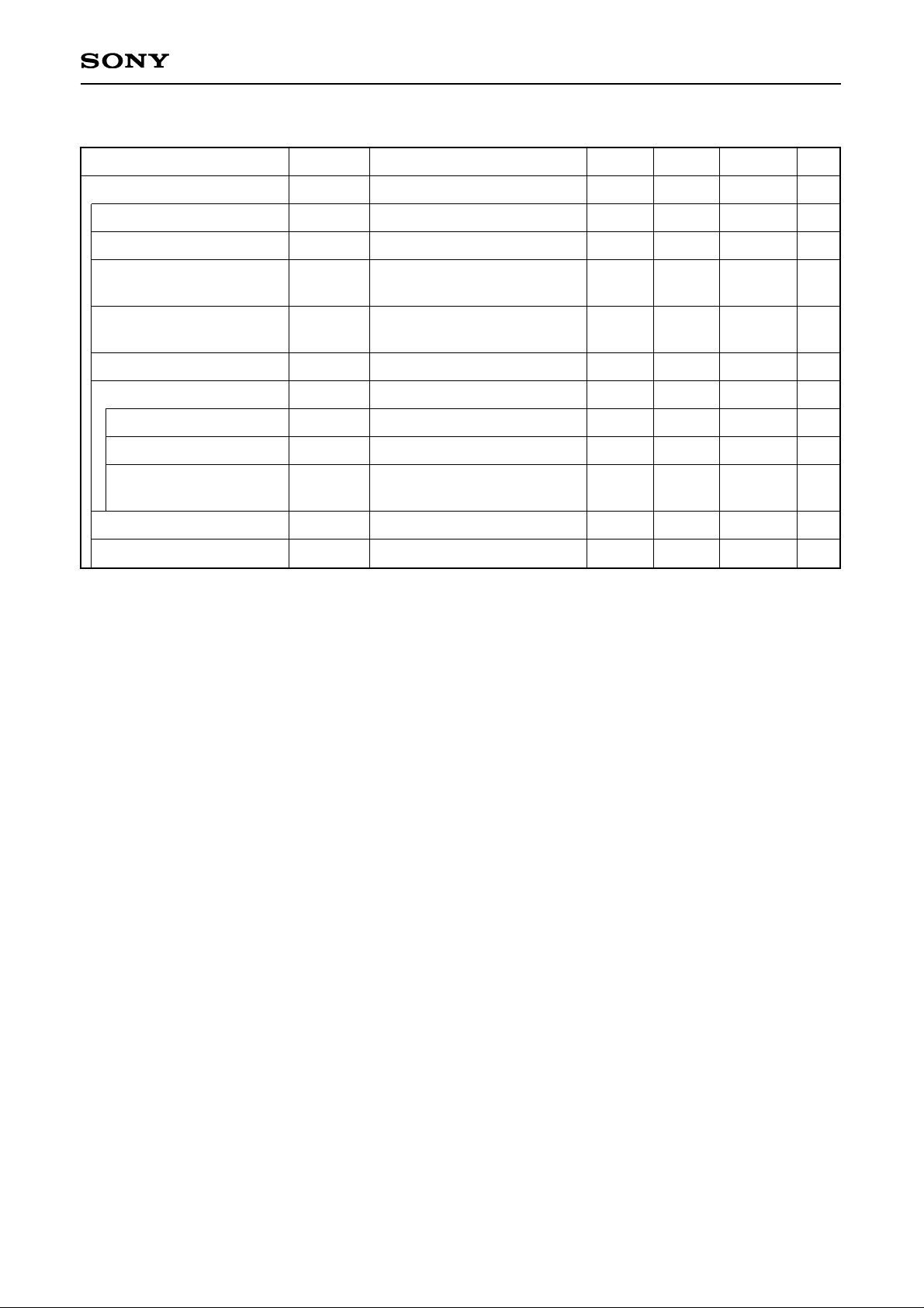
Electrical Characteristics (AVCC, DVCC = +5V, AGND, DGND, IGND = 0V)
PWM output resolution
bit
10
Drive current setting resolution
Coarse Adj.
bit
2
Fine Adj.
bit
8
DLE
±0.8
I
o (FFh) = 60mA
(D0 [LSB] to D7 [MSB] = FFh)
DC characteristics
Differential linearity error
LSB
fCLK
15
PWM reference clock frequency
MHz
Item Symbol Conditions
Min. Typ. Max. Unit
Driver block
VREXT
1356
1253
Rext = 2kΩ
REXT pin voltage
mV
1300
∆VREXT
20
0
VREXT (@AVCC = 5.25V)
– VREXT (@AVCC = 4.75V)
REXT pin voltage
Supply voltage dependency
mV
IDD
35
25
Rext = 2kΩ, D8 = D9 = 0
Note) Excluding the driver block
Standby supply current
mA
IOUT
60
Output current
mA
Vcmp
AVCC + 0.3
1.5
Output compliance voltage
V
Page 10
– 10 –
CXA2108Q
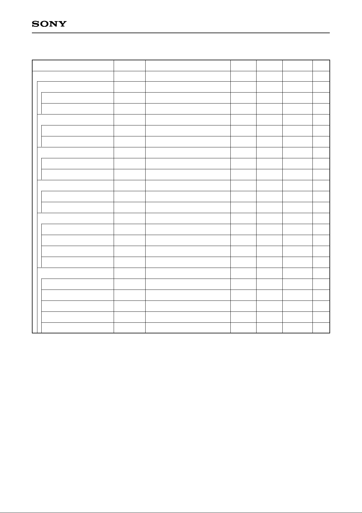
Logic block
Digital input current (I, I/O)
(H)
IIH, IIZH
5
–5
VIN = 5V
µA
(L)
IIL, IIZL
5
–5
VIN = 0V
µA
Digital input voltage (I, I/O)
(H)
VIH, VIZH
DVCC + 0.3
0.7DVCC
VIN = 5V
V
(L)
VIL, VIZL
0.3DVCC
–0.3
VIN = 0V
V
Digital output voltage (O)
(H)
VOH
4
DVCC = 5V, IOH = –2mA
V
(L)
VOL
0.4
DVCC = 5V, IOL = 4mA
V
Digital output voltage (I/O)
(H)
VOZH
3.7
DVCC = 5V, IOH = –2mA
V
(L)
VOZL
0.4
DVCC = 5V, IOL = 4mA
V
RAM write mode
Write cycle
TWR
133.3
ns
Write pulse width
TCWR
55
ns
Setup time
TSWR
10
ns
Hold time
THWR
10
ns
RAM read mode
Read cycle
TRD
133.3
ns
Read pulse width
TCRD
55
ns
Setup time
TSRD
10
ns
Hold time
THRD
10
ns
Output delay time
TPDD
100
Output load 50pF or less
ns
Item Symbol Conditions
Min. Typ. Max. Unit
(AV
CC, DVCC = +5V, AGND, DGND, IGND = 0V)
Page 11
– 11 –
CXA2108Q
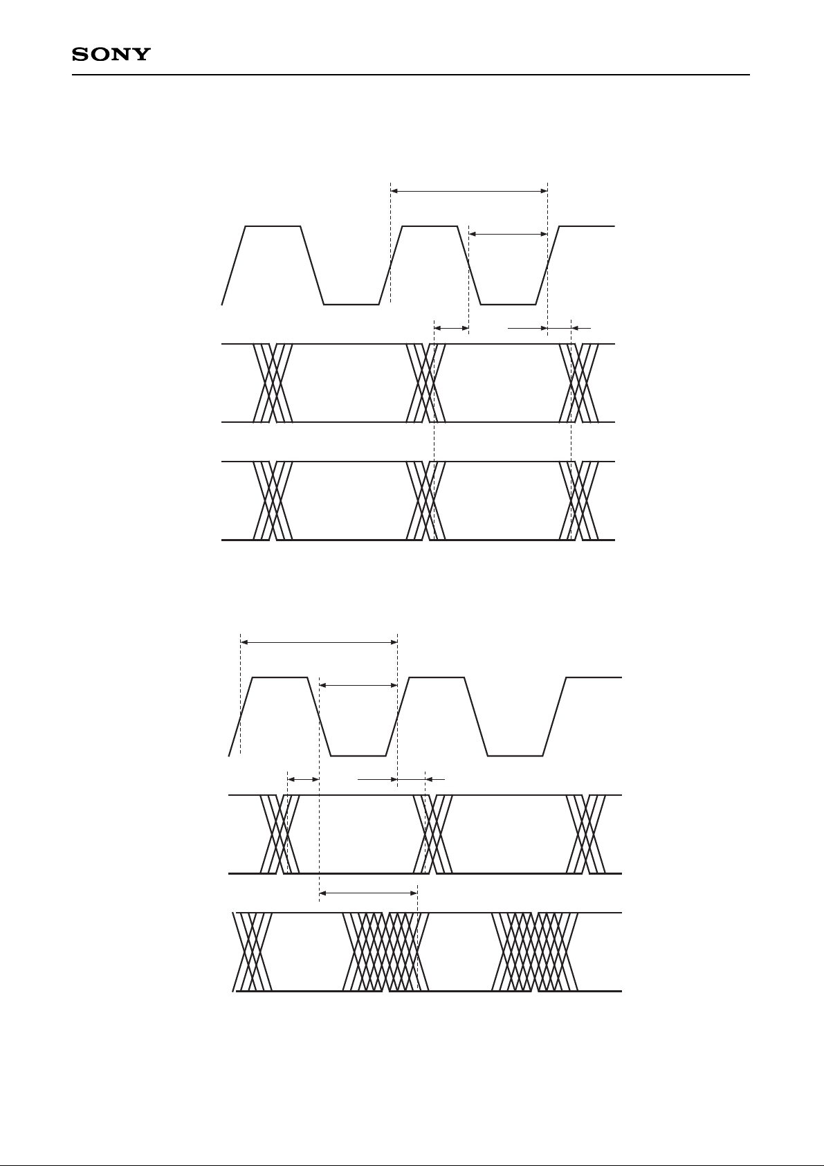
Timing Charts (RAM)
(1) Write mode (XR/W = H)
XRD
T
RD
TCRD
TSRD
A0 to 9
D0 to 9
TPDD
THRD
Note) The address is not latched internally, so do not change the address while XWR is low.
(1) Read mode (XR/W = L)
XWR
T
WR
TCWR
TSWR
A0 to 9
D0 to 9
THWR
Note) The address is not latched internally, so do not change the address while XRD is low.
Page 12
– 12 –
CXA2108Q
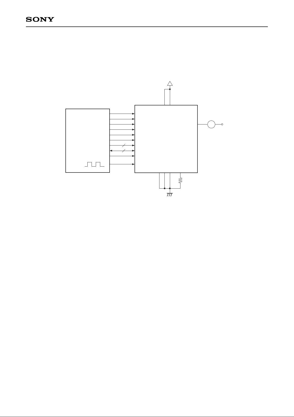
Electrical Characteristics Measurement Circuit
DC Characteristics Measurement Circuit
A
XRST
AVCC
DVCC
5V
1.5V
Logic Tester CXA2108Q
MODE
XR/W IOUT0 to 23
XRD
XWR
DLDI
A0 to 9
D0 to 9
10
0V
5V
15MHz
XCS
CLK
2kΩ
AGND
DGND
IGND
REXT
10
Page 13
– 13 –
CXA2108Q
Description of Operation
1. Description
The CXA2108Q is an LED driver for full color LED displays. The RGB luminance which becomes the video
data is controlled by pulse width modulation (PWM), and the luminance variance of each LED is corrected by
the drive current. The basic PWM clock width can be set in 16 steps from 1× to 16× by the brightness data,
making it possible to adjust the brightness of the entire screen. There are 24 driver outputs, and time division
allows driving of either two or six LEDs per output by adding an external FET or other switch.
The luminance (pulse width), drive current and brightness are set by writing data to the internal memory
according to the memory map. The luminance and drive current can be set independently for each LED.
2. Relationship between the luminance data (PWM data: Dv), brightness data (Db) and the LED emitting duty
The CXA2108Q adjusts the LED luminance which becomes the video data by changing the LED emitting time
duty through PWM of the luminance data. The luminance consists of luminance data and brightness data. The
luminance data (Dv) has an accuracy of 10 bits (= 1,024 steps: 0 to 1,023) and can be set independently for
each LED. The brightness data (Db) controls the basic PWM clock width with 4 bits (= 16 steps: 1× to 16×),
and is common data for all outputs. The brightness data is normally used when adjusting the brightness of the
entire screen.
Labeling the LED emitting cycle as Ts and the CLK cycle as TCLK , this relationship is given by the following
formula.
Ts = 1,024 × 16 × TCLK
The LED emitting time Tv within this Ts time is:
Tv = Dv × Db × TCLK
Therefore, the emitting duty is:
Tv/Ts × 100 = (Dv × Db)/(1,024 × 16) × 100 [%]
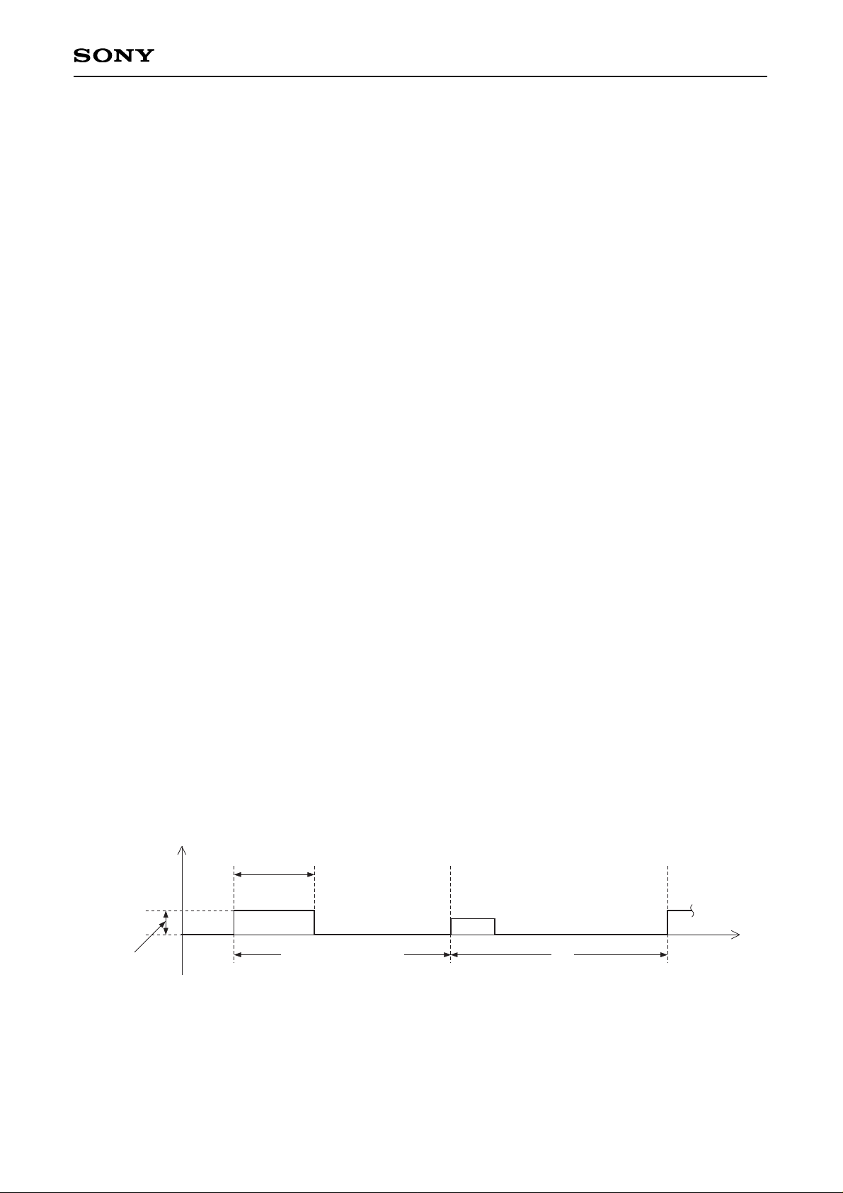
The drive current waveform and the relationship between the luminance data, brightness data and the emitting
duty are shown below.
Current
Drive current
IOUT
0
Tv = Dv × Db × T
CLK
TS = 1,024 × 16 × TCLK
TS
Time
Fig. 1. Drive Current Waveform
Page 14

– 14 –
CXA2108Q
3. Drive current data (Dd)
Even when driving LEDs of the same color with the same current value, individual differences in characteristics
result in an uneven emitting intensity. In addition, the required current value also differs according to the
emitting color (RGB). That is to say, the necessary current differs for each LED. This drive current IOUT
corresponds to the amplitude of the IOUT output PWM waveform as shown in Fig. 1. The CXA2108Q can set
this current independently for each LED using Coarse Adj. (2 bits: D8, D9) and Fine Adj. (8 bits: D0 to D7). The
maximum drive current (Io (FFh): IOUT @ D0 to D7 = FFh) is set by Coarse Adj. (2 bits: D8, D9). The
minimum drive current (Io (00h): IOUT @ D0 to D7 = 00h) is approximately 1/2 of Io (FFh), and the range from
the minimum to the maximum drive current can be set at an accuracy of 8 bits (D0 to D7 = 256 steps).
Note that this drive current is generated using the Iref described in 6. as the reference.
The relationship between the Fine Adj. (8 bits: D0 to D7) data and the drive current, and the drive current data
(D0 to D9) to drive current correspondence table are shown below.
Drive current
D9 D8
0 0
D9 D8
0 1
D9 D8
1 0
D9 D8
1 1
Drive current data (Dd)
D7 to 0
D7 D0
00000000 (00h)
:
10000000 (80h)
:
11111111 (FFh)
400 × Iref
:
600 × Iref
:
800 × Iref
800 × Iref
:
1200 × Iref
:
1600 × Iref
1200 × Iref
:
1800 × Iref
:
2400 × Iref
1600 × Iref
:
2400 × Iref
:
3200 × Iref
Minimum drive current Io (00h)
Maximum drive current Io (FFh)
Table 4. Drive Current Data (D0 to D9) to Drive Current Correspondence Table
Nv∗1and emitting duty
Nv
Brightness (D3 to 0) = 0000
Emitting duty [%]
Luminance data (Dv)
D9 to 0
D9 D0
0000000000
0000000001
0000000010
:
1000000000
:
1111111111
0
1
2
:
512
:
1023
0
0.006
0.012
:
3.125
:
6.244
:
:
Nv
Brightness (D3 to 0) = 0111
Emitting duty [%]
0
8
16
:
4096
:
8184
0
0.049
0.098
:
25.00
:
49.95
Nv
Brightness (D3 to 0) = 1111
Emitting duty [%]
0
16
32
:
8192
:
16368
0
0.098
0.195
:
50.00
:
99.90
Table 3. Relationship Between Luminance Data, Brightness Data and Emitting Duty
∗1
Nv = Tv/TCLK = Dv × Db
Drive current
(Maximum drive current)
(256 steps)
Fine Adj. (8 bits: D0 to D7) data
Io (FFh)
≈ Io (FFh)/2
Io (00h)
0
01h
1 LSB
= (Io (FFh)
– Io (00h))/255
• • • •
00h
FEh
FFh
(Minimum drive current)
Fig. 2. Relationship Between Fine Adj. (8 bits: D0 to D7) Data and Drive Current
Page 15

– 15 –
CXA2108Q
4. Operating modes (Upper/Lower, Upper/Lower/RGB)
The CXA2108Q has the following two operation modes which are set by the MODE pin.
4-1. Upper/Lower mode (MODE = low)
In this mode, two LEDs are driven by time division for each IOUT output.
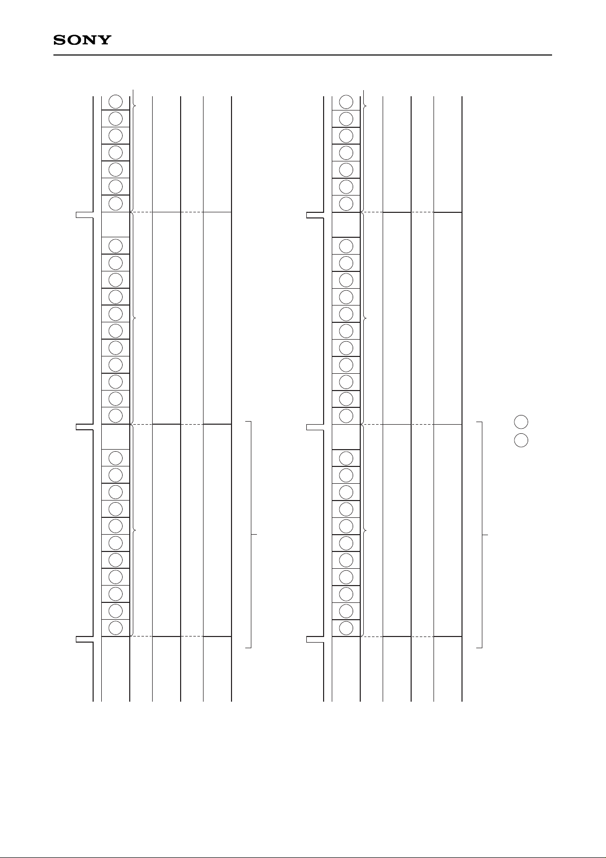
First, PWM waveform output starts triggered by the DLDI input signal. In this mode, two kinds of luminance
data are output by time division for each output. Labeling these data as U and L, the driver outputs the data in
the order of U → L → U → L → U → and so on. The XUPR pin output voltage switches in sync with the LED
emitting cycle Ts in the order of L → H → L → and so on, so this can be used as the FET or other switch signal
for switching the LED. (See Fig. 6. Timing Chart 2-1 and Fig. 11. Application Circuit (1) for details.)
New PWM data is output when the next DLDI signal is input.
4-2. Upper/Lower/RGB mode (MODE = high)
In this mode, six LEDs can be driven by time division for each IOUT output.
PWM waveform output starts triggered by the DLDI input signal. In this mode, six kinds of luminance data are
output by time division for each output. Labeling these data as UB, UR, UG, LB, LR and LG, the driver
switches the output in the order of UB → UR → UG → LB → LR → LG → UB → and so on. Like Upper/Lower
mode, the XUPR and also the XB, XR and XG output voltages switch in sync with Ts, so these can be used as
the FET or other switch signals for switching the LEDs. The output voltages at this time are: XUPR = low for
U∗, XUPR = high for L∗, XB = low (XR = XG = high) for ∗B, XR = low (XB = XG = high) for ∗R, and XG = low
(XB = XR = high) for ∗G. (See Fig. 7. Timing Chart 2-2 and Fig. 12. Application Circuit (2) for details.)
New PWM data is output when the next DLDI signal is input.
5. Luminance data memory and DLDI signal
The CXA2108Q uses two sets of 6-word × 24-channel × 10-bit RAM (RAM (A), RAM (B)) as luminance data
memories, and switches these memories. While the data in one memory is being loaded internally and PWM
output is being performed, the next luminance data can be written to the other memory from an external
source. Memory switching is performed by inputting a trigger signal to the DLDI pin. The read/write enabled
memory alternates from A → B → A → and so on, and the memory used for PWM output alternates from B →
A → B → and so on each time the signal is input to DLDI. The DLDI signal switches the memory, and at the
same time functions as the PWM output start trigger pulse. See the Timing Charts for details.
6. Reference current (Iref)
The drive current is generated using the current flowing to an external resistor as the reference. This resistor
Rext is connected between the REXT pin and GND. The REXT pin voltage is designed to be unaffected by
supply voltage, temperature or other fluctuations, and is always a constant voltage (approximately 1.3V).
Therefore, a constant current can be realized by using a resistor that does not have temperature
characteristics. The current obtained by dividing this current value by the number of IOUT outputs (24) is
defined as Iref.
Iref = (1.3/Rext)/24
The maximum drive current value can be changed by varying the resistance value. See Table 2. Drive Current
Setting and Power Consumption for details.
Page 16

– 16 –
CXA2108Q
7. Data setting
The above mentioned luminance data Dv, brightness data Db and drive current data Dd are set using address
input pins A0 to A9 and data I/O pins D0 to D9. See the Timing Charts for the memory read/write enabled
period, and Table 1. Read/Write Switching Condition Correspondence Table for the pin setting conditions. The
address, data, XWR and XRD setup, hold and other timings should be as stated in the Electrical
Characteristics. See Tables 5. and 6. LED Driver Memory Map with respect to the memory address of each
IOUT output pin (IOUT0 to IOUT23).
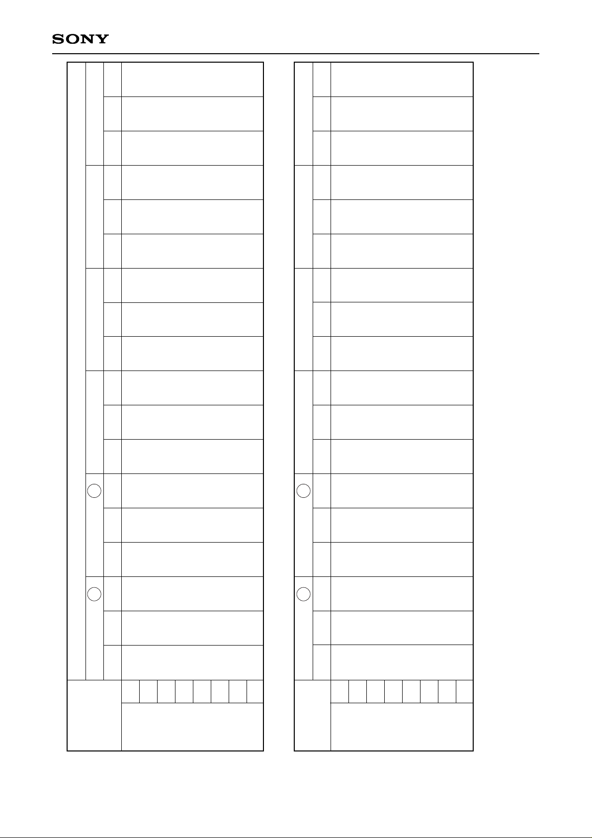
The relationship between the data and the memory address is as follows.
Brightness Data
0100101000
0100100111
LG
LR
LB
UG
UR
UB
Upper/Lower/RGB
Can't use
Brightness Data
L
IOUT0
IOUT1
IOUT2
IOUT3
IOUT4
IOUT23
a + 23
a
IOUT21
IOUT22
U
Upper/Lower
Can't use
0100100000
0100011111
0010010000
0010001111
0001111000
0001110111
0001100000
0001011111
0001001000
0001000111
0000110000
0000101111
0000011000
0000010111
0000000000
MODE
Don't use
Don't use
•
•
•
•
•
•
•
•
•
•
•
•
•
•
•
•
•
•
•
•
Fig. 3. Relationship Between Memory Address and Data (Luminance Data Dv, Brightness Data Db)
A9 to A0
MSB LSB
A9 A0
Page 17

– 17 –
CXA2108Q
LG
LR
LB
UG
UR
UB
Upper/Lower/RGB
Can't use
L
IOUT0
IOUT1
IOUT2
IOUT3
IOUT4
IOUT23
a + 23
a
IOUT21
IOUT22
U
Upper/Lower
Can't use
1010010000
1010001111
1001111000
1001110111
1001100000
1001011111
1001001000
1001000111
1000110000
1000101111
1000011000
1000010111
1000000000
MODE
•
•
•
•
•
•
•
•
•
•
•
•
•
•
•
•
Fig. 4. Relationship Between Memory Address and Data (Drive Current Data Dd)
A9 to A0
MSB LSB
A9 A0
Page 18
– 18 –
CXA2108Q
IOUT0
IOUT1
IOUT2
IOUT3
IOUT4
IOUT5
IOUT6
IOUT7
IOUT8
IOUT9
IOUT10
IOUT11
IOUT12
IOUT13
IOUT14
IOUT15
IOUT16
IOUT17
IOUT18
IOUT19
IOUT20
IOUT21
IOUT22
IOUT23
IOUT0
IOUT1
IOUT2
IOUT3
IOUT4
IOUT5
IOUT6
IOUT7
IOUT8
IOUT9
IOUT10
IOUT11
IOUT12
IOUT13
IOUT14
IOUT15
IOUT16
IOUT17
IOUT18
IOUT19
IOUT20
IOUT21
IOUT22
IOUT23
0000000 0000001 0000010 0000011 0000100 0000101 0000110 0000111 0001000 0001001 0001010 0001011 0001100 0001101 0001110 0001111 0010000 0010001
A9 to A3
UPPER LOWER
A2 to A0
000
001
010
011
100
101
110
111
IOUT0
IOUT1
IOUT2
IOUT3
IOUT4
IOUT5
IOUT6
IOUT7
IOUT8
IOUT9
IOUT10
IOUT11
IOUT12
IOUT13
IOUT14
IOUT15
IOUT16
IOUT17
IOUT18
IOUT19
IOUT20
IOUT21
IOUT22
IOUT23
IOUT0
IOUT1
IOUT2
IOUT3
IOUT4
IOUT5
IOUT6
IOUT7
IOUT8
IOUT9
IOUT10
IOUT11
IOUT12
IOUT13
IOUT14
IOUT15
IOUT16
IOUT17
IOUT18
IOUT19
IOUT20
IOUT21
IOUT22
IOUT23
1000000 1000001 1000010 1000011 1000100 1000101 1000110 1000111 1001000 1001001 1001010 1001011 1001100 1001101 1001110 1001111 1010000 1010001
UPPER LOWER
A2 to A0
000
001
010
011
100
101
110
111
Luminance Data
Drive Current Data
Brightness data: A9 to A3 = 0100100b (24h) A2 to A0 = Don't care
Table 5. LED Driver Memory Map (Upper/Lower mode)
LUL
U
Page 19

– 19 –
CXA2108Q
IOUT0
IOUT1
IOUT2
IOUT3
IOUT4
IOUT5
IOUT6
IOUT7
IOUT8
IOUT9
IOUT10
IOUT11
IOUT12
IOUT13
IOUT14
IOUT15
IOUT16
IOUT17
IOUT18
IOUT19
IOUT20
IOUT21
IOUT22
IOUT23
IOUT0
IOUT1
IOUT2
IOUT3
IOUT4
IOUT5
IOUT6
IOUT7
IOUT8
IOUT9
IOUT10
IOUT11
IOUT12
IOUT13
IOUT14
IOUT15
IOUT16
IOUT17
IOUT18
IOUT19
IOUT20
IOUT21
IOUT22
IOUT23
IOUT0
IOUT1
IOUT2
IOUT3
IOUT4
IOUT5
IOUT6
IOUT7
IOUT8
IOUT9
IOUT10
IOUT11
IOUT12
IOUT13
IOUT14
IOUT15
IOUT16
IOUT17
IOUT18
IOUT19
IOUT20
IOUT21
IOUT22
IOUT23
IOUT0
IOUT1
IOUT2
IOUT3
IOUT4
IOUT5
IOUT6
IOUT7
IOUT8
IOUT9
IOUT10
IOUT11
IOUT12
IOUT13
IOUT14
IOUT15
IOUT16
IOUT17
IOUT18
IOUT19
IOUT20
IOUT21
IOUT22
IOUT23
IOUT0
IOUT1
IOUT2
IOUT3
IOUT4
IOUT5
IOUT6
IOUT7
IOUT8
IOUT9
IOUT10
IOUT11
IOUT12
IOUT13
IOUT14
IOUT15
IOUT16
IOUT17
IOUT18
IOUT19
IOUT20
IOUT21
IOUT22
IOUT23
IOUT0
IOUT1
IOUT2
IOUT3
IOUT4
IOUT5
IOUT6
IOUT7
IOUT8
IOUT9
IOUT10
IOUT11
IOUT12
IOUT13
IOUT14
IOUT15
IOUT16
IOUT17
IOUT18
IOUT19
IOUT20
IOUT21
IOUT22
IOUT23
0000000 0000001 0000010 0000011 0000100 0000101 0000110 0000111 0001000 0001001 0001010 0001011 0001100 0001101 0001110 0001111 0010000 0010001
A9 to A3
B R
UPPER
G B R
LOWER
G
A2 to A0
000
001
010
011
100
101
110
111
IOUT0
IOUT1
IOUT2
IOUT3
IOUT4
IOUT5
IOUT6
IOUT7
IOUT8
IOUT9
IOUT10
IOUT11
IOUT12
IOUT13
IOUT14
IOUT15
IOUT16
IOUT17
IOUT18
IOUT19
IOUT20
IOUT21
IOUT22
IOUT23
IOUT0
IOUT1
IOUT2
IOUT3
IOUT4
IOUT5
IOUT6
IOUT7
IOUT8
IOUT9
IOUT10
IOUT11
IOUT12
IOUT13
IOUT14
IOUT15
IOUT16
IOUT17
IOUT18
IOUT19
IOUT20
IOUT21
IOUT22
IOUT23
IOUT0
IOUT1
IOUT2
IOUT3
IOUT4
IOUT5
IOUT6
IOUT7
IOUT8
IOUT9
IOUT10
IOUT11
IOUT12
IOUT13
IOUT14
IOUT15
IOUT16
IOUT17
IOUT18
IOUT19
IOUT20
IOUT21
IOUT22
IOUT23
IOUT0
IOUT1
IOUT2
IOUT3
IOUT4
IOUT5
IOUT6
IOUT7
IOUT8
IOUT9
IOUT10
IOUT11
IOUT12
IOUT13
IOUT14
IOUT15
IOUT16
IOUT17
IOUT18
IOUT19
IOUT20
IOUT21
IOUT22
IOUT23
IOUT0
IOUT1
IOUT2
IOUT3
IOUT4
IOUT5
IOUT6
IOUT7
IOUT8
IOUT9
IOUT10
IOUT11
IOUT12
IOUT13
IOUT14
IOUT15
IOUT16
IOUT17
IOUT18
IOUT19
IOUT20
IOUT21
IOUT22
IOUT23
IOUT0
IOUT1
IOUT2
IOUT3
IOUT4
IOUT5
IOUT6
IOUT7
IOUT8
IOUT9
IOUT10
IOUT11
IOUT12
IOUT13
IOUT14
IOUT15
IOUT16
IOUT17
IOUT18
IOUT19
IOUT20
IOUT21
IOUT22
IOUT23
1000000 1000001 1000010 1000011 1000100 1000101 1000110 1000111 1001000 1001001 1001010 1001011 1001100 1001101 1001110 1001111 1010000 1010001
B R
UPPER
G B
LOWER
R G
A2 to A0
000
001
010
011
100
101
110
111
Luminance Data
Drive Current Data
Brightness data: A9 to A3 = 0100100b (24h) A2 to A0 = Don't care
Table 6. LED Driver Memory Map (Upper/Lower/RGB mode)
LG
LR
LB
UG
UR
UB
UG
UR
UB
LG
LR
LB
Page 20
– 20 –
CXA2108Q
U L U L U L U
RAM (A)
R/W Disable
(Accessing Internally)RAM (A)
RAM (B)
DLDI
IOUT
output data
Partial enlargement diagram (Fig. 6. Timing Chart 2-1)
R/W Enable R/W DisableR/W Enable
R/W EnableR/W Enable
L U L U • • • U L
R/W Disable
(Accessing Internally)
U L U L U L U L U • • • U L U L U L U
RAM (B) RAM (A)
UB UR UG LB LR LG UB
RAM (A)
R/W Disable
(Accessing Internally)RAM (A)
RAM (B)
DLDI
IOUT
output data
Partial enlargement diagram (Fig. 7. Timing Chart 2-2)
R/W Enable R/W DisableR/W Enable
R/W EnableR/W Enable
UR UG LB LR • • • UB UR
R/W Disable
(Accessing Internally)
UG LB LR LG UB UR UG LB LR • • • UB UR UG LB LR LG UB
RAM (B) RAM (A)
Note) U , L and other symbols correspond to Tables 5. and 6. LED Driver Memory Map.
Fig. 5. Timing Chart 1. Relationship between PWM waveform output and luminance RAM (A)/(B) with respect to DLDI input pulse
Case 1: Upper/Lower mode
Case 2: Upper/Lower/RGB mode
– 21 –
Page 21

CXA2108Q
DLDI
DLDO
RDY
IOUT
XUPR
Partial enlargement diagram (Fig. 8. Timing Chart 3-1)
1 clk
1024 × 16 clk = 1 Cycle
U
Emitting start Emitting end
L U L U L U
Note) U , L and other symbols correspond to Tables 5. LED Driver Memory Map.
Fig. 6. Timing Chart 2-1. DLDI input to IOUT output (Upper/Lower mode)
Page 22

– 22 –
CXA2108Q
Fig. 7. Timing Chart 2-2. DLDI input to IOUT output (Upper/Lower/RGB mode)
DLDI
DLDO
RDY
IOUT
XUPR
Partial enlargement diagram (Fig. 9. Timing Chart 3-2)
1 clk
1024 × 16 clk = 1 Cycle
XB
XR
XG
UB
Emitting start Emitting end
UR UG LB LR LG UB
Note) UB , LG and other symbols correspond to Tables 6. LED Driver Memory Map.
Page 23

– 23 –
CXA2108Q
48 clk 9 clk
8 clk
48 clk
XUPR
RDY
DLDO
DLDI
CLK
Nv clk
Emitting start Emitting start
Luminance data RAM (A)
E = R/W Enable
D = R/W Disable
IOUT
Luminance data RAM (B)
Driver current RAM
Emitting end
∗
NV = Dv × Db (Dv: Luminance data, Db: Brightness data)
E
D
D
E
ED D E
E
1024 × 16 clk = 1 Cycle
Fig. 8. Timing Chart 3-1. DLDI input to IOUT output (1 cycle) example (Upper/Lower mode)
Page 24

– 24 –
CXA2108Q
Fig. 9. Timing Chart 3-2. DLDI input to IOUT output (1 cycle) example (Upper/Lower/RGB mode)
48 clk 9 clk
8 clk
48 clk
XUPR
RDY
DLDO
DLDI
CLK
Nv clk
Emitting start Emitting start
Luminance data RAM (A)
E = R/W Enable
D = R/W Disable
IOUT
XG
XR
XB
Luminance data RAM (B)
Driver current RAM
Emitting end
∗
NV = Dv × Db (Dv: Luminance data, Db: Brightness data)
E
D
D
E
ED D E
E
1024 × 16 clk = 1 Cycle
Page 25
– 25 –
CXA2108Q
,
,
1 clk = 15MHz (Max)
128 clk 48 clk 9 clk
8 clk
Nv clk
Emitting start
Luminance data write
Luminance data RAM (A)
IOUT
E = R/W Enable
D = R/W Disable
XUPR
RDY
WALL
DLDO
DLDI
D0 to 9
A0 to 9
XR/W
XWR
XRST
CLK
Luminance data RAM (B)
Driver current RAM
Brightness data write
Emitting end
1 clk = 7.5MHz (Max)
,
,
,
,
,
,
,
,
,
,
,
,
201 202 22F 120 000 001 002
Dd1 Dd2
Dd2F
Db Dv0 Dv1 Dv2
Drive current data write
∗
NV = Dv × Db (Dv: Luminance data, Db: Brightness data)
∗
Dd: Drive current data
IC initialization
D E
D
ED D
D
E
E
02F
Dv2F
Dd0
200
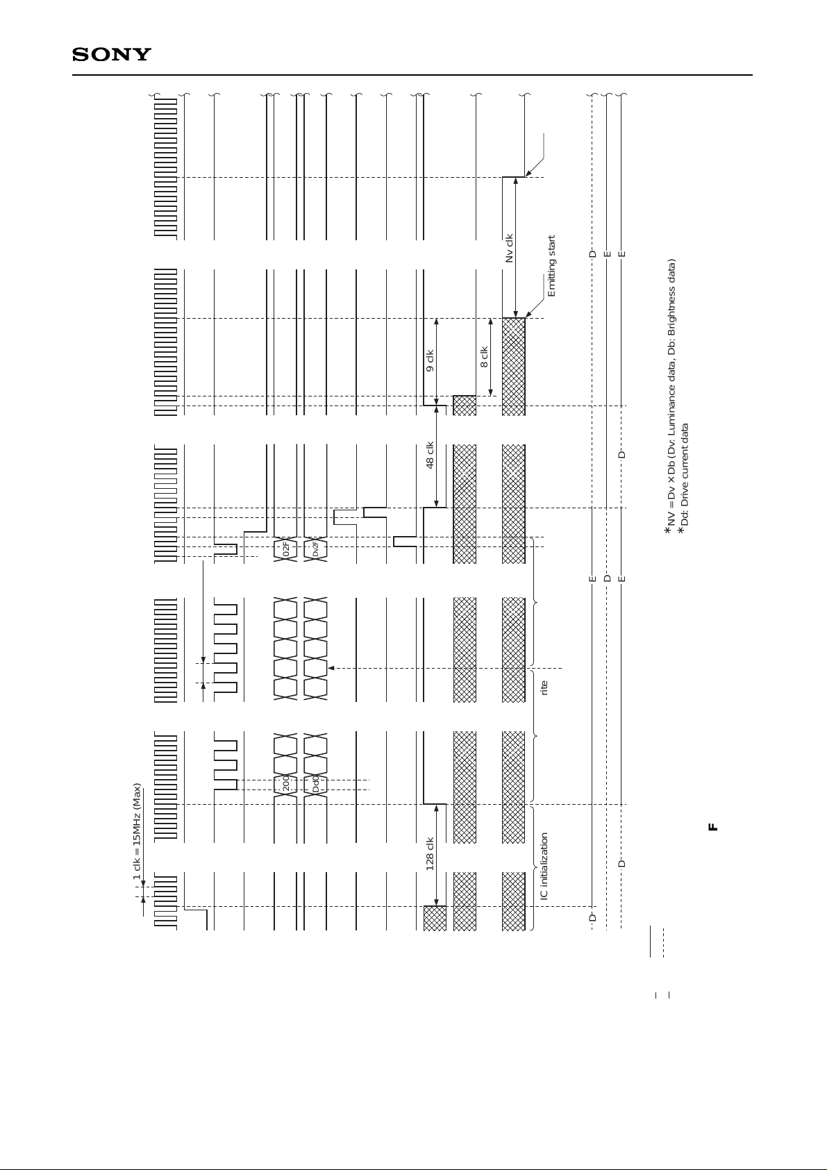
Fig. 10. Timing Chart 4. XRST input to IOUT output example (Upper/Lower mode)
Page 26

– 26 –
CXA2108Q
25 26 27 28 29 30 31 32 33 34 35 36 37 38 39
40
45
46
47
48
49
50
51
52
53
54
55
56
57
58
59
60
61
62
63
64
65666768697071727374757677787980
123456789
10
111213
141516
17
181920
IOUT5
IOUT4
IOUT3
IOUT2
IOUT1
IOUT0
AV
CC
AGND
Bus CLK
(7.5MHz)
REXT
Read/Write
Control signal
Address: A0 to A9
From Address Bus
2kΩ
XR/W
XRD
XWR
41
42
43
44
IOUT18
IOUT19
IOUT20
IOUT21
IOUT22
IOUT23
MODE
212223
24
15MHz CLK
XUPR
IOUT17
IOUT16
IOUT15
IOUT14
IOUT13
IOUT12
IOUT11
IOUT10
IOUT9
IOUT8
IOUT7
IOUT6
AGND
IGND
IGND IGND IGND IGND
DVCC
DGND
Data: D0 to D9
From Data Bus
DVCC
DGND
IGND
AGND
DGND
DGND
AVCC
Address
Bus
Bus CLK
Data Bus
7.5MHz
5V0V5V0V5V
0V
VG, VR, VB: LED DC supply
VG = 5.5V VR = 4.0V VB = 5.5V
G
G
G
Green
B
B
from XUPR
from IOUT23
from IOUT3
from IOUT2
from IOUT1
from IOUT0
R
Red
B
Bule
•••••••••
Application Circuit
UPPER/LOWER mode
Fig. 11. Application Circuit (1)
Application circuits shown are typical examples illustrating the operation of the devices. Sony cannot assume responsibility for
any problems arising out of the use of these circuits or for any infringement of third party patent and other right due to same.
Page 27

– 27 –
CXA2108Q
25 26 27 28 29 30 31 32 33 34 35 36 37 38 39 40
45
46
47
48
49
50
51
52
53
54
55
56
57
58
59
60
61
62
63
64
65666768697071727374757677787980
12345
678
9
101112
131415
16
171819
20
IOUT5
IOUT4
IOUT3
IOUT2
IOUT1
IOUT0
AV
CC
AGND
Bus CLK
(7.5MHz)
REXT
Address: A0 to A9
From Address Bus
2kΩ
XR/W
XRD
XWR
41
42
43
44
IOUT18
IOUT19
IOUT20
IOUT21
IOUT22
IOUT23
MODE
212223
24
15MHz CLK
XUPR
XB
XR
XG
IOUT17
IOUT16
IOUT15
IOUT14
IOUT13
IOUT12
IOUT11
IOUT10
IOUT9
IOUT8
IOUT7
IOUT6
AGND
IGND
IGND IGND IGND IGND
DVCC
DGND
Data: D0 to D9
From Data Bus
DVCC
DGND
DVCC
IGND
AGND
DGND
AVCC
Address
Bus
Bus CLK
Data Bus
7.5MHz
5V0V5V0V5V
0V
Read/write
control signal
VG, VR, VB: LED DC supply
VG = 5.5V VR = 4.0V VB = 5.5V
G
G
G
G
G
Green
B
B
B
B
B
from XUPR
from XG
from XR
from IOUT23
from IOUT1
R
R
R
R
R
Red
Bule
•••••••••
from XB
from IOUT0
UPPER/LOWER/RGB mode
Fig. 12. Application Circuit (2)
Application circuits shown are typical examples illustrating the operation of the devices. Sony cannot assume responsibility for
any problems arising out of the use of these circuits or for any infringement of third party patent and other right due to same.
Page 28

– 28 –
CXA2108Q
Package Outline Unit: mm
PACKAGE STRUCTURE
SONY CODE
EIAJ CODE
JEDEC CODE
QFP-80P-L01
QFP080-P-1420
PACKAGE MATERIAL
LEAD TREATMENT
LEAD MATERIAL
PACKAGE MASS
EPOXY RESIN
SOLDER PLATING
42/COPPER ALLOY
1.6g
23.9 ± 0.4
20.0 – 0.1
+ 0.4
1
80
65
64
41
40
25
24
0.8
0.35 – 0.1
+ 0.15
14.0 – 0.1
+ 0.4
17.9 ± 0.4
16.3
0.1 – 0.05
+ 0.2
2.75 – 0.15
+ 0.35
0.8 ± 0.2
0.15 – 0.05
+ 0.1
80PIN QFP (PLASTIC)
M
0.2
0.15
0° to 10°
DETAIL A
A
 Loading...