

Page 1

EIAJ Sound Multiplexing Decoder
Description
The CXA2013M is a bipolar IC designed as EIAJ
TV sound multiplexing decoder, provides various
functions including sound multiplexing demodulation,
broadcast mode identification (stereo/bilingual
discrimination display), volume, tone control and
muting.
Features
• Adjustment free of filter
• Audio multiplexing decoder
• Sound processor
— One external input
— Bass control
— Treble control
— V olume control
— Balance control
are all included in a single chip. Almost any sort of
signal processing is possible through this IC.
• Separation adjustment, each mode control and sound
processor control are possible through I2C BUS.
CXA2013M
30 pin SOP (Plastic)
Absolute Maximum Ratings (Ta = 25°C)
• Supply voltage VCC 12 V
• Operating temperature Topr –20 to +75 °C
• Storage temperature Tstg –65 to +150 °C
• Allowable power dissipation PD 1000 mW
Operating Supply Voltage Range 8.5 to 9.5 V
Applications
TVs
Structure
Bipolar silicon monolithic IC
Pin Configuration
SC OUT
NC
SC IN
MC OUT
MC IN
TV OUT-L
TV OUT-RNCAUX-L
30
29
28
27
26
25
24
23
1
2
3
4
5
6
7
8
REFL
Vcc
MPX IN
GND
SUBI
Sony reserves the right to change products and specifications without prior notice. This information does not convey any license by
any implication or otherwise under any patents or other right. Application circuits shown, if any, are typical examples illustrating the
operation of the devices. Sony cannot assume responsibility for any problems arising out of the use of these circuits.
CUBI
NC
SDA
22
9
SCL
AUX-R
21
10
DGND
CL-R
20
11
BAL
CL-L
19
12
TRE
CH-R
18
13
BASS
CH-L
171516
14
VOL
LS OUT-L
LS OUT-R
– 1 –
E00Y28A1Y-PS
Page 2

Block Diagram
– 2 –
SUBI
1
BIAS
CURRENT
IBIAS
2
SC OUT
30
SUBDEEM
FM
DEMOD
BUFFER
VOLTAGE
REGULATOR
SC IN
28
BIAS
VOLTAGE
3
MC OUT
27
MAINDEEM
4
26
VCA
MC IN
SUB
DET
SUB
BPF
4.5fH
TRAP
SUB
ATT
MPX SIGNAL
5
TV OUT-L24TV OUT-R21AUX-R22AUX-L17CH-L19CL-L
25
MATRIX SW
MAIN
IIL LOGIC & CONT
3.5f
3.5fH
VCO
H
CLOCK
952Hz
BPF
CUE
BPF
CUE
CARRIOR
AM
DEMOD
952Hz
CLOCK
COMP
6
TONE
BASS
TRE
TONE
18
20
VCA
VOL
BAL
VCA
DAC BUS DEC
11
12
13
14
LS OUT-L
16
LS OUT-R
15
8
9
10
GND
REFL
Vcc
MPX IN
CUBI
CH-R
CL-R
BAL
TRE
BASS
VOL
SDA
SCL
DGND
CXA2013M
Page 3
CXA2013M
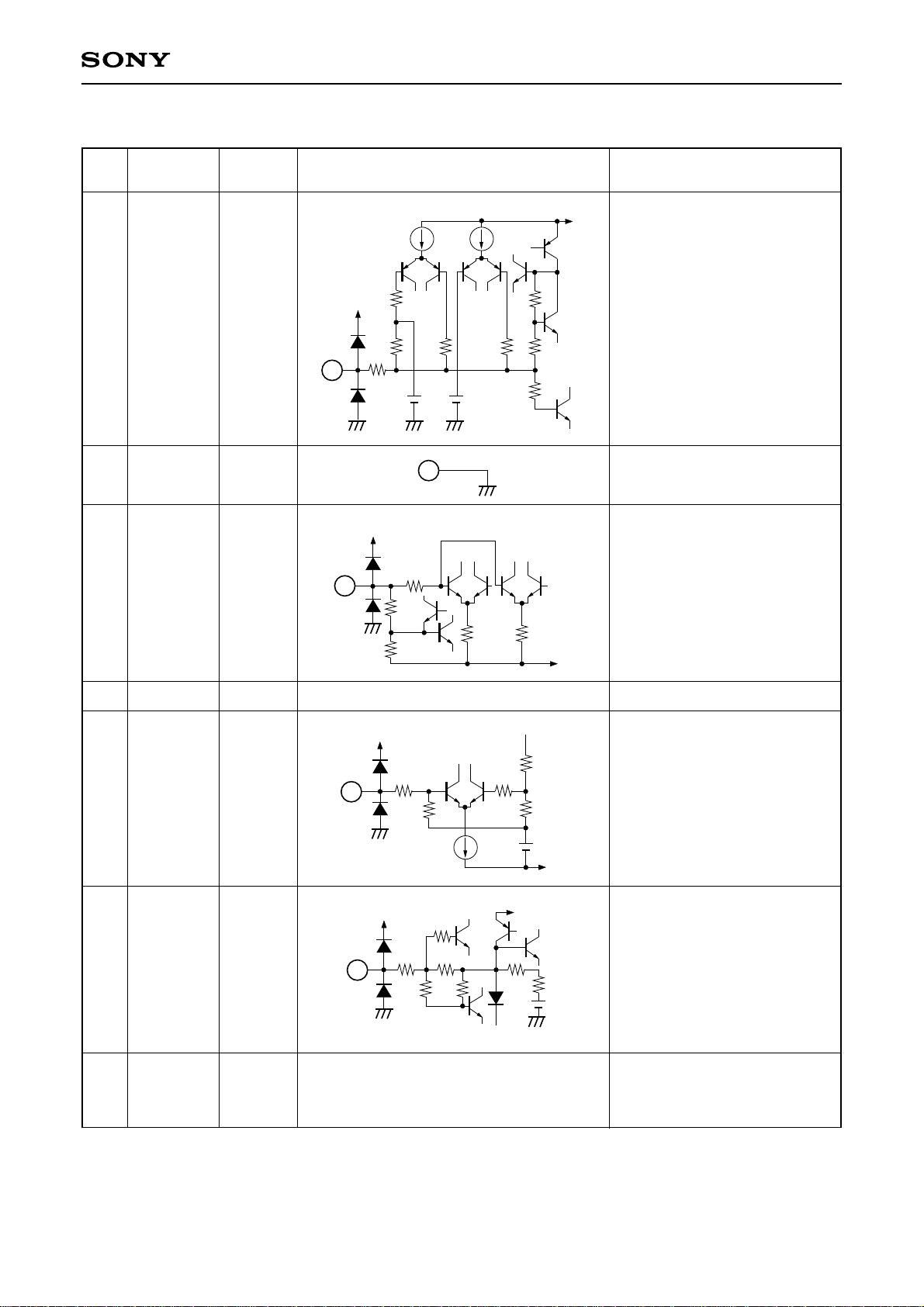
Pin Description (Ta = 25°C, VCC = 9V)
Pin
No.
Symbol
Pin
voltage
1 SUBI 4.1V
2 GND 0
3 REFL
1.2V
Equivalent circuit Description
Vcc
20µ
64k
Bias capacitor connection of
Vcc
80µ
16k
sub FM detector
4.2V
147
3.3k
24k
1k
2
8k
147
1.7V
20k 20k
8k
Analog block GND
The noise elimination filter
connection of internal
reference voltage
GND
16k
1
147
Vcc
3
4VCC —
5 MPX IN 4.1V
6 CUBI
4.1V
7,
23,
NC
29
—
Power supply
Vcc
147
5
50k
80µ
Vcc
6
147
40k
1k
40k
40k
—
27.6k
11k
Vcc
87.9k
30k
4.2V
GND
2k
4.2V
Sound multiplexing signal input.
Typical input level = 110mVrms
(monoural 100%)
Bias capacitor connection of
Cue pulse generator
—
– 3 –
Page 4
CXA2013M
Pin
No.
Symbol
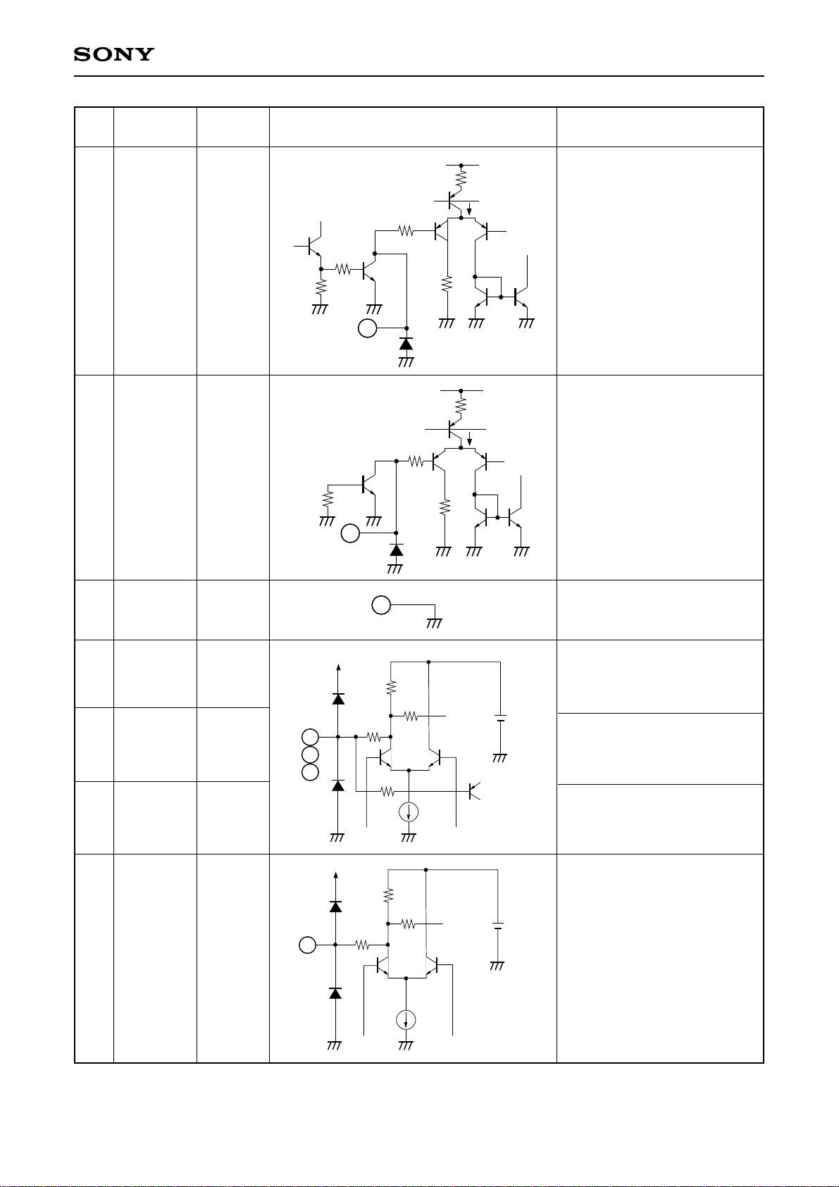
8SDA
9 SCL
Pin
voltage
—
—
7.5k
10.5k
Equivalent circuit Description
V
CC
7.5k
35µ
7.5k
35µ
2.1V
2.1V
Serial data I/O pin
VIH > 3.0V
VIL < 1.5V
Serial clock I/O pin
×2
4.5k
4k
×5
8
4k
3k
V
CC
VIH > 3.0V
×4
3k
VIL < 1.5V
10 DGND
—
11 BAL 4.2V
12 TRE 4.2V
13 BASS 4.2V
14 VOL 5.2V
14
11
12
13
VCC
VCC
9
10
Digital block GND
DAC output pin. (BAL)
Connect LPF capacitance of DAC.
Internal impedance is
approximately 20kΩ.
DAC output pin. (TRE)
2k
40k
20k
5.2V
Connect LPF capacitance of DAC.
Internal impedance is
2k
approximately 20kΩ.
DAC output pin. (BASS)
75µ
Connect LPF capacitance of DAC.
Internal impedance is
approximately 20kΩ.
10k
5k
2k
5.2V
DAC output pin. (VOL)
Connect LPF capacitance of DAC.
×4
×4
Internal impedance is
approximately 5kΩ.
300µ
– 4 –
Page 5

CXA2013M
Pin
No.
15 4.2V
16 4.2V
Symbol
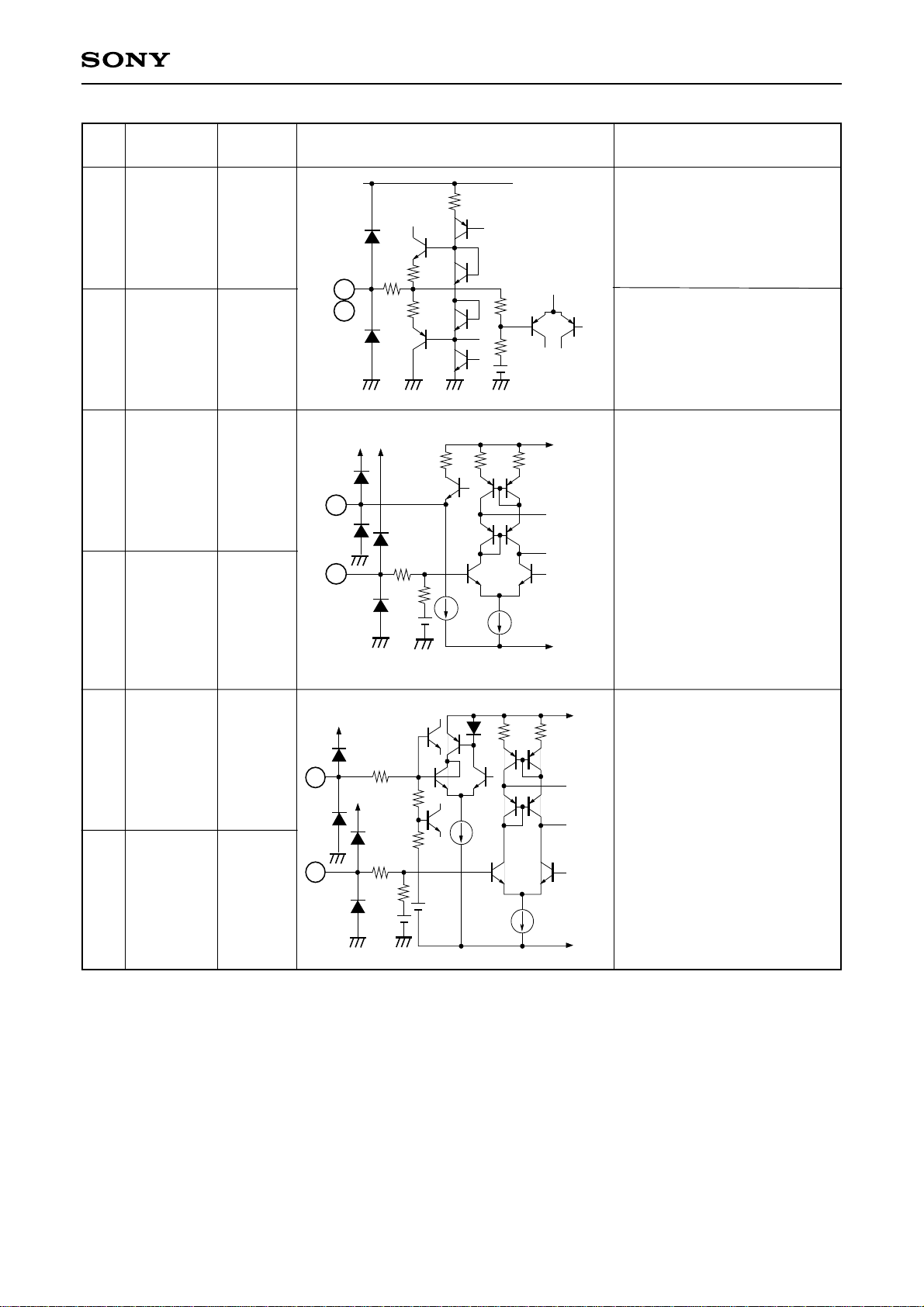
LS OUT-R
LS OUT-L
Pin
voltage
17 CH-L 4.2V
18 CH-R
4.2V
17
18
Equivalent circuit Description
CC
V
3k
LSOUT right channel output
pin
10p
500
15
16
147
500
84k
LSOUT left channel output
pin
Vcc
250µ
250µ
Treble filter pin
(Left channel)
5.7k
147
6k
5.7k
Treble filter pin
(Right channel)
19 CL-L 4.2V
20 CL-R 4.2V
21 AUX-R 4.2V
22 AUX-L 4.2V
21
22
19
20
10.7k
147
147
250µ
36k
12k
4.2V
5.4k
250µ
12.3k
10µ
Vcc
4.2V
Vcc
Bass filter pin
(Left channel)
Bass filter pin
(Right channel)
Right channel external input
pin
Left channel external input
pin
– 5 –
Page 6
CXA2013M
Pin
No.
Symbol
Pin
voltage
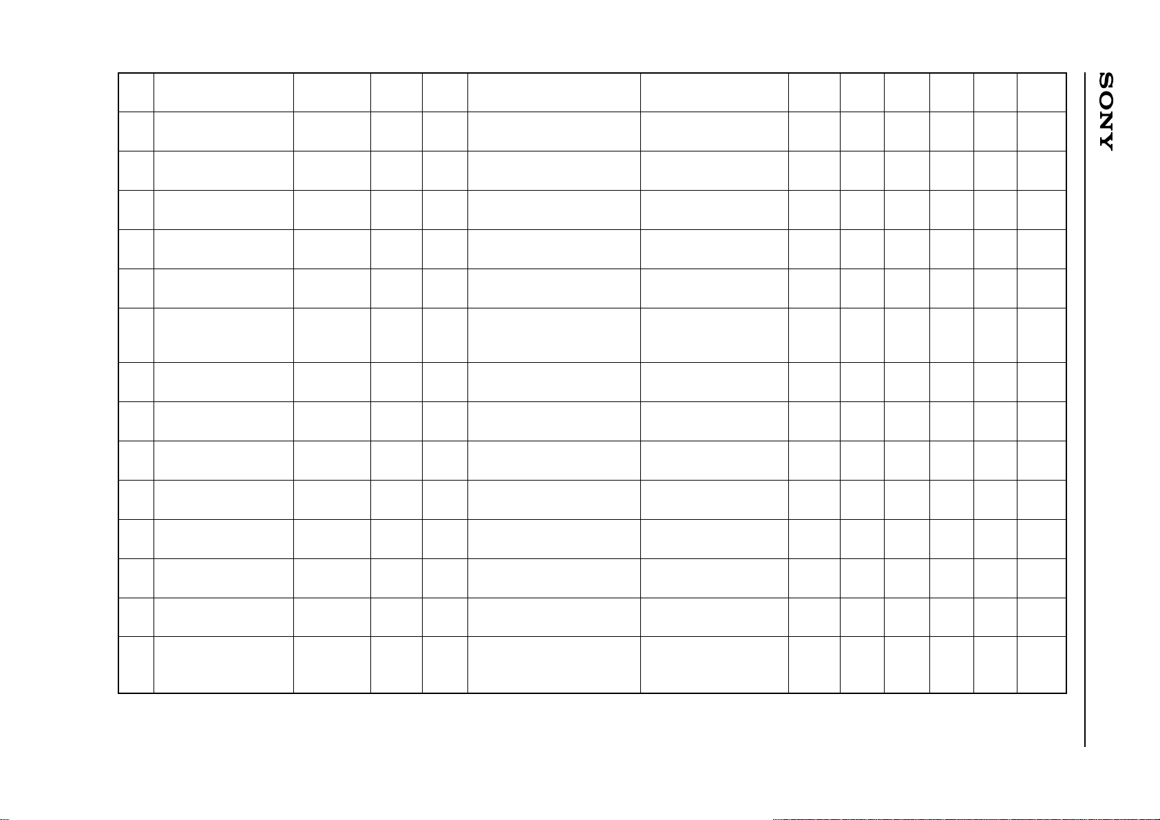
24 TV OUT-R 4.2V
25 TV OUT-L 4.2V
26 MC IN 4.1V
27 MC OUT 3.4V
24
25
27
26
Equivalent circuit Description
V
CC
3k
TVOUT right channel output
pin
580
147
14.3k
35.7k
4.2V
TVOUT left channel output
pin
Vcc
Vcc Vcc
580
147
8k 8k
DC cut capacitor connection
147
16k
4.2V
160µ
80µ
GND
of main signal
28 SC IN 4.1V
30 SC OUT 3.9V
30
28
Vcc
Vcc
147
147
16k
4.2V
8k
40k
4.2V
320µ
Vcc
8k8k
DC cut capacitor connection
of sub signal
80µ
GND
– 6 –
Page 7

Electrical Characteristics
(Ta = 25°C, V
CC = 9V)
No. Item Symbol Mode Input signal
Current consumption
1
MPX input level
2
MPX input level
3
range
MONO output level
4
MONO frequency
5
response
MONO distortion
6
Icc
Vin
Vrange
Vmain
Fcmain
THDm
MONO
MONO
MONO
– 7 –
MONO distortion at
7
maximum input
MONO S/N
8
Sub output level
9
Sub frequency
10
response
THDmmax
SNmain
Vsub
Fcsub
MONO
MONO
BIL
BIL
Input
pin
—
5
—
5
5
5
5
5
5
5
No input
MONO 1kHz, 100% mod.
MONO 1kHz 100% mod.
Sub: Career OFF, Cue: OFF
MONO 10kHz 100% mod.
Sub: Career OFF, Cue: OFF
MONO 1kHz 100% mod.
Sub: Career OFF, Cue: OFF
MONO 1kHz 300% mod.
Sub: Career OFF, Cue: OFF
MONO 1kHz 100% mod.
Sub: Career OFF, Cue: OFF
SUB 1kHz 100% mod.
Main 0% mod., Cue: BIL
SUB 10kHz 100% mod.
Main 0% mod., Cue: BIL
—
Measurement
conditions
20 log ('10k'/'1k')
20 log ('100%'/'0%')
20 log ('10k'/'1k')
Filter
15kLPF
15kLPF
15kLPF
15kLPF
15kLPF
Output
pin
4
5
—
24/25
24/25
24/25
24/25
24/25
24/25
24/25
Min. Typ. Max. Unit
30
—
–3
400
–15.4
—
—
65
400
–18.4
43
110
—
500
–13.4
0.2
0.3
73
500
–15.9
60
—
3
600
–11.4
1.0
2.0
—
600
–13.4
mA
mVrms
mVrms
mVrms
dB
dB
%
%
dB
dB
Sub distortion
11
Sub S/N
12
ST output level L-ch
13
ST output level R-ch
14
THDsub
SNsub
Vstl
Vstr
BIL
BIL
ST
ST
SUB 1kHz 100% mod.
5
Main 0% mod., Cue: BIL
SUB 1kHz 100% mod.
5
Main 0% mod., Cue: BIL
ST-L 1kHz 100% mod.
5
Cue: Stereo
ST-R 1kHz 100% mod.
5
Cue: Stereo
20 log ('100%'/'0%')
15kLPF
15kLPF
15kLPF
15kLPF
24/25
24/25
25
24
—
59
400
400
1.0
64
500
500
2.0
—
600
600
%
dB
mVrms
mVrms
CXA2013M
Page 8

Input
pin
Measurement
conditions
FilterNo. Item Symbol Mode Input signal
Output
pin
Min. Typ. Max. Unit
15
ST distortion L-ch
16
ST distortion R-ch
ST separation
17
L → R
ST separation
18
R → L
Cross talk
19
Main → Sub
Cross talk
20
Sub → Main
Cross talk
21
Main → Sub BOTH mode
– 8 –
Cross talk
22
Sub → Main BOTH mode
Sub residual carrier
23
Main residual carrier
24
TVOUT mute
25
attenuation
THDstl
THDstr
STLsep
STRsep
CTms
CTsm
CTmsb
CTsmb
CLsub
CLmain
Mutv
ST
ST
ST
ST
BIL
BIL
BIL
BIL
BIL
BIL
MONO
ST-L 1kHz 100% mod.
5
Cue: Stereo
ST-R 1kHz 100% mod.
5
Cue: Stereo
ST-L 1kHz 100% mod.
5
Cue: Stereo
ST-R 1kHz 100% mod.
5
Cue: Stereo
Main 1kHz 100% mod.
5
Sub: 0% mod., Cue: BIL
SUB 1kHz 100% mod.
5
Main 0% mod., Cue: BIL
Main 1kHz 100% mod.
5
Sub: 0% mod., Cue: BIL
SUB 1kHz 100% mod.
5
Main 0% mod., Cue: BIL
Main 0% mod.
5
Sub: 0% mod., Cue: BIL
Main 0% mod.
5
Sub: 0% mod., Cue: BIL
MONO 1kHz 100% mod.
5
Sub: Career OFF, Cue: OFF
20 log ('Lch'/'Rch')
20 log ('Rch'/'Lch')
20 log (S0 = '0'/S0 = '1')
20 log (S0 = '1'/S0 = '0')
0 log ('Lch'/'Rch')
2
S1 = '1'
20 log ('Rch'/'Lch')
S1 = '1'
20 log (MUTE TV = '0'/
MUTE TV = '1')
15kLPF
15kLPF
15kLPF
15kLPF
1kBPF
1kBPF
1kBPF
1kBPF
1kBPF
25
24
24/25
24/25
24/25
24/25
24/25
24/25
24
25
24/25
—
—
35
35
55
60
55
60
—
—
—
0.2
0.2
45
45
58
70
58
70
10
12
–80
1.5
1.5
—
—
—
—
—
—
30
20
–70
%
%
dB
dB
dB
dB
dB
dB
mVrms
mVrms
dB
DC offset stereo
26
L-ch
DC offset stereo
27
R-ch
Cue detection
28
sensitivity
SUB detection
29
sensitivity
Cue BPF gain
30
OSstl
OSstr
THcue
THsub
BPcue
ST
ST
BIL
BIL
—
ST 0% mod.
5
Cue: Stereo
ST 0% mod.
5
Cue: Stereo
5
Change Cue level
Change SUB career level
5
Sine wave
5
55.069kHz, 8.8mVrms
MUTE TV = '1'
–MUTE TV = '0'
MUTE TV = '1'
–MUTE TV = '0'
20 log ('100%mod.'/
'BIL-on level')
20 log ('100%mod.'/
'BIL-on level')
TEST = '1'
25
24
BUS
RETURN
BUS
RETURN
25
–100
–100
9
10
330
0
0
14
13
480
100
100
17
18
620
mV
mV
dB
dB
mVrms
CXA2013M
Page 9
No. Item Symbol Mode Input signal
Input
pin
Measurement
conditions
Filter
Output
pin
Min. Typ. Max. Unit
4.5fH
31
trap attenuation level
LSOUT output level
32
LSOUT cross talk
33
EXT → INT
LSOUT cross talk
34
INT → EXT
LSOUT mute
35
attenuation
TR45
Vls
CTls1
CTls2
MUls
—
EXT
INT
EXT
EXT
5
21/22
21/22
5
21/22
Sine wave
66mVrms
Sine wave
1kHz 500mVrms
Sine wave
1kHz 500mVrms
Main 1kHz 100% mod.
Sub: 0% mod. , Cue: BIL
Sine wave
1kHz 500mVrms
20 log ('31.47kHz'/
'70.8kHz')
EXT = '1'
20 log
(EXT = '1'/EXT = '0')
20 log
(EXT = '0'/EXT = '1')
EXT = '1'
MUTE LS = '0'
1kBPF
1kBPF
1kBPF
1
15/16
15/16
15/16
15/16
20
400
62
70
—
38
500
—
—
—
—
630
—
—
–70
dB
mVrms
dB
dB
dB
EXT = '1'
LSOUT DC offset
36
OSls
EXT
21/22
No input
MUTE LS = '1'
15/16
–50
0
50
mV
–MUTE LS = '0'
LSOUT S/N
37
– 9 –
LSOUT distortion
38
BASS maximum
39
boost
BASS maximum
40
attenuation
SNls
THDls
TBmax
TBmin
EXT
EXT
EXT
EXT
21/22
21/22
21/22
21/22
Sine wave
1kHz 500mVrms
Sine wave
1kHz 500mVrms
Sine wave
100Hz 500mVrms
Sine wave
100Hz 500mVrms
EXT = '1'
EXT = '1'
EXT = '1'
BASS = '1F'
EXT = '1'
BASS = '0'
15kLPF
15kLPF
15/16
15/16
15/16
15/16
65
—
8.5
–13.5
75
0.1
11.0
–11.0
—
0.5
13.5
–8.5
dB
%
dB
dB
TREBLE maximum
41
boost
TREBLE maximum
42
attenuation
Volume maximum
43
attenuation
Volume
44
minimum noise
TTmax
TTmin
VOLmin
VOLminn
EXT
EXT
EXT
EXT
21/22
21/22
21/22
21/22
Sine wave
10kHz 500mVrms
Sine wave
10kHz 500mVrms
Sine wave
1kHz 500mVrms
No input
EXT = '1'
TREBLE = '1F'
EXT = '1'
TREBLE = '0 '
EXT = '1'
VOL = '0'
EXT = '1',
20 log (VOL = '0'/
'500mVrms')
1kBPF
15kLPF
15/16
15/16
15/16
15/16
8.5
–13.5
—
—
11.0
–11.0
–90
–90
13.5
–8.5
–70
–80
dB
dB
dB
dB
CXA2013M
Page 10
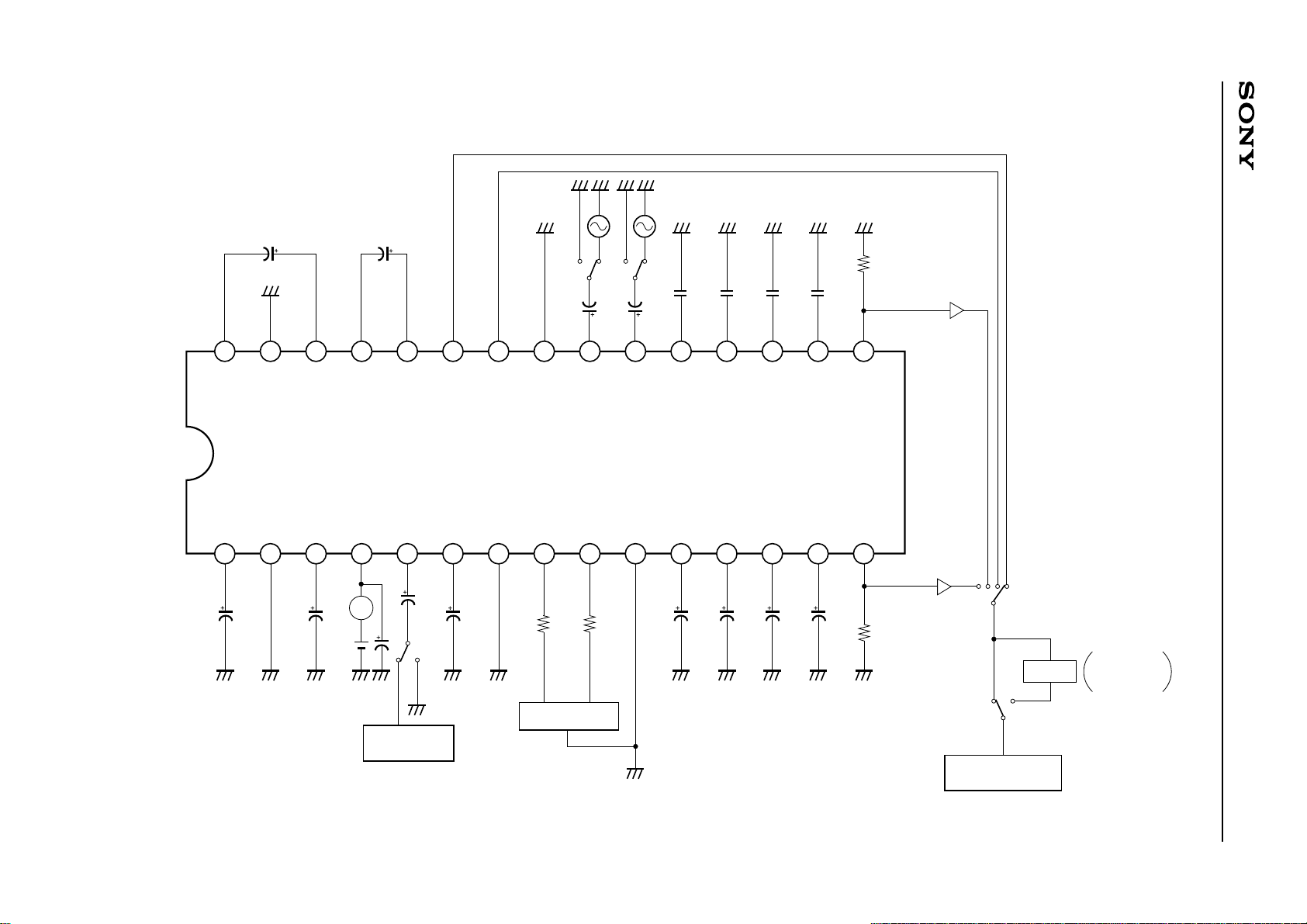
Electrical Characteristics Measurement Circuit
C17
1µ
30 29 28 27 26 25 24 23 22 21 20 19 18 17 16
C16
1µ
SW22
V2
C15
4.7µ
SW21
V1
C14
4.7µ
C13
0.01µ
C12
0.01µ
C11
4700p
C10
4700p
R4
10k
X1
SC OUT
NC
SC IN
MC OUT
MC IN
TV OUT-L
NC
TV OUT-R
AUX-L
AUX-R
CL-R
CL-L
CH-R
CH-L
LS OUT-L
– 10 –
SUBI
GND
REFL
Vcc
MPX IN
CUBI
NC
SDA
SCL
DGND
BAL
TRE
BASS
VOL
LS OUT-R
1 2 3 4 5 6 7 8 9 10 11 12 13 14 15
X1
C1
1µ
C2
1µ
Vcc
9V
A
C3
47µ
SIGNAL
GENERATOR
C4
1µ
SW20
C5
1µ
R1
220R2220
2
C BUS DATA
I
C6
0.1µC70.1µC80.1µC90.1µ
DGND
R3
10k
MEASURES
(AC VOLTMETER)
SW
SW
FILTER
1kHz BPF
15kHz LPF
30kHz LPF
CXA2013M
Page 11
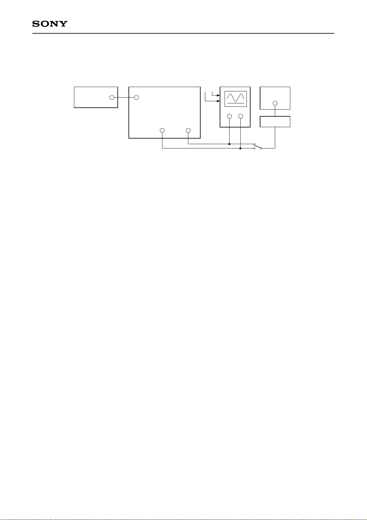
Adjustment method
Separation adjustment
CXA2013M
EIAJ sound multiplexing encoder OscilloscopeApplication circuit
MPX IN
TV OUT-L
TV OUT-R
LR
CH1
CH2
AC V oltmeter
15kHz LPF
Switch
Fig. 1
Procedure
1) Connect components as shown in Fig.1. (TEST = 0)
2) Set the encoder to MONO mode, and input 110mVrms (1kHz 100% modulation) to MPX IN (Pin 5).
3) Set the encoder to stereo mode, and input only left channel signal (1kHz 100% modulation) to MPX IN
(Pin 5).
4) Monitor the oscilloscope and AC voltmeter and adjust ATT so that the R-ch is at a minimum.
(Separation standard: more than 35dB)
– 11 –
Page 12
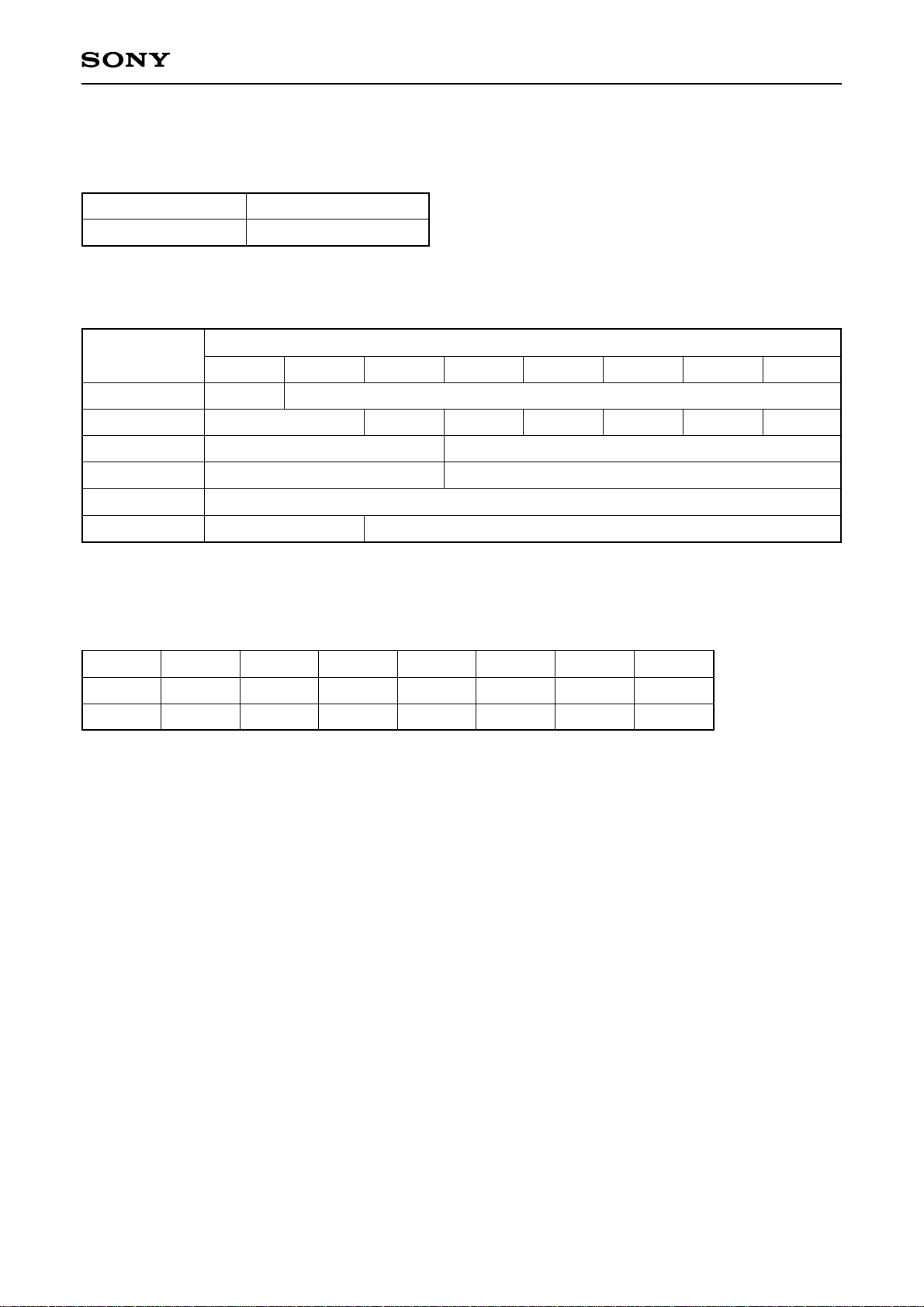
Register Specification
Slave address
CXA2013M
SLAVE RECEIVER
84H
Register table
SUB ADDRESS
MSB LSB
∗∗∗∗0000
∗∗∗∗0001
∗∗∗∗0010
∗∗∗∗0011
∗∗∗∗0100
∗∗∗∗0101
Status resigter
SLA VE TRANSMITTER
85H
DA TA
BIT7 BIT6 BIT5 BIT4 BIT3 BIT2 BIT1 BIT0
TEST
∗
∗
∗
∗
∗
∗
EXT
∗
∗
FOMO S1 S0
ATT (7)
MUTE TV MUTE LS
BASS (5)
TREBLE (5)
VOL (8)
∗
∗
BAL (6)
∗: Don't care
STA1
BIT7
PON
STA2
BIT6
ST
STA3
BIT5
BIL
STA4
BIT4
—
STA5
BIT3
—
STA6
BIT2
—
STA7
BIT1
—
STA8
BIT0
—
Note) When the IC is powered on, the registers "MUTE TV", "MUTE LS" and "VOL" are set to "0".
– 12 –
Page 13
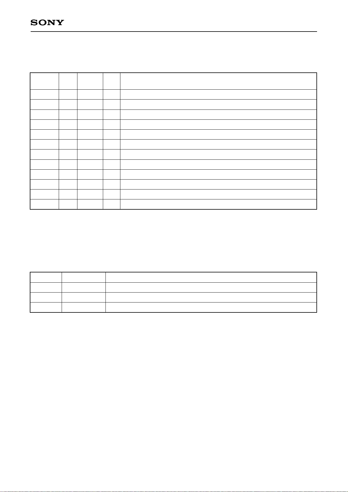
Description of registers
Control registers
CXA2013M
Register
Number
of bits
TEST
ATT
EXT
FOMO
S1
S0
MUTE TV
MUTE LS
BASS
TREBLE
VOL
BAL
∗
Classification U: User control
Classi-
∗
fication
1
7
1
1
1
1
1
1
5
5
8
6
T
A
U
U
U
U
U
U
U
U
U
U
A: Adjustment
T: Test (when IC manufactured)
Standard
setting
0
34
0
0
0
0
1
1
10
10
FF
20
Contents
DAC test mode for VCA, checking Cue BPF mode. 1: TEST
Adjustment of stereo separation
Selection of TV mode or external input mode for LSOUT output
Selection of forced MONO mode ON/OFF 1:
1: External
Forced MONO
Selection of TV OUT, LS OUT output signal
Selection of TV OUT, LS OUT output signal
Selection of TV OUT mute ON/OFF 0: Mute ON, 1: Mute OFF
Selection of LS OUT mute ON/OFF 0: Mute ON, 1: Mute OFF
LS OUT output bass control
LS OUT output treble control
LS OUT output signal level control
LS OUT-L, R output signal level (balance) control
Status Registers
Register
Number of bits Contens
PON
ST
BIL
1
1
1
POWER ON RESET detection 1: RESET
Stereo detection of the MPXIN input signal 1: Stereo
Bilingual detection of the MPXIN input signal 1: Bilingual
– 13 –
Page 14

CXA2013M
Description of Control Registers
TEST (1) : DAC test mode for VCA and checking Cue BPF mode.
Use only for the electrical characteristics inspection process of IC.
0 = Normal mode
1 = Test mode, the Cue signal component through Cue BPF to TV OUT-L.
Output DAC voltage for VCA to TV OUT -R.
ATT (7) : Perfor m the separation adjustment by varying the signal level input to MPX IN (Pin 5).
Va riable range of the input signal: Normal input level ±3.0dB
0 = Level Min.
34 = Center
7F = Level Max.
EXT (1) : Select TV mode or external input mode for LS OUT output
0 = TV mode
1 = External input mode
FOMO (1) : Select ON/OFF forced MONO mode
0 = Forced MONO OFF
1 = Forced MONO ON
S1 (1) : Select output signal for TV OUT, LS OUT
S0 (1) : Select output signal for TV OUT, LS OUT
MUTE TV (1) : Mute TV OUT output
0 = Mute ON
1 = Mute OFF
MUTE LS (1) : Mute LS OUT output
0 = Mute ON
1 = Mute OFF
BASS (5) : LS OUT output bass control
0 = Bass Min.
10 = Bass Center (0dB)
1F = Bass Max.
TREBLE (5) : LS OUT output treble contorl
0 = Treble Min.
10 = Treble Center (0dB)
1F = Treble Max.
VOL (8) : LS OUT output signal level control
0 = Volume Min. (–90dB Typ.)
FF = Volume Max. (0dB)
BAL (6) : LS OUT-L, R output signal level (balance) control
0 = Lch Min., Rch Max.
20 = Center (Lch 0dB, Rch 0dB)
3F = Lch Max., Rch Min.
– 14 –
Page 15
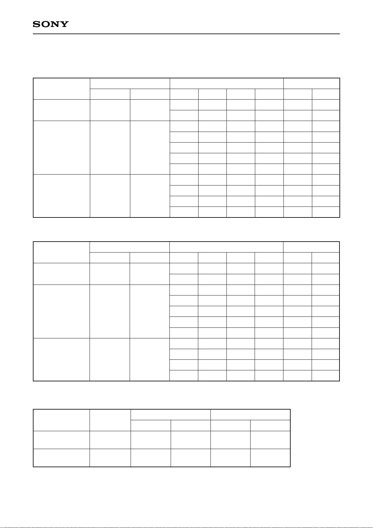
Description of Mode Control
TV OUT output mode control table (TEST = 0 normal mode)
CXA2013M
Input signal
Mode detection Mode control TV OUT output
MONO
Stereo
Bilingual
ST BIL FOMO S1 S0
∗
∗
00
∗
∗
1
1
0
0
0
0
∗
∗
0
1
∗
∗
∗
∗
∗
0
0
1
∗
0
0
1
MUTE TV
∗
∗
∗
∗
0
1
0
∗
0
1
0
LS OUT output mode control table (TEST = 0 normal mode, EXT = 0 TV mode)
Mode detection Mode control LS OUT output
Input signal
ST BIL FOMO S1 S0
MUTE LS
LR
0
1
0
1
1
1
1
0
1
1
1
MUTE
MAIN
MUTE
L + R
L
L
L
MUTE
MAIN
SUB
MAIN
MUTE
MAIN
MUTE
L + R
R
R
R
MUTE
MAIN
SUB
SUB
∗: Don't care
LR
MONO
Stereo
Bilingual
∗
00
∗
∗
1
1
0
0
0
0
∗
∗
0
1
∗
∗
∗
∗
∗
∗
0
0
1
∗
0
0
1
TV OUT/LS OUT output mode control table (TEST = 0 normal mode)
TV OUT
EXT
TV mode
L
0
TV mode
Lch
RLR
TV mode
Rch
TV mode
Lch
∗
∗
∗
∗
0
1
0
∗
0
1
0
LS OUT
0
1
0
1
1
1
1
0
1
1
1
TV mode
Rch
MUTE
MAIN
MUTE
L + R
L
L
L
MUTE
MAIN
SUB
MAIN
MUTE
MAIN
MUTE
L + R
R
R
R
MUTE
MAIN
SUB
SUB
∗: Don't care
External mode
1
TV mode
Lch
TV mode
Rch
EXT
Lch
EXT
Rch
– 15 –
Page 16

CXA2013M
Description of Operation
The sound mutiplexing signal input from Pin 5 is passed through IN AMP and is applied to the Cue BPF, Sub
BPF, and Main de-emphasis circuit.
1. Discrimination circuits
Cue BPF passes only the Cue signal component from the multiplex signal. In the AM demodulator, the
signal (AM wave) is AM detected and one of two sine waves is generated, either a 922.5Hz signal for
bilingual broadcasts or a 982.5Hz signal for stereo broadcasts.
In the 952Hz BPF, the 3.5fH carrier component is eliminated from the Cue signal after AM wave detection.
The Cue signal, from which the carrier component has been eliminated, is waveform shaped by COMP, with
the resulting 922.5Hz or 982.5Hz pulse being applied to the Logic section.
In the 3.5fH VCO, a 3.5fH pulse locked onto the Cue signal carrier (3.5fH) is created and sent to the Logic
section.
In the Logic section, the broadcast mode is identified using the countdown method. Depending on this
result as well as the presence of a SUB signal from SUB detector and the MUTE ON/OFF, MODE
switching, and FOMO ON/OFF instructions from CONT, the output switching control signal is created. This
signal is used to control the output condition of OUTPUT SW and MAIN OUT.
2. Main circuits
In MAIN DEEM, de-emphasis is applied to the Main signal component and the Sub and Cue components
are removed.
After passing through the MAIN DEEM, the Main signal is applied to MATRIX, OUTPUT AMP, and
MAINOUT.
3. Sub circuits
In SUB BPF, only the SUB signal component out of multiplex signals is passed through. In the 4.5fH trap,
the digital facsimile signal component is removed.
In FM Demod, the SUB signal is FM demodulated.
In SUB DEEM, the FM demodulated Sub signal is de-emphasized and the carrier component is removed.
After passing through SUB DEEM, the Sub signal is applied to MATRIX and OUTPUT AMP.
4. MATRIX and output circuits
In MATRIX, the L and R signals are created by adding and subtracting the Main signal from MAIN DEEM
and the Sub signal from SUB DEEM in stereo broadcast.
In OUTPUT AMP and OUTPUT SW, the output signal is switched under the control of Logic.
In addition, MAIN OUT always outputs the MAIN signal component, regardless of the broadcast mode.
5. TONE circuit
Control BASS and TREBLE. Bass and TREBLE characteristics are decided by each CL and CH external
capacitance.
6. BALANCE, VOLUME curcuit
Control BALANCE and VOLUME. BALANCE has 64steps and VOLUME has 256 steps.
7. DAC
DAC is the circuit that control BASS, TREBLE, VOLUME and BALANCE.
Internal impedance is approximately 20kΩ (approximately 5kΩ for VOLUME).
Connect the external capacitance for LPF to each pins.
– 16 –
Page 17
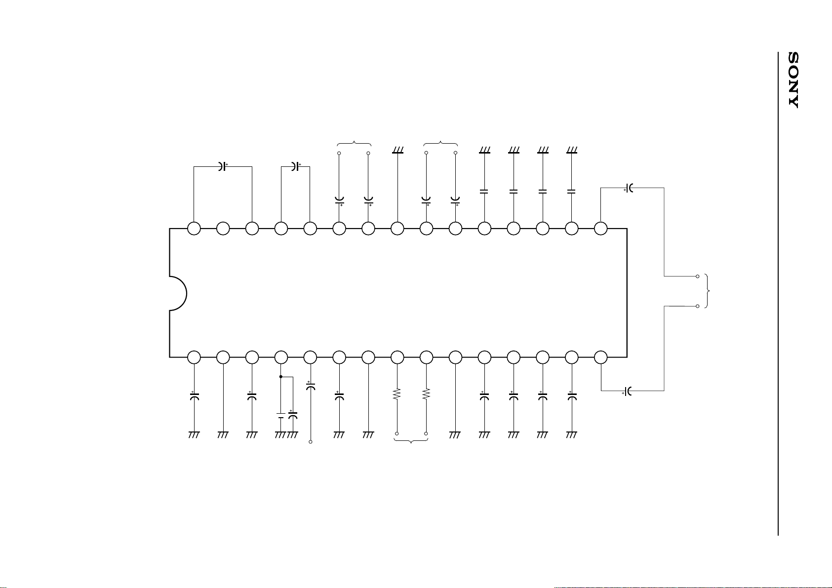
Application Circuit
TVOUT output
Vcc
9V
C20
1µ
MC OUT
Vcc
C3
100µ
MC IN
MPX IN
C4
10µ
C19
C18
10µ
10µ
2425 22 21
TV OUT-L
TV OUT-R
CUBI
NC
C5
10µ
C21
1µ
30 29 28 27 26 23 20 19 18 17 16
NC
SC OUT
SC IN
– 17 –
SUBI
GND
REFL
1 2 3 4 5 6 7 8 11 12 13 14 15
C1
10µ
C2
10µ
External input
NC
AUX-L
SDA
SCL
R1
220R2220
C17
10µ
AUX-R
DGND
109
C15
C14
0.1µ
C16
10µ
CL-R
BAL
0.1µ
CL-L
TRE
C6
4.7µC74.7µC84.7µC94.7µ
C13
4700p
CH-R
BASS
C12
4700p
CH-L
VOL
C11
10µ
LS OUT-L
LSOUT
output
LS OUT-R
C10
10µ
Composite
baseband
signal input
Application circuits shown are typical examples illustrating the operation of the devices. Sony cannot assume responsibility for
any problems arising out of the use of these circuits or for any infringement of third party patent and other right due to same.
µ-com
DGND
CXA2013M
Page 18
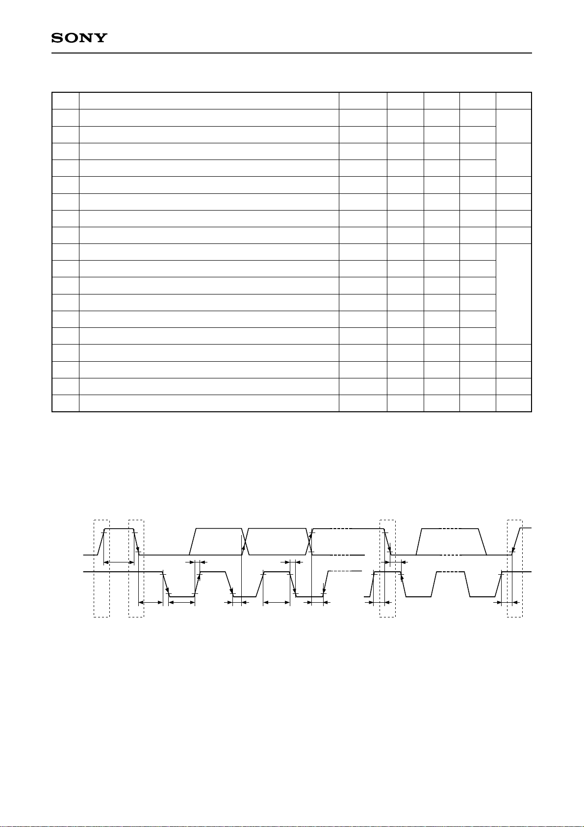
I2C Bus Block Items (SDA, SCL)
CXA2013M
No.
1
High level input voltage
2
Low level input voltage
3
High level input current
4
Low level input current
5
Low level output voltage SDA (Pin 8) during 3mA inflow
6
Maximum inflow current
7
Input capacitance
8
Maximum clock frequency
9
Minimum waiting time for data change
10
Minimum waiting time for start of data transfer
11
Low level clock pulse width
12
High level clock pulse width
13
Minimum waiting time for start preparation
14
Minimum data hold time
15
Minimum data preparation time
16
Rise time
17
Fall time
18
Minimum waiting time for stop preparation
Item
Symbol
VIH
VIL
IIH
IIL
VOL
IOL
CI
fSCL
tBUF
tHD:STA
tLOW
tHIGH
tSU:STA
tHD:DAT
tSU:DAT
tR
tF
tSU:STO
Min.
3.0
0
—
—
0
3
—
0
4.7
4.0
4.7
4.0
4.7
0
250
—
—
4.7
Typ.
—
—
—
—
—
—
—
—
—
—
—
—
—
—
—
—
—
—
Max.
5.0
1.5
10
10
0.4
—
10
100
—
—
—
—
—
—
—
1
300
—
Unit
V
µA
V
mA
pF
kHz
µs
ns
µs
ns
µs
I2C bus load conditions: Pull-up resistor 4kΩ (Connect to +5V)
Load capacitor 200pF (Connect to GND)
I2C Bus Control Signal
SDA
BUF
SCL
t
P
t
S
HD
:STA
t
R
LOW
t
tHD:DAT
t
t
HIGH
F
SU
:DAT
t
Sr
tHD:STA
t
SU
:STA
t
SU
:STO
P
– 18 –
Page 19

CXA2013M
I2C Bus Signal
There are I2C signals, SDA (Serial DATA) and SCL (Serial CLOCK) signals. SDA is a bidirectional signal.
• Accordingly there are 3 values outputs, H, L, and Hi-Z.
H L Hi-Z L
• I2C transfer begins with Start Condition and ends with STOP condition.
Start Condition S Stop Condition P
SDA
SCL
– 19 –
Page 20
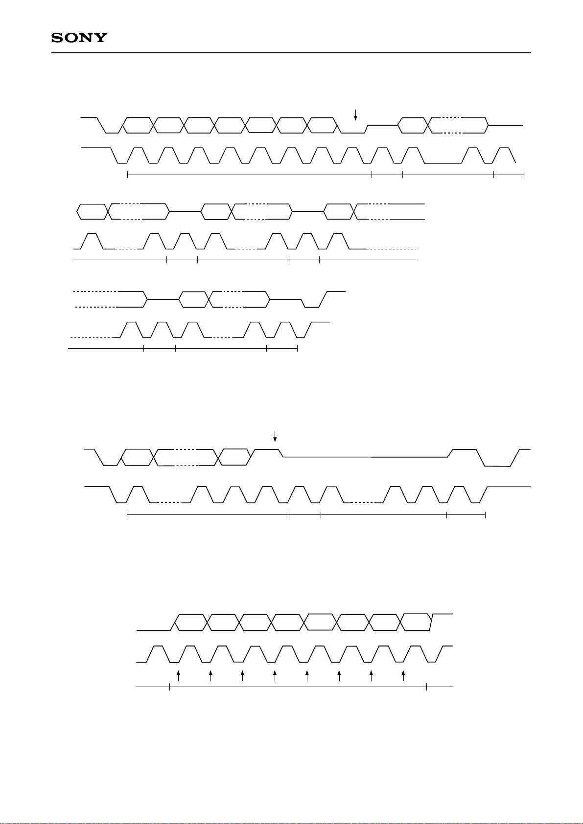
• I2C data write (Write from I2C controller to the IC)
MSB
SDA
L during Write
CXA2013M
MSB LSB
Hi-Z Hi-Z
SCL
S
189189
DATA (n) DATA (n + 1)ACK
1234567891 89
Address
LSBMSB
Hi-Z Hi-Z
Hi-Z Hi-Z
891 89
ACKACKDATA DATA
• I2C data read (Read from the IC to I2C controller)
H during Read
ACK DATA (n + 2)
∗
P
ACK Sub Address ACK
Data can be transferred in 8-bit units to be
set as required.
Sub address is incremented automatically.
SDA
SCL
167891 89
S
Address
• Read timing
MSB LSB
IC output SDA
SCL
Read timing
∗
Data Read is performed during SCL rise.
ACK ACK
123456789 9
Hi-Z
7
P
ACK DATA ACK
DATA
– 20 –
Page 21
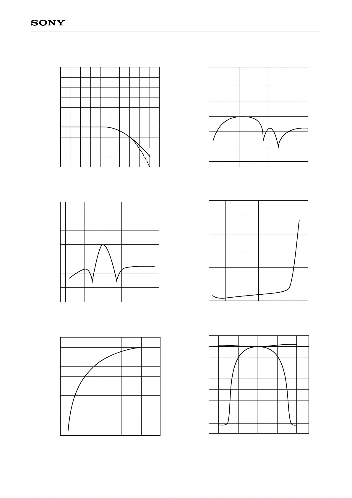
Example of Representative Characteristics
CXA2013M
0
Output level [dB]
–5
–10
–15
De-emphasis characteristics
Main
100 1k 10k
Frequency [Hz]
Cue BPF frequency characteristics
Sub
Output level [dB]
–20
–40
–60
SUB BPF frequency characteristics
0
10
20 30 40 50 60 70 80 10090
Frequency [kHz]
MAIN distortion characteristics
3
0
–20
Attenuation level [dB]
–40
–60
0
–10
–20
–30
–40
–50
LS OUT-L, R [dB]
–60
–70
–80
3.5f
H
–40k
3.5f
–20k
H
H
3.5f
Frequency [Hz]
3.5f
+20k
VOL CONTROL characteristics
40 80 C0 FF
BUS data [VOL]
2
Distortion [%]
1
100
H
3.5f
+40k
H
200 300 400 500
MAIN modulation factor [%]
BALANCE CONTROL characteristics
0
–10
–20
–30
–40
LS OUT-L, R [dB]
–50
–60
–70
–80
OUT R
0
10 20 30 3F
BUS data [BALANCE]
OUT L
– 21 –
Page 22
20
10
0
LS OUT -L, R [dB]
–10
CXA2013M
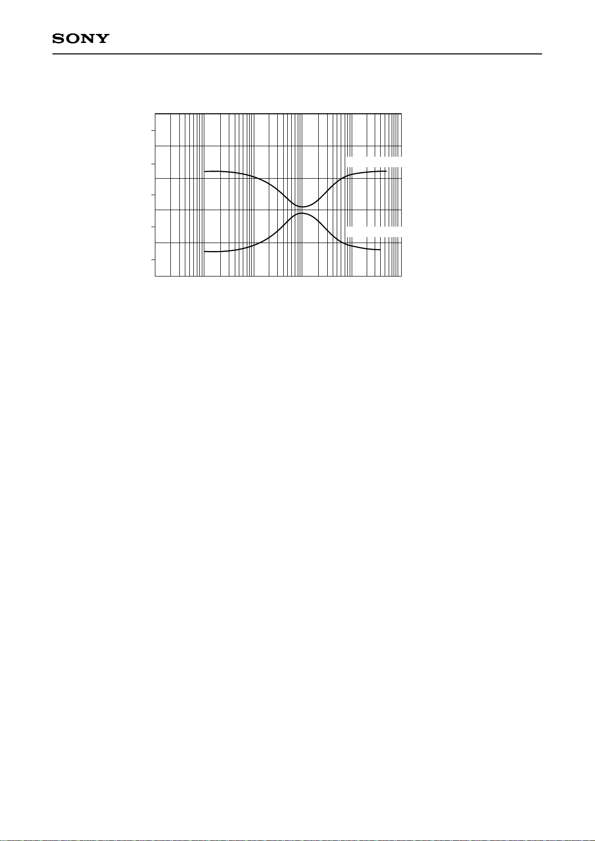
TONE characteristics
BASS-TREBLE MAX.
BASS-TREBLE MIN.
–20
100 1k 10k
Frequency [Hz]
– 22 –
Page 23
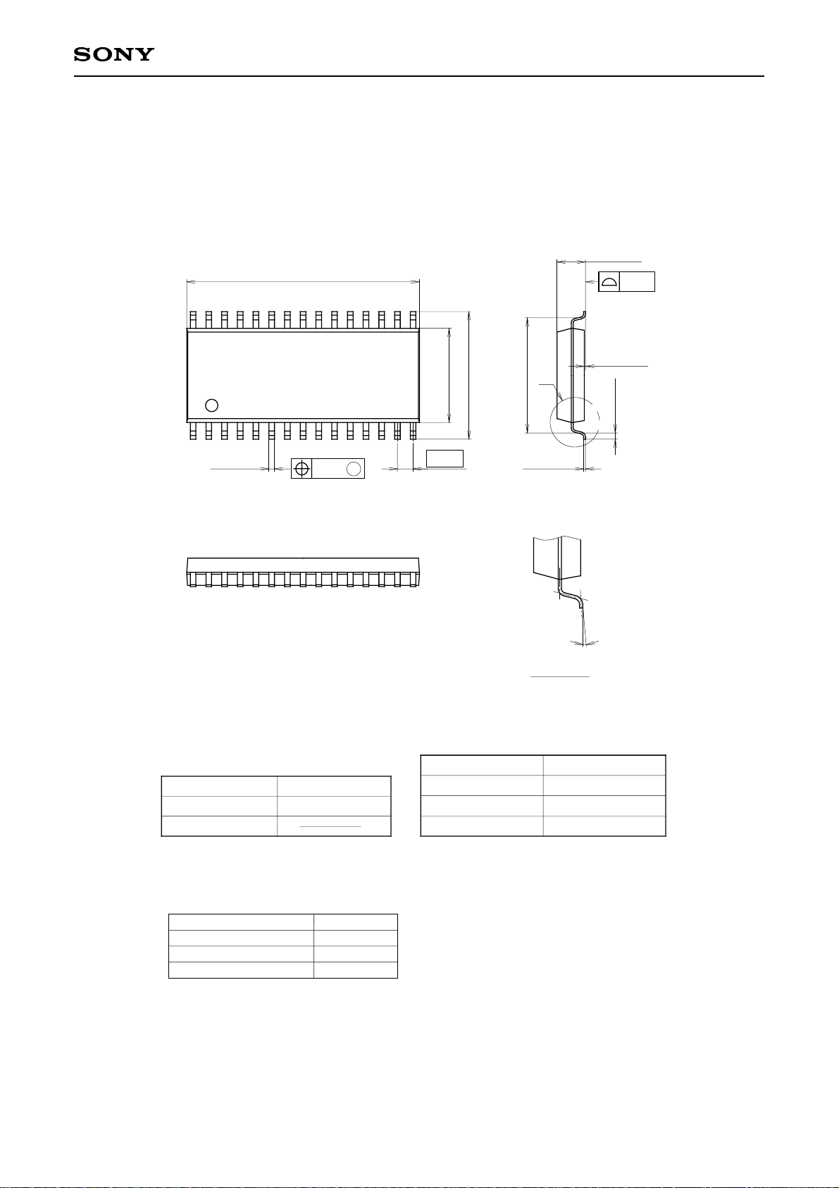
Packag e Outline Unit: mm
30
1
0.45 ± 0.1
+ 0.4
18.8 – 0.1
30PIN SOP (PLASTIC)
16
+ 0.3
– 0.1
7.6
15
0.2
M
1.27
10.3 ± 0.4
A
(9.3)
+ 0.1
0.2 – 0.05
+ 0.4
2.3 – 0.15
+ 0.2
0.1 – 0.05
0.5 ± 0.2
CXA2013M
0.1
SONY CODE
EIAJ CODE
JEDEC CODE
LEAD PLATING SPECIFICATIONS
ITEM
LEAD MATERIAL COPPER ALLOY
SOLDER COMPOSITION Sn-Bi Bi:1-4wt%
PLA TING THICKNESS 5-18µm
SOP-30P-L03
SOP030-P-0375
SPEC.
0˚ to 10˚
DETAIL A
PACKAGE STRUCTURE
PACKAGE MATERIAL
LEAD TREA TMENT
LEAD MATERIAL
PACKAGE MASS
EPOXY RESIN
SOLDER PLATING
COPPER ALLOY
0.7g
– 23 –
Sony Corporation
 Loading...