

Page 1
Analog signal processor IC
For the availability of this product, please contact the sales office.
Description
The CXA2027Q is an analog signal processor for
CCD linear image sensor output signal. This device
is suitable for 3 lines of full-color CCD linear image
sensor (ILX516K/ILX518K/ILX520K: 3648 pixels ×
3 lines/5363 pixels × 3 lines/7078 pixels × 3 lines).
This device has a built-in sample-and-hold, clamp,
multiplex, gain control amplifier circuits and can be
connected directly with external AD converters.
(Sony’s CXD2311AR, CXD1175AM or CXA1977R
are recommended as AD converters.)
Features
• Sample-and-hold circuit
• Pixel-clamp and line-clamp circuit
• Multiplex circuit
• ADC driver circuit
• Gain control amplifier circuit
• Offset control circuit
• Clock frequency: 1.5 to 6MHz (after multiplex)
Applications
Color image scanner
CXA2027Q
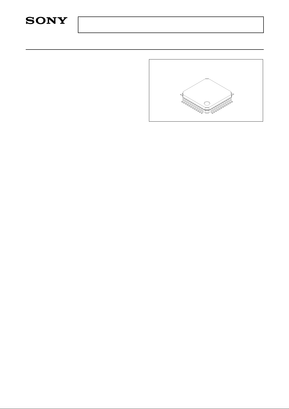
48 pin QFP (Plastic)
Absolute Maximum Ratings
• Supply voltage VCC –0.3 to 7 V
• Input voltage VI –0.3 to VCC + 0.3 V
• Output voltage VO –0.3 to VCC + 0.3 V
• Storage temperature Tstg –55 to +150 °C
• Allowable power dissipation
PD 640 mW
Operating Conditions (Typ. in parentheses)
• Supply voltage VCC 4.75 to 5.25 (5.0) V
• Digital input voltage High VIH 3.5 to VCC (VCC)V
•Digital input voltage Low VIL 0 to 0.8 (0) V
• Operating temperature Topr 0 to +70 °C
Structure
Bipolar silicon monolithic IC
Sony reserves the right to change products and specifications without prior notice. This information does not convey any license by
any implication or otherwise under any patents or other right. Application circuits shown, if any, are typical examples illustrating the
operation of the devices. Sony cannot assume responsibility for any problems arising out of the use of these circuits.
– 1 –
E95210A78
Page 2
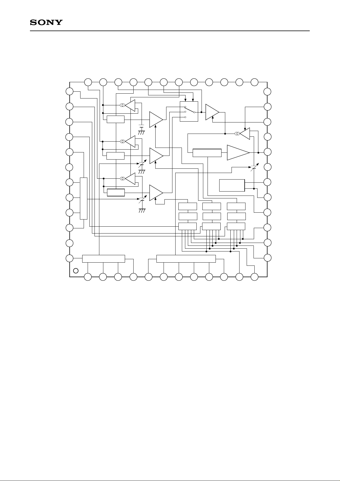
Block Diagram and Pin Configuration
CXA2027Q
B-IN
LPR
LPG
LPB
D4-0
VCCA
D4-1
D4-2
D4-3
D4-4
37
38
39
40
41
42
43
44
45
46
36
D/A
G-IN
35
R-IN
S/H
S/H
S/H
34
BUF
33
SH
32
MPX2
GCA
GCA
GCA
MPX1
31
TD3
CLP
30
29
DC shift
LOG
D/A
LATCH LATCH
TD1
TD2
27
28
GCA
Driver
VREF
LOG
D/A D/A
LOG
LATCH
26
TD5
25
TD6
24
23
22
21
20
19
18
17
16
15
TD4
LCLP
GC
VCCP
SIGOUT
GND
VRT
VRB
CLPC
LD4
VCCD
D5-0
47
48
D5-1
D/A
2
D5-2
3
D5-3
4
D5-4
5
D6-0
6
D6-1
7
D/A
D6-2
8
D6-3
9
D6-4
10
D6-5
11
LD0
14
LD3
13
LD2
121
LD1
– 2 –
Page 3
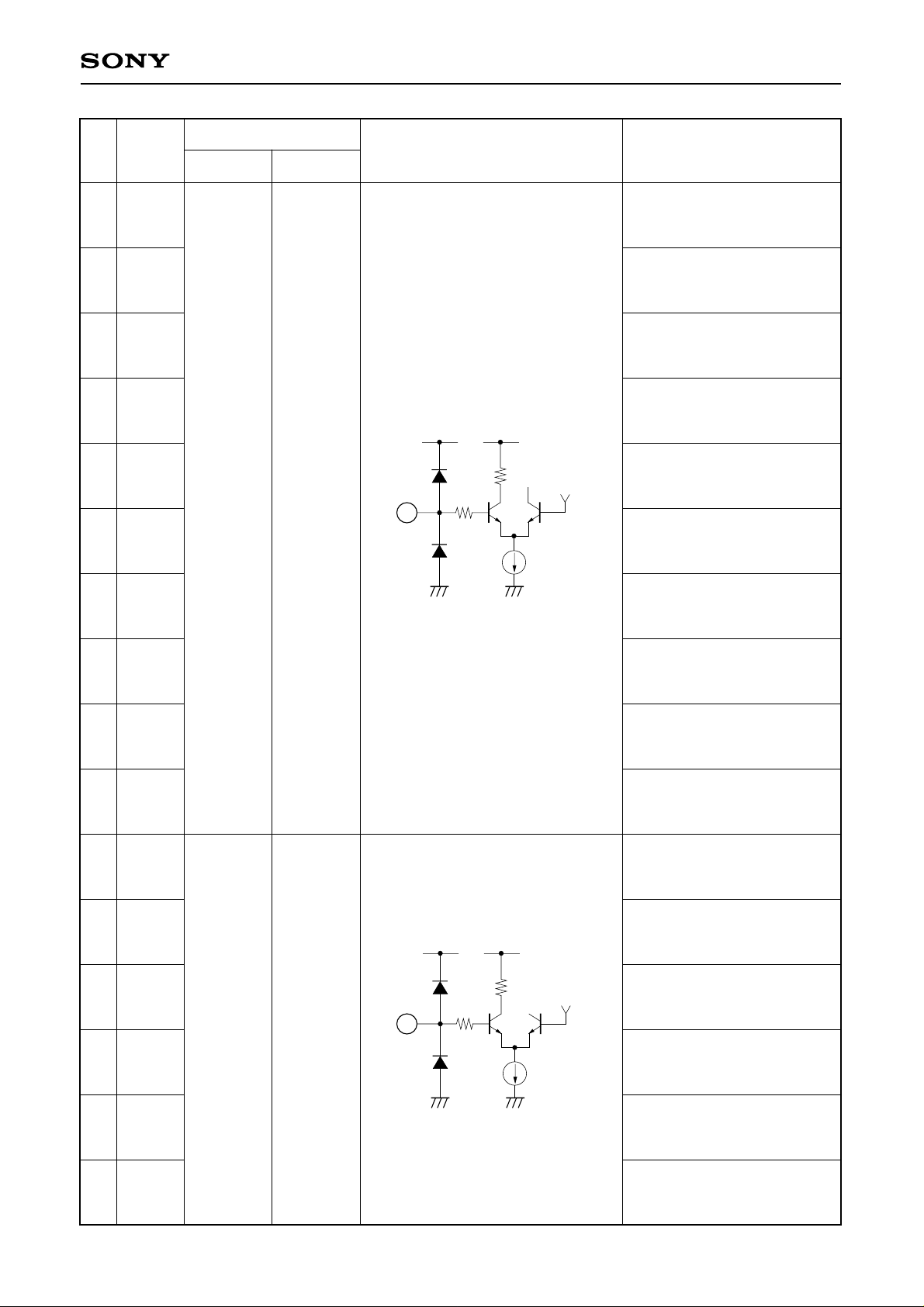
Pin Description
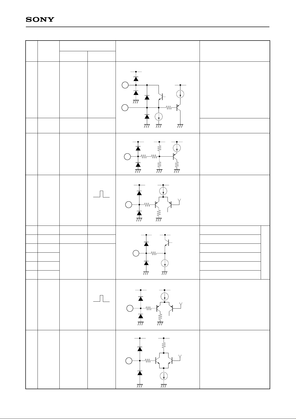
CXA2027Q
Pin
No.
48
1
2
3
4
41
43
Symbol
(I/O)
D5-0 (I)
D5-1 (I)
D5-2 (I)
D5-3 (I)
D5-4 (I)
D4-0 (I)
D4-1 (I)
Typical pin voltage
DC AC
Lo: 0 to 0.8V
Hi: 3.5 to 5V
Equivalent circuit Description
5-bit data input pin 1 for
G channel pixel clamp
voltage adjustment (LSB)
5-bit data input pin 2 for
G channel pixel clamp
voltage adjustment
5-bit data input pin 3 for
G channel pixel clamp
voltage adjustment
5-bit data input pin 4 for
G channel pixel clamp
VCCD VCCD
voltage adjustment
5-bit data input pin 5 for
G channel pixel clamp
voltage adjustment (MSB)
5-bit data input pin 1 for
48
129
1.5k
1.8V
B channel pixel clamp
100µ
voltage adjustment (LSB)
5-bit data input pin 2 for
B channel pixel clamp
voltage adjustment
44
45
46
5
6
7
8
D4-2 (I)
D4-3 (I)
D4-4 (I)
D6-0 (I)
D6-1 (I)
D6-2 (I)
D6-3 (I)
Lo: 0 to 0.8V
Hi: 3.5 to 5V
VCCD VCCD
5
129
1k
100µ
1.8V
5-bit data input pin 3 for
B channel pixel clamp
voltage adjustment
5-bit data input pin 4 for
B channel pixel clamp
voltage adjustment
5-bit data input pin 5 for
B channel pixel clamp
voltage adjustment (MSB)
6-bit data input pin 1 for
SIGOUT output line clamp
voltage adjustment (LSB)
6-bit data input pin 2 for
SIGOUT output line clamp
voltage adjustment
6-bit data input pin 3 for
SIGOUT output line clamp
voltage adjustment
6-bit data input pin 4 for
SIGOUT output line clamp
voltage adjustment
9
10
D6-4 (I)
D6-5 (I)
6-bit data input pin 5 for
SIGOUT output line clamp
voltage adjustment
6-bit data input pin 6 for
SIGOUT output line clamp
voltage adjustment (MSB)
– 3 –
Page 4
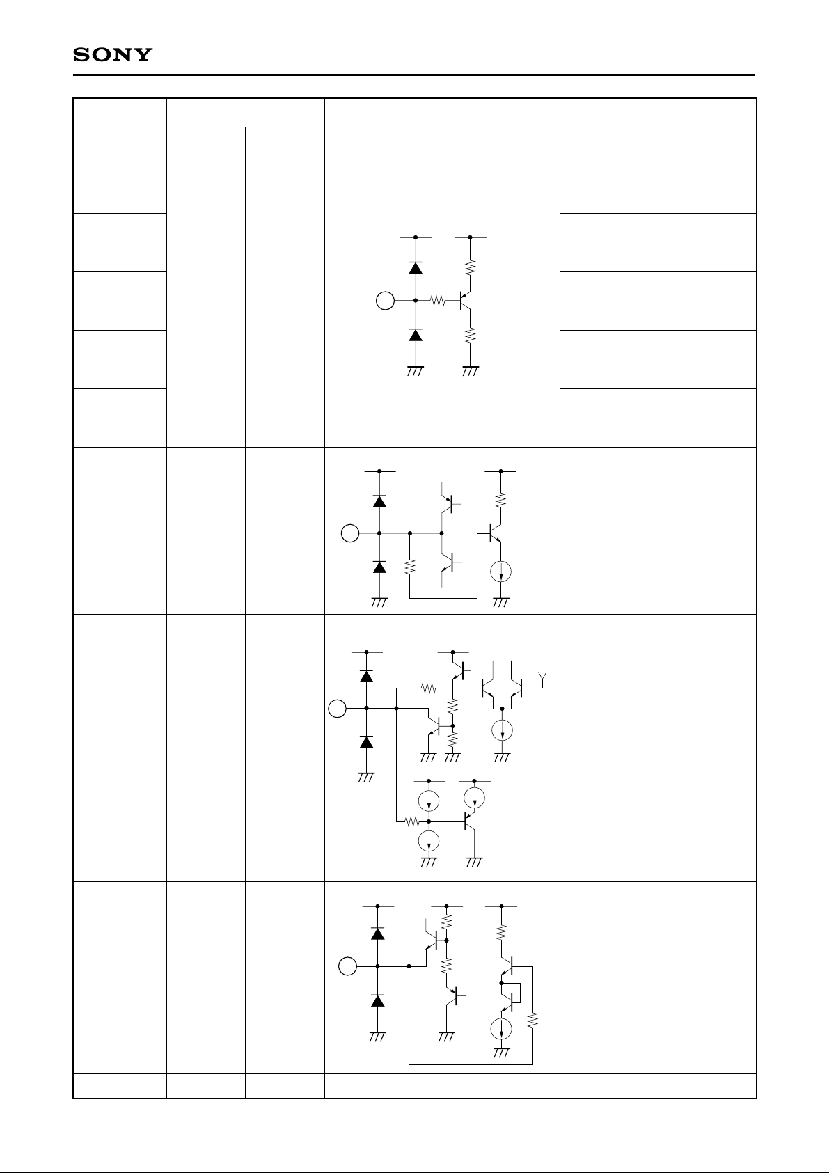
CXA2027Q
Pin
No.
11
12
13
14
15
16
Symbol
(I/O)
LD0 (I)
LD1 (I)
LD2 (I)
LD3 (I)
LD4 (I)
CLPC
Typical pin voltage
DC AC
Lo:
0 to 0.8V
Hi:
3.5 to 5V
Approx.
3.1V
16
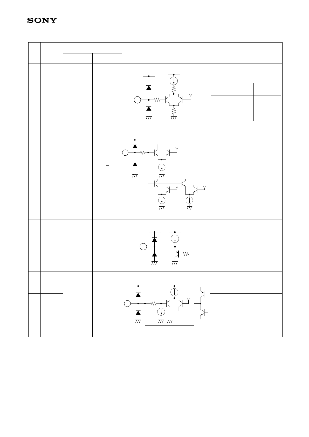
Equivalent circuit Description
5-bit data input pin 1 for
pre-stage GCA gain
adjustment (LSB)
VCCD VCCD
5-bit data input pin 2 for
pre-stage GCA gain
20k
adjustment
5-bit data input pin 3 for
11
129
1.5k
pre-stage GCA gain
adjustment
5-bit data input pin 4 for
pre-stage GCA gain
adjustment
5-bit data input pin 5 for
pre-stage GCA gain
adjustment (MSB)
VCCA
VCCA
1.5k
Additional capacitance pin
for line clamp.
Add 0.47µF between this
129
6.7µ
pin and GND.
17
18
VRB (O)
VRT (O)
2.0V
4.0V
17
18
VCCA
VCCA
1k
6k
VCCA
VCCA
100µ
75µ
187.5
750
3k
2k
VCCA
100µ
100µ
VCCAVCCA
100µ
2k
2.0V
Output pin for AD converter
reference voltage VRB
Output pin for AD converter
reference voltage VRT
4k
19
GND
0V
GND pin
– 4 –
Page 5
CXA2027Q
Pin
No.
20
21
22
23
Symbol
(I/O)
SIGOUT
(O)
VCCP
GC (I)
LCLP (I)
Typical pin voltage
DC AC
2.0V
+MAX1.8V
(2.0 to 3.8V)
5V
0 to 5V
Lo: 0 to 0.8V
Hi: 3.5 to 5V
Lo:
clamp OFF
Hi:
clamp ON
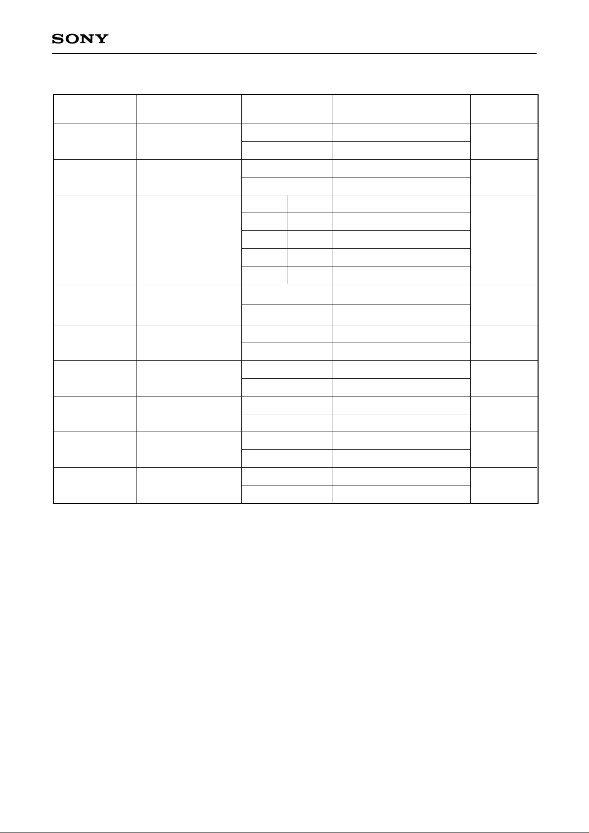
Equivalent circuit Description
VCCA
21
20
VCCA VCCA
129
22
VCCA VCCA
23
129
4k
2mA
20k
30k
2k
1k
100µ
VCCA
VCCA
100µ
1.5k
1.5V
100µ
Signal output pin
(to AD converter)
Power supply pin
(for signal output system)
Voltage input pin for poststage GCA gain adjustment
(Can be open; in that case
outputs 3V)
Line clamp pulse input pin
(Apply high level during the
optical black period of CCD
output)
24
25
26
27
28
29
30
31
TD4 (O)
TD6 (O)
TD5 (O)
TD1 (O)
TD2 (O)
TD3 (O)
CLP (I)
MPX1 (I)
1.7 to 3.6V
2.0 to 3.6V
1.7 to 3.6V
Lo: 0 to 0.8V
Hi: 3.5 to 5V
Lo:
clamp OFF
Hi:
clamp ON
Lo: 0 to 0.8V
Hi: 3.5 to 5V
VCCA VCCA
24
VCCA
129
30
VCCA VCCA
31
129
129
VCCA
1k
126µ
250µ
1.5k
100µ
1.5V
1.2V
DA4 analog output test pin
DA6 analog output test pin
DA5 analog output test pin
DA1 analog output test pin
DA2 analog output test pin
DA3 analog output test pin
Pixel clamp pulse input pin
(Apply high level during the
precharge period of CCD
output)
MPX channel switching
pulse input pin 1
(See high/low table under
Pin 32 in following section.)
(Use with open)
– 5 –
Page 6
CXA2027Q
Pin
No.
32
33
Symbol
(I/O)
MPX2 (I)
SH (I)
Typical pin voltage
DC AC
Lo: 0 to 0.8V
Hi: 3.5 to 5V
Lo: 0 to 0.8V
Hi: 3.5 to 5V
Lo: sample
mode
Hi: hold
mode
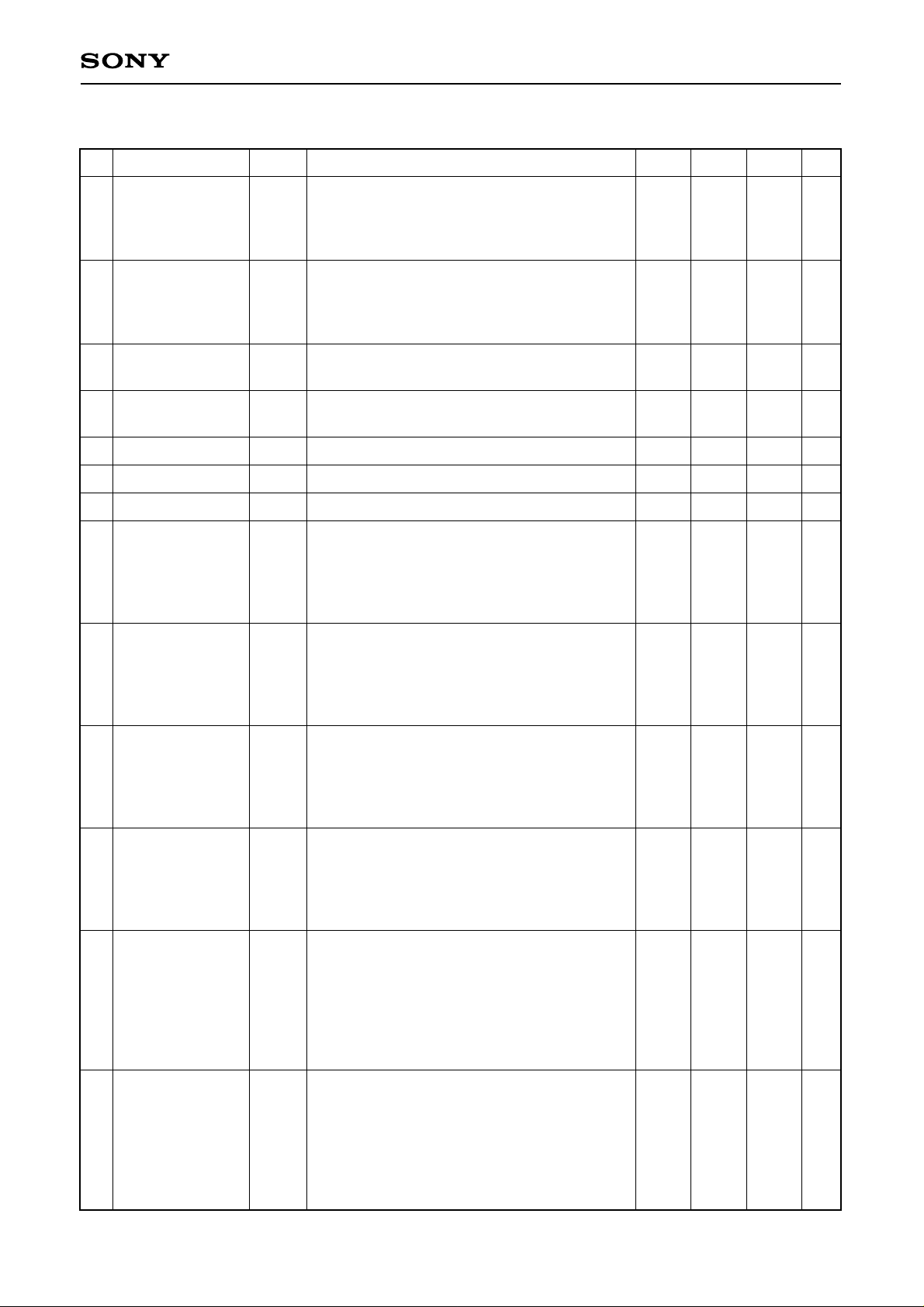
Equivalent circuit Description
VCCA
32
VCCA
33
129
VCCA
130µ
5k
2.4V
129
1.5k
1.5V
1m
MPX channel switching pulse
input pin 2.
Pin 31 Pin 32 Pin 20
MPX1 MPX2 SIGOUT
LL
LHG
HLB
HHB
R channel
channel
channel
channel
Sample-and-hold pulse input
pin.
(Apply low level during the
effective signal period (refer
1.5V
to Note 1) of CCD output)
1.5V
1m
1m
34
35
36
37
BUF (O)
R-IN (I)
G-IN (I)
B-IN (I)
2.4V
+MAX1.8V
(2.4 to 4.2V)
CCD
effective
signal level
MAX1.5Vp-p
(Note 1)
VCCA VCCA
34
VCCA VCCA
35
129
1µ
260µ
100µ
2k
3.7V
Output test pin after MPX
(use with open)
CCD signal R channel input
pin
CCD signal G channel input
pin
CCD signal B channel input
pin
– 6 –
Page 7

CXA2027Q
Pin
No.
38
39
40
42
47
Symbol
(I/O)
LPR (I)
LPG (I)
LPB (I)
VCCA
VCCD
Typical pin voltage
DC AC
Lo: 0 to 0.8V
data hold
Hi: 3.5 to 5V
data input
5V
5V
Equivalent circuit Description
Voltage input pin for setting
R channel pre-stage GCA
gain adjustment latch circuit
VCCD VCCD
to data input mode (high) or
hold mode (low).
1.5k
Voltage input pin for setting
G channel pre-stage GCA
38
129
28k
gain adjustment latch circuit
to data input mode (high) or
hold mode (low).
Voltage input pin for setting
B channel pre-stage GCA
gain adjustment latch circuit
to data input mode (high) or
hold mode (low).
Power supply pin
(for analog, general system)
Power supply pin
(for DA converter system)
Note 1: Effective signal levels are defined as follows for CCD output signals.
Reset level
CCD output signal
Precharge level
Effective signal level
Fig. 1
– 7 –
Page 8
Description of Data Input Pin Polarity
CXA2027Q
Pin name
(Pin No.)
CLP(30)
SH(33)
MPX1/MPX2
(31/32)
LPR/LPG/LPB
(38/39/40)
LD0 to LD4
(11/12/13/14/15)
D4-0 to D4-4
(41/43/44/45/46)
D5-0 to D5-4
(48/1/2/3/4)
D6-0 to D6-5
(5/6/7/8/9/10)
LCLP(23)
Function Input level Characteristics Others
Pixel clamp
Sample-and-hold
Channel switching for
R,G,B
Channel switching for
pre-stage GCA gain
data input
Pre-stage GCA gain
data
B-IN clamp voltage
adjustment
G-IN clamp voltage
adjustment
Output DC voltage
adjustment
Line clamp
MPX1
Low
Low
High
High
High
Low
High
Low
High
Low
11111
00000
11111
00000
11111
00000
111111
000000
High
Low
MPX2
Low
High
Low
High
Clamp ON
Clamp OFF
Hold mode
Sample mode
Output
R-ch
G-ch
B-ch
B-ch
Data input
Data hold
Maximum gain
Minimum gain
Maximum clamp voltage
Minimum clamp voltage
Maximum clamp voltage
Minimum clamp voltage
Maximum DC output voltage
Minimum DC output voltage
Clamp ON
Clamp OFF
LPR: for R-ch
LPG: for G-ch
LPB: for B-ch
LD0: LSB
LD4: MSB
D4-0: LSB
D4-4: MSB
D5-0: LSB
D5-4: MSB
D6-0: LSB
D6-5: MSB
– 8 –
Page 9
CXA2027Q
Electrical Characteristics (See Electrical Characteristics Measurement Circuit.) (VCC = 5V, Ta = 25°C)
No.
Current
1
consumption (1)
Current
2
consumption (2)
Digital input
3
voltage High
Digital input
4
voltage Low
5
VRB DC voltage
6
VRT DC voltage
7
VRT-VRB voltage
Pre-stage GCA
8
gain min.
Item Measurement conditions Min. Typ. Max. Unit
Symbol
Pre and Post-stage GCA gain = maximum
Icc1
SW11 to 15 = b, SW16 = a, SW22-1 = b,
SW22-2 = b, SW23 = a, SW31 to 32 = a,
44
60
78
mA
SW35-1 = a
Pre and Post-stage GCA gain = minimum
Icc2
SW11 to 15 = a, SW16 = a, SW22-1 = b,
SW22-2 = a, SW23 = a, SW31 to 32 = a,
54
73
94
mA
SW35-1 = a
Vih
Vil
Vrb
Vrt
Vtb
VRB-VRT equivalent impedance 300Ω
VRB-VRT equivalent impedance 300Ω
VRB-VRT equivalent impedance 300Ω
3.5
0
1.96
3.94
1.95
2.00
3.99
1.98
5
0.8
2.04
4.06
2.05
V
V
V
V
V
Minimum pre-stage GCA gain.
Input (0.4V) and output (V20) ratio.
Gfn
SW11 to 15 = a, SW16 = a, SW22-1 = a,
–1.67
–0.25
+1.11
dB
SW23 = a, SW35-1 = b, SW35-2 = a,
SW31, 32 = (a, a) or (a, b) or (b, b)
Pre-stage GCA
9
gain max.
Post-stage GCA
10
gain min.
Post-stage GCA
11
gain max.
12
Output signal
linearity 1
Output signal
13
linearity 2
Gfx
Grn
Grx
Lin1
Lin2
Maximum pre-stage GCA gain.
Input (0.4V) and output (V20) ratio.
SW11 to 15 = b, SW16 = a, SW22-1 = a,
SW23 = a, SW35-1 = b, SW35-2 = a,
SW31, 32 = (a, a) or (a, b) or (b, b)
Minimum post-stage GCA gain.
Input (0.4V) and output (V20) ratio.
SW11 to 15 = a, SW16 = a, SW22-1 = b,
SW22-2 = a, SW23 = a, SW35-1 = b,
SW35-2 = a, SW31 to 32 = a
Maximum post-stage GCA gain.
Input (0.4V) and output (V20) ratio.
SW11 to 15 = a, SW16 = a, SW22-1 = b,
SW22-2 = b, SW23 = a, SW35-1 = b,
SW35-2 = a, SW31 to 32 = a
Difference between output value 1/2 level
for input level Vx and output level for input
level 1/2 Vx.
Vx = 1.5V (SG35-2). See Note 2.
SW11 to 15 = a, SW16 = b, SW22-1 = a,
SW23 = b, SW31, 32 = (a, a) or (a, b) or (b, b),
SW35-1 = b, SW35-2 = b
Difference between output value 1/2 level
for input level Vx and output level for input
level 1/2 Vx.
Vx = 0.3V (SG35-2). See Note 2.
SW11 to 15 = a, SW16 = b, SW22-1 = a,
SW23 = b, SW31, 32 = (a, a) or (a, b) or (b, b),
SW35-1 = b, SW35-2 = b
11.77
–8.33
3.55
–5
–5
13.92
–6.92
5.24
16.03
–5.61
7.12
+5
+5
dB
dB
dB
%
%
– 9 –
Page 10
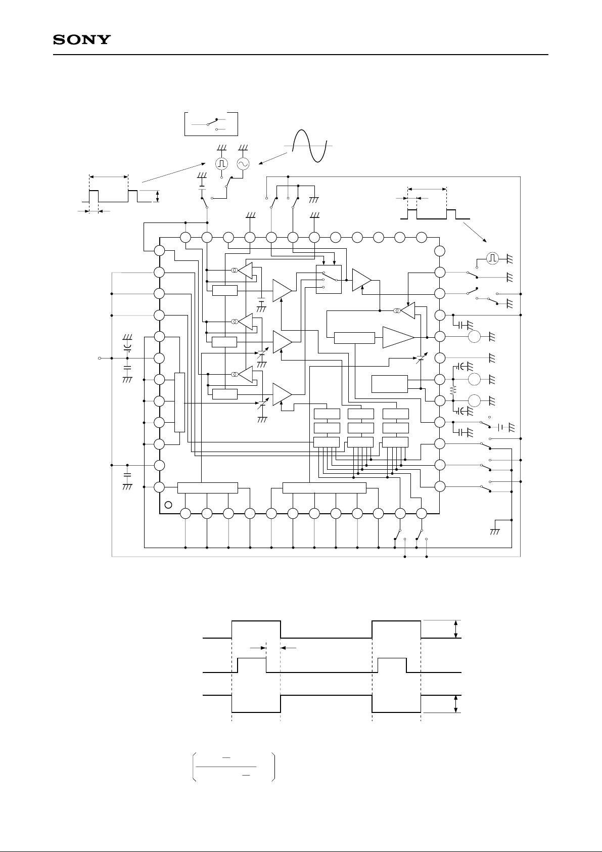
Electrical Characteristics Measurement Circuit
CXA2027Q
11.5µs
5V
63.6µs
3.32V
47µ
0.01µ
0.01µ
SW polarity
Vx
37
38
39
40
41
42
43
44
45
46
47
48
3.32V
36
D/A
35
D/A
SG35-2
SW35-1
34
S/H
S/H
S/H
a
b
SW35-2
33
SG35-1
32
GCA
GCA
GCA
SW32
SW31
31
30
f = 1MHz
3.12V
DC + 0.4Vp-p
29
GCA
DC shift
LOG
D/A
LATCH LATCH
D/A
LOG
D/A D/A
2728
7µs
Driver
REF
V
LOG
LATCH
63.6µs
5V
0V
26
25
24
23
22
SW22-1
21
0.01µ
20
19
18
17
1µ
16
0.47µ
15
14
13
SW23
1µ
300
SG23
SW22-2
V20
V18
V17
3.1V
SW16
SW15
SW14
SW13
Note 2: No. 12, 13
Line clamp pulse SG23
Input SG35-2
Output V20
Defined as:
2
3
1
V20 ( Vx)
2
V20 (Vx) ×
5
4
–1 × 100 [%].
1
2
6
4µs
9
8
7
10
11
SW11
121
SW12
Vx
V20 (Vx)
No. 12 Vx = 1.5V
No. 13 Vx = 0.3V
– 10 –
Page 11

CXA2027Q
Pulse Timing
[Pulse Timing 1 (pixel units)]
CLP pulse and SH pulse
Input the SH pulse at the end of the effective signal so as not to be affected by signal fluctuation caused by
the clamp.
SH pulse and MPX pulse (MPX1, MPX2)
Input the SH pulse in sync with the reference channel.
MPX1 pulse and MPX2 pulse
Delay the timing of MPX2 when G changes to B. (Table 1, t3)
CCD signal
(R-IN/
G-IN/
B-IN)
CLP
SH
MPX1
MPX2
SIGOUT
Reset level
Precharge level
t2
t4
Effective signal level
t1
50%
50%
tr = tf = 5ns
50%
t3
50%
t5
Data taken in at
AD converter
Output channel
BRGBR
Min. Typ. Max.
t1
t2
t3
t4
t5
100ns
40ns
5ns
5ns
50ns
20ns
60ns
Table 1
– 11 –
Page 12
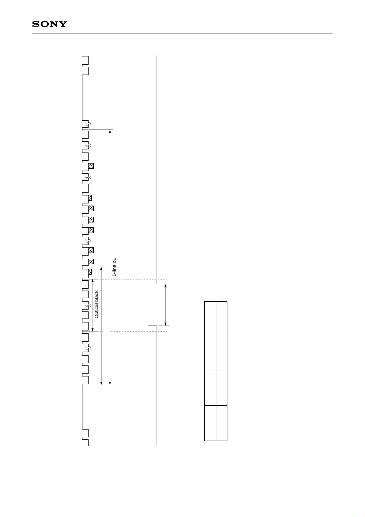
CXA2027Q
1-line output period
Optical black
Dummy signal
The LCLP pulse is recommended to be applied during the optical black period.
t6
Max.
Table 2
Min. Typ.
t6 10µs
B-IN)
G-IN/
(R-IN/
[Pulse Timing 2 (line units)]
CCD signal
LCLP
– 12 –
Page 13
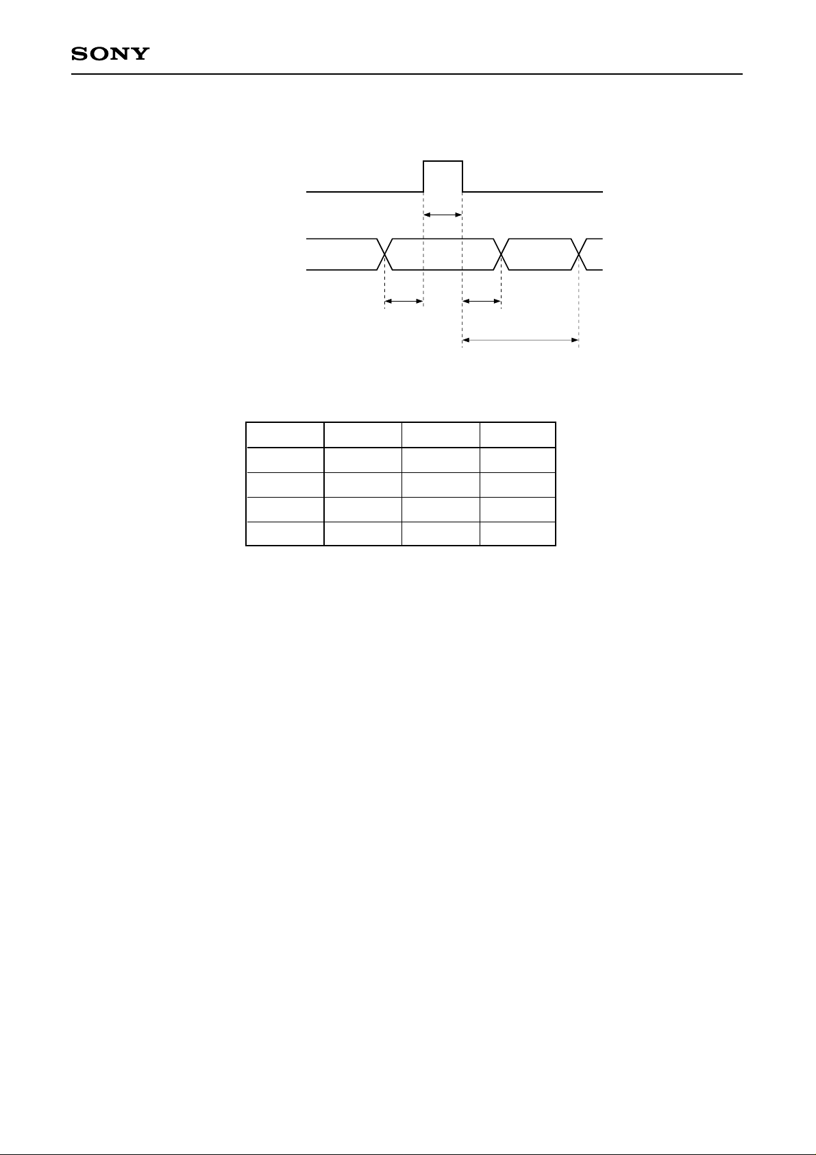
[Pulse Timing 3 (latch data input)]
Latch gate
(LPR/LPG/LPB)
Input data
(LD0 to LD4)
CXA2027Q
t8
t7 t9
t7
t8
t9
t10
(input data decision time)
t10
Min. Typ. Max.
50ns
50ns
50ns
800ns
Table 3
– 13 –
Page 14

Notes on Operation
1. Pre-stage GCA
The gain characteristics is as given in page 16. As a guideline, the calculation formula is 0.5 × 1.05n[times]
(n = 0 to 31: n is D/A converter input in decimal).
2. Post-stage GCA
The gain characteristics is as given in page 16. When the GC pin is open, gain becomes approximately
double.
3. Line clamp
When the LCLP pulse (line clamp pulse) is made high during the optical black period of CCD output, output
(Pin 20) is clamped approximately to VRB (= 2.0V) voltage.
4. Pixel clamp
The pixel clamp function (at Pins 35, 36 and 37) requires large charging and discharging current through
the capacitor, therefore, keep the ground area below the emitter follower as wide as possible. The distance
between the input capacitor and input pin should also be as short as possible.
CXA2027Q
5. DC offset adjustment between channels
There is a slight difference between clamp voltages (black level voltage) of different channels due to
component scatterings within the IC. Correct the B and G channel DC levels relative to R channel using
D4-0 to D4-4 and D5-0 to D5-4. The adjustment step for the input pins (Pins 36 and 37) is approximately
5mV/LSB. The standard settings are D4-0 to D4-3 = “L”, D4-4 = “H”, and D5-0 to D5-3 = “L”, D5-4 = “H”.
6. Output DC voltage adjustment
Output (Pin 20) clamp voltage varies slightly due to variations within the IC. Adjust output clamp voltage
using D6-0 to D6-5. The adjustment step is approximately 1mV/LSB. The standard settings are D6-0, D6-1
= “H”, D6-2 to D6-5 = “L”.
7. Pulse input signals
Sharp edges at input pulse signals may affect output. If there is a problem, insert a damping resistor
(around 100 to 200Ω) to smooth the pulse’s edges.
– 14 –
Page 15

A/D Converter
CXA2027Q
5V
Pulse input
Digital data input
Pulse input
47µF
LCLP
GC
MPX2
MPX1
D4-4
D4-3
D4-2
D4-1
D4-0
D5-4
D5-3
D5-2
D5-1
D5-0
(N.C.)
(N.C.)
SH
CLP
23
22
32
31
46
45
44
43
41
4
3
2
1
48
26
24
33
30
0.1µF
47
42
VCCD
VCCA
DA5 (5bit) DA4 (5bit)
TD5
TD4
21
19
GND
VCCP
SW (cont)
× 0.5 to 2.27
GCA1
SH1
VIN
SIGOUT
20
Driver
DC shift
GCA
× 1 to 3
GCA2
× 0.5 to 2.27
SH2
CLPC
16
0.47µF
GCA3
× 0.5 to 2.27
SH3
VRT
LOG
LOG
VRT
18
REF
VOLTAGE
LOG
VRB
1µF
VRB
1µF
17
DA2 (5bit) DA3 (5bit)
DA1 (5bit)
TD6
DA6 (6bit)
BUF
TD3
TD2
TD1
LATCH3
LATCH2
LATCH1
25
10
9
8
7
6
5
34
29
28
27
40
15
14
13
12
11
39
38
(N.C.)
D6-5
D6-4
D6-3
D6-2
D6-1
D6-0
(N.C.)
(N.C.)
(N.C.)
(N.C.)
LPB
LD4
LD3
LD2
LD1
LD0
LPG
LPR
Application circuits shown are typical examples illustrating the operation of the devices. Sony cannot assume responsibility for
any problems arising out of the use of these circuits or for any infringement of third party patent and other right due to same.
Digital data pulse input Digital data input
Application Circuit
12V
R-IN
100Ω
VOUT-R
35
1000pF
2.2kΩ
12V
G-IN
100Ω
VOUT-G
36
2.2kΩ
– 15 –
1000pF
37
B-IN
12V
100Ω
1000pF
2.2kΩ
VOUT-B
CCD Linear Image Sensor
Page 16
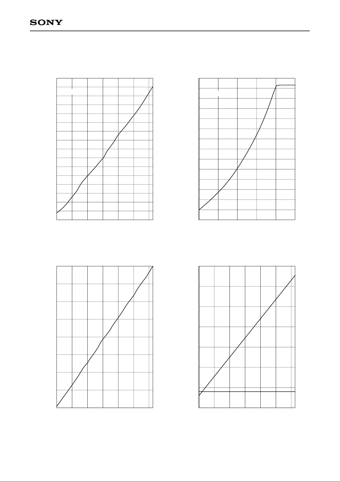
Example of Representative Characteristics (VCC = 5V, Ta = 25°C)
CXA2027Q
Pre-stage GCA gain characteristics data (unit)
9
8
f = 1MHz
7
6
5
4
3
2
1
Gain [dB]
0
–1
–2
–3
–4
–5
–6
–7
0 5 10 15 20 25 30
LD0 to LD4 input data (expressed as decimal system)
Post-stage GCA gain characteristics data (unit)
12
11
10
Gain [dB]
–1
–2
f = 1MHz
9
8
7
6
5
4
3
2
1
0
012345
GC pin input voltage [V]
G, B channels clamp voltage adjustment range
80
60
40
20
0
–20
–40
Difference from R channel clamp voltage [mV]
–60
–80
0 5 10 15 20 25 30
D4-0 to D4-4 or D5-0 to D5-4 input data (expressed as decimal system)
SIGOUT clamp voltage adjustment range
2060
2050
2040
2030
2020
SIGOUT voltage [mV]
2010
2000
1990
0 102030405060
D6-0 to D6-5 input data (expressed as decimal system)
VRB
– 16 –
Page 17
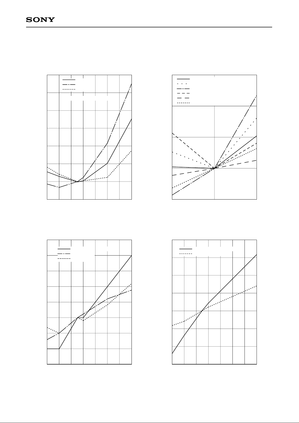
Example of Temperature and Supply Voltage Fluctuation Characteristics
CXA2027Q
Total gain temperature characteristics fluctuation
0.3
5V
5.25V
0.25
0.2
0.15
0.1
Gain fluctuation [dB]
0.05
0
–0.05
01020406070
4.75V
LD0 to LD4 = 0, GC = open
30 50
Temperature [°C]
Total gain supply voltage fluctuation
0.15
DA1, 2, 3 = all 0/GC = VCC
DA1, 2, 3 = all 0/GC = open
DA1, 2, 3 = all 0/GC = GND
DA1, 2, 3 = all 1/GC = VCC
DA1, 2, 3 = all 1/GC = open
DA1, 2, 3 = all 1/GC = GND
0.1
0.05
Gain fluctuation [dB]
0
–0.05
4.75 5.25
Ta = 25°C
f = 1MHz
5
Vcc [V]
VRT, VRB temperature characteristics voltage fluctuation
2.5
VRT
2
1.5
1
0.5
0
Fluctuation voltage [mV]
–0.5
–1
–1.5
VRB
VRT – VRB
01020406070
30 50
Temperature [°C]
VCC = 5V
Clamp voltage temperature characteristics fluctuation
2
SIGOUT
SIGOUT – VRB
1.5
1
0.5
0
SIGOUT fluctuation voltage [mV]
–0.5
–1
–1.5
01020 40 6070
30 50
Temperature [°C]
VCC = 5V
– 17 –
Page 18

Package Outline Unit: mm
15.3 ± 0.4
CXA2027Q
48PIN QFP (PLASTIC)
+ 0.4
12.0 – 0.1
2536
37
48
112
0.8 0.3 – 0.1
+ 0.15
24
13
± 0.12
M
+ 0.35
2.2 – 0.15
+ 0.1
0.15 – 0.05
0.15
+ 0.2
0.1 – 0.1
13.5
0.9 ± 0.2
PACKAGE STRUCTURE
EPOXY RESIN
SOLDER / PALLADIUM
PLATING
COPPER / 42 ALLOY
0.7g
SONY CODE
EIAJ CODE
JEDEC CODE
QFP-48P-L04
∗QFP048-P-1212-B
PACKAGE MATERIAL
LEAD TREATMENT
LEAD MATERIAL
PACKAGE WEIGHT
NOTE : PALLADIUM PLATING
This product uses S-PdPPF (Sony Spec.-Palladium Pre-Plated Lead Frame).
– 18 –
 Loading...