

Page 1
Dual REC/PB Preamplifier
Description
The CXA2500M/N is a dual recording/playback preamplifier system bipolar IC which has been developed
for the low voltage operating cassette tape recorder.
Features
• Low quiescent current (VCC = 2V)
PB: ICC = 3.2mA (typ.)
REC: ICC = 5.2mA (typ.)
• Very few external parts
• Built-in Metal/Normal selection switch
• Small switching noise due to internal transient
muting
Applications
3V headphone radio cassette recorders
Structure
Bipolar silicon monolithic IC
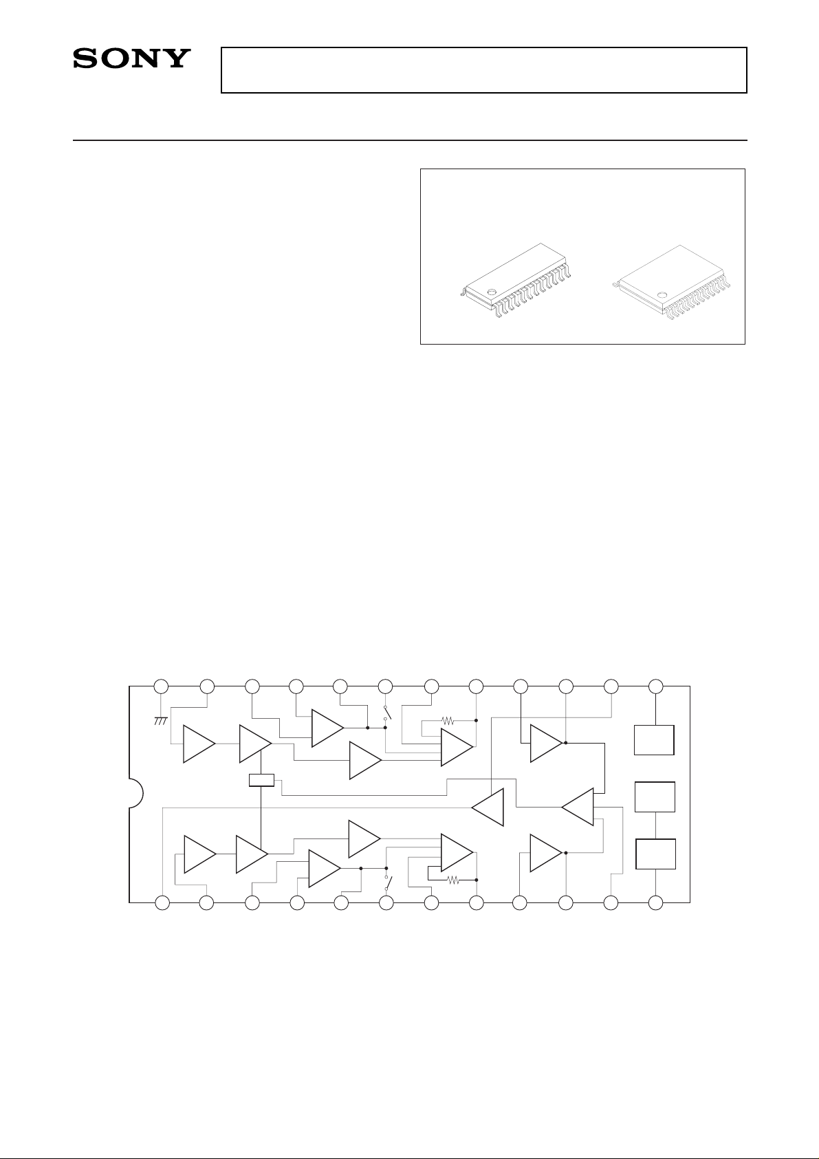
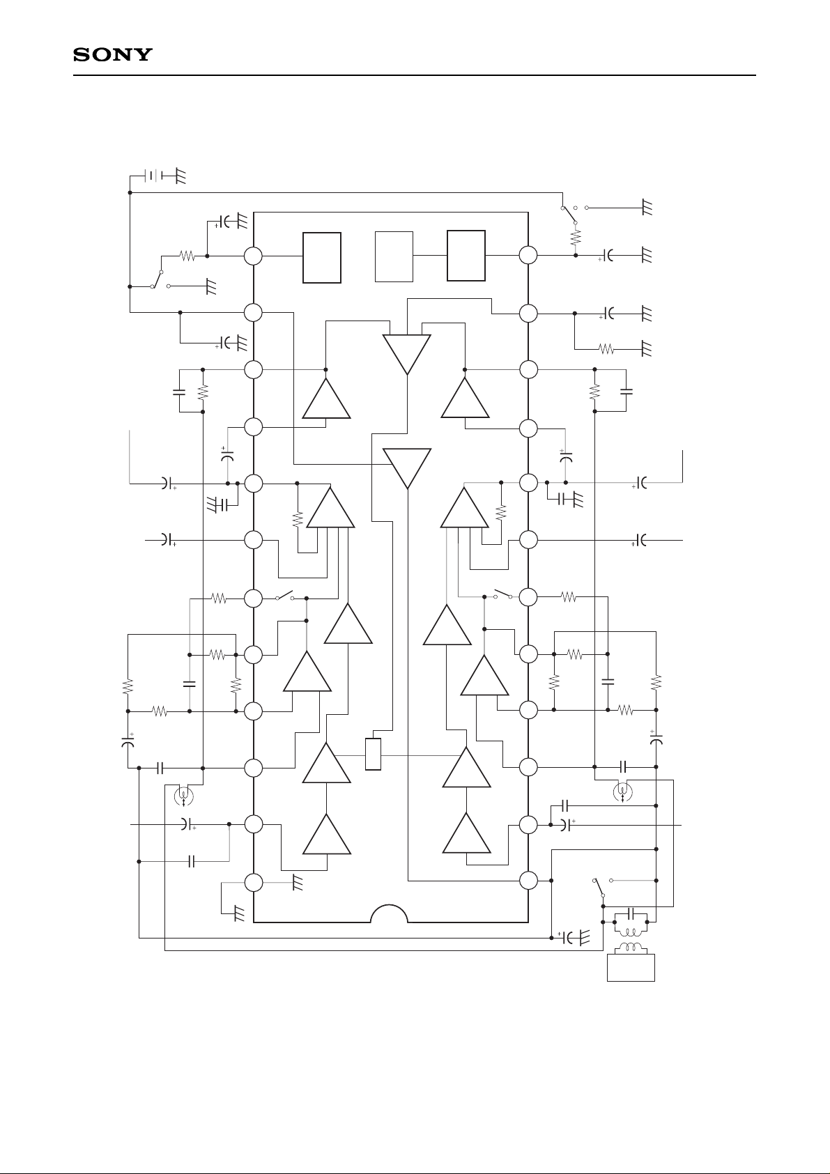
Bock Diagram
Absolute Maximum Ratings (Ta = 25°C)
• Supply voltage VCC 7V
•Operating temperature Topr –20 to +75 °C
• Storage temperature Tstg –65 to +150 °C
• Allowable power dissipation PD
CXA2500M 600 mW
CXA2500N 470 mW
Operating Conditions
Supply voltage PB VCC 1.2 to 3.5 V
REC VCC 1.6 to 3.5 V
– 1 –
E94806B8Y
Sony reserves the right to change products and specifications without prior notice. This information does not convey any license by
any implication or otherwise under any patents or other right. Application circuits shown, if any, are typical examples illustrating the
operation of the devices. Sony cannot assume responsibility for any problems arising out of the use of these circuits.
CXA2500M/N
REFERENCE
MIC INPUT (A)
PB PRE
INPUT (A)
PB NF (A)
PB OUTPUT (A)
PB EQ
SWITCH (A)
TUNER
INPUT (A)
LINE
OUTPUT (A)
REC DRIVE
INPUT (A)
REC DRIVE
OUTPUT (A)
AGC TIME
CONSTANT
TAPE/TUNER
SELECTOR
GROUND
MIC INPUT (B)
PB PRE
INPUT (B)
PB NF (B)
PB OUTPUT (A)
PB EQ
SWITCH (B)
TUNER
INPUT (B)
LINE
OUTPUT (B)
REC DRIVE
INPUT (B)
REC DRIVE
OUTPUT (B)
V
CC
PB/REC
SELECTOR
6dB
22dB
12dB
–0.3dB
20.5dB
MIC
GCA
PB
LINE
REC
AMP
REF
PB/
REC
NORM/
METAL
TAPE/
TUNER
AGC
LINE
AMP
PB
GCA
MIC
REC
AGC
DET
2
3
4
5
6
7
8
9
10
11
12
13
1415
16
17
18
19
20
21
22
23
24
1
CXA2500M
24 pin SOP (Plastic)
CXA2500N
24 pin SSOP (Plastic)
Page 2
– 2 –
CXA2500M/N
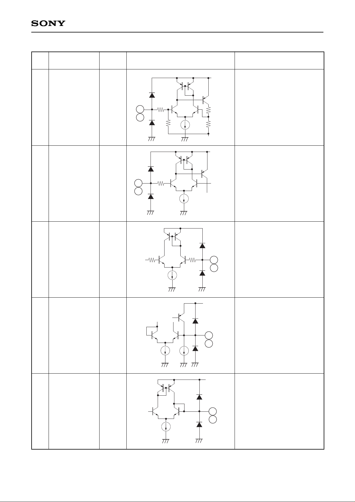
Pin Description Pin voltage is during VCC = 2V
No.
223MIC IN (A)
MIC IN (B)
0.93V MIC preamplifier input
PB preamplifier input
PB equalizer circuit negative
feedback
PB preamplifier output
PB equalizer switch
0.93V
0.93V
0.93V
0.93V
PB PRE IN (A)
PB PRE IN (B)
PB-NF (A)
PB-NF (B)
PB OUT (A)
PB OUT (B)
PB EQ SW (A)
PB EQ SW (B)
3
22
4
21
5
20
6
19
Symbol
Voltage
(Typ.)
Equivalent circuit Description
510
10k
20k
20k
VCC
Vref
2
23
510
VCC
Vref
22
3
510
VCC
Vref
510
4
21
VCC
20
5
VCC
6
19
Page 3
– 3 –
CXA2500M/N
No.
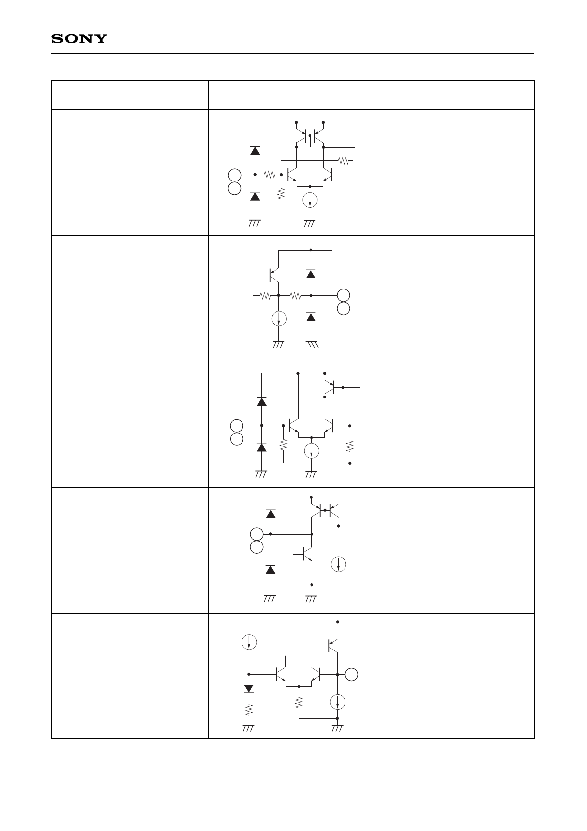
718TUNER IN (A)
TUNER IN (B)
0.93V Tuner input
Line amplifier output
REC drive input
REC drive output
Reference voltage output
0.58V
0.93V
1.0V
0.93V
LINE OUT (A)
LINE OUT (B)
REC AMP IN (A)
REC AMP IN (B)
REC AMP OUT
(A)
REC AMP OUT
(B)
REF
8
17
9
16
10
15
1
Symbol
Voltage
(Typ.)
Equivalent circuit Description
40k
4k
VCC
Vref
40k
18
7
142
40k
VCC
8
17
10k
4k
VCC
Vref
16
9
VCC
10
15
VCC
1
Page 4
– 4 –
CXA2500M/N
No.
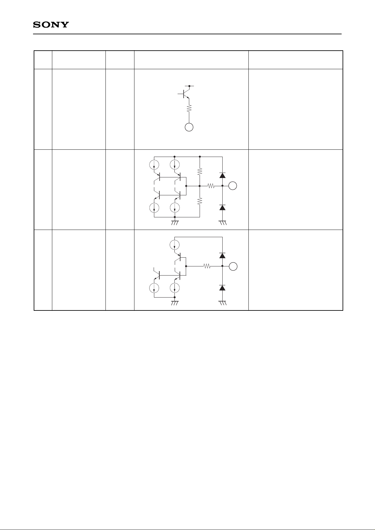
11 AGC TC 0.37V AGC time constant
Tape/tuner selection
During Tape/Normal: 0V
During Tape/Metal: 0.5V
During Tuner Mode: 2.0V
PB/REC selection
During PB = 0V
During REC = 2.0V
0.5V
(Open)
0V
(2.0V)
TAPE/TUNER
PB/REC
12
13
Symbol
Voltage
(Typ.)
Equivalent circuit Description
1k
VCC
11
150k
VCC
142
50k
12
VCC
142
13
Page 5
– 5 –
CXA2500M/N
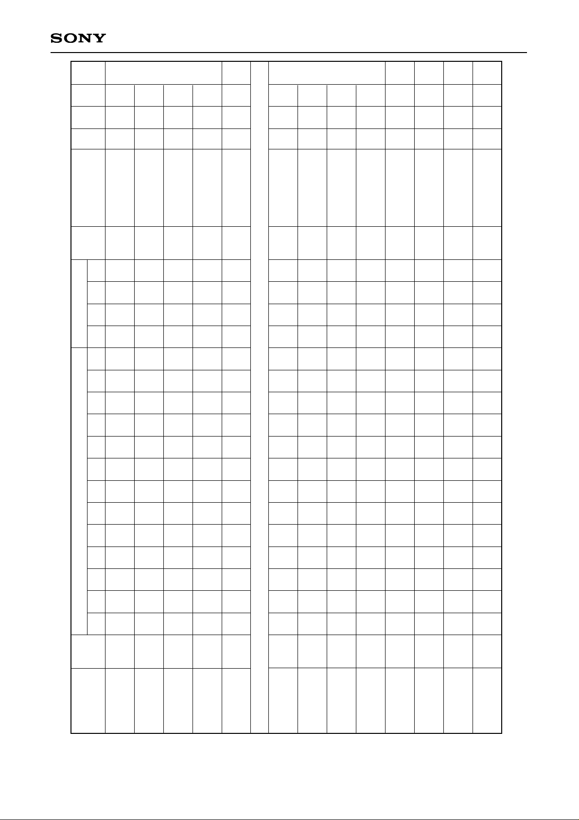
Electrical Characteristics VCC = 2.0V, f = 1kHz, Ta = 25°C, unless otherwise specified.
Item
Icq1
Icq2
Icq3
Icq4
Vref
Gvo
Gvc1
Gvc2
CB
THD
Vom
Vno
RR
A
A
A
A
A
A
A
A
A
A
A
A
B
OFF
OFF
OFF
OFF
ON
ON
ON
ON
ON
ON
ON
ON
ON
PB
REC
PB
REC
PB
PB
PB
PB
PB
PB
PB
PB
PB
C
C
A
A
C
C
C
B
C
C
C
C
C
OFF
OFF
OFF
OFF
OFF
OFF
OFF
OFF
OFF
OFF
OFF
OFF
OFF
A
A
A
A
A
A
A
A
A
A
A
A
A
OFF
OFF
OFF
OFF
OFF
ON
ON
ON
ON
ON
ON
OFF
OFF
OFF
OFF
OFF
OFF
OFF
ON
ON
ON
ON
ON
ON
OFF
OFF
B
B
B
B
B
A
B
B
B
B
B
B
B
B
B
B
B
B
A
B
B
B
B
B
B
B
B
B
B
B
B
B
B
B
B
B
B
B
B
B
B
B
B
B
B
B
B
B
B
B
B
B
A
A
A
A
A
A
A
A
A
A
A
A
A
dBm
dBm
dBm
dBm
dBm
Io
Io
Io
Io
V1
e8, e17
e8, e17
e8, e17
e8, e17
e8, e17
e8, e17
e8, e17
e8, e17
Vcc = 2.0V
No signal, Tape
Vcc = 2.0V
No signal, Mic Rec
Vcc = 2.0V
No signal, Tuner
Vcc = 2.0V
No signal, Tuner Rec
Vcc = 2.0V
No signal, Tape
Vo = –15dBm
Vo = –15dBm
Vo = –15dBm
Vo = –15dBm
Vo = –15dBm
THD = 1%
Rg = 2.2kΩ
fr = 100Hz
Vr = –30dBm
1.8
3.8
1.3
2.8
0.78
54
28.5
25.5
–2.0
—
190
—
27.5
3.2
5.2
2.8
4.2
0.93
65
30.8
27.2
0
0.3
300
72
35
5.5
7.2
4.7
6.2
1.05
—
33.0
29.0
+2.0
1.05
—
125
—
mA
V
dB
%
mV
µV
dB
Symbol
SW condition Input condition
Measure
-ment
point
Measurement
conditions
Min. Typ. Max. Unit
S1 S2 S3 S4 S5 S6 S7 S8 S9 S10 S11 S12 S13 Vin1 Vin2 Vin3 Unit
Tape playback
quiescent current
MIC recording
quiescent current
Radio playback
quiescent current
Radio pecording
quiescent current
Reference
voltage
(1) PLAYBACK MODE
Open loop
voltage gain
Close loop
voltage gain 1
Close loop
voltage gain 2
Channel
balance
Total harmonic
distortion
Maximum output
voltage
Output noise
voltage
Ripple rejection
Page 6

– 6 –
CXA2500M/N
Gvc
CB
THD
Vom
Vno
RR
Gvc
CB
THD
Vno
W ALC
Vo ALC
CB ALC
RR
A
A
A
A
A
B
A
A
A
A
A
A
A
B
ON
ON
ON
ON
ON
ON
ON
ON
ON
ON
ON
ON
ON
ON
REC
REC
REC
REC
REC
REC
REC
REC
REC
REC
REC
REC
REC
REC
A
A
A
A
A
A
C
C
C
C
C
C
C
C
OFF
OFF
OFF
OFF
OFF
OFF
ON
ON
ON
OFF
ON
ON
ON
OFF
A
A
A
A
A
A
B
B
B
A
B
B
B
A
OFF
OFF
OFF
OFF
OFF
OFF
OFF
OFF
OFF
OFF
OFF
OFF
OFF
OFF
OFF
OFF
OFF
OFF
OFF
OFF
OFF
OFF
OFF
OFF
OFF
OFF
OFF
OFF
B
B
B
B
B
B
B
B
B
B
B
B
B
B
B
B
B
B
B
B
B
B
B
B
B
B
B
B
A
A
A
A
B
B
B
B
B
B
B
B
B
B
A
A
A
A
B
B
B
B
B
B
B
B
B
B
A
A
A
A
A
A
C
C
A
A
A
A
A
A
–50
–60
–60
–30
–30
–30
dBm
dBm
dBm
dBm
dBm
dBm
dBm
dBm
e10, e15
e10, e15
e10, e15
e10, e15
e10, e15
e10, e15
e10, e15
e10, e15
e10, e15
e10, e15
e10, e15
e10, e15
e10, e15
e10, e15
Vin = –30dBm
Vin = –30dBm
Vin = –30dBm
THD = 1%
Rg = 10kΩ
fr = 100Hz
Vr = –30dBm
Vo = –15dBm
Vo = –15dBm
Vin = –50dBm
BW = 30 to 20kHz
The input range
when the output
level varies ±3dB
from the standard
input level
(Vin = –60dBm)
Vin = –60dBm
Vin = –60dBm
fr = 100Hz
Vr = –30dBm
17.8
–1.5
—
380
—
24
58.5
–1.5
—
—
—
230
–2
–5
19.5
0
0.1
600
280
33
61.8
0
1.5
3
39
340
0
3
21.2
1.5
0.5
—
360
—
65.0
1.5
4.5
4.7
—
470
+2
—
dB
%
mV
µV
dB
dB
%
mV
dB
mV
dB
S1 S2 S3 S4 S5 S6 S7 S8 S9 S10 S11 S12 S13 Vin1 Vin2 Vin3 Unit
Item Symbol
SW condition Input condition
Measure
-ment
point
Measurement
conditions
Min. Typ. Max. Unit
(2) RADIO RECORDING: -
Voltage gain
Channel balance
Total harmonic
distortion
Maximum output
voltage
Output noise
voltage
Ripple rejection
(3) MIC RECORDING: -
Voltage gain
Channel
balance
Total harmonic
distortion
Output noise
voltage
ALC width
ALC voltage
ALC balance
Ripple rejection
Page 7

– 7 –
CXA2500M/N
Measurement Circuit
REF
MIC
IN (A)
PB PRE
IN (A)
PB/MIC
NF (A)
PB
OUT (A)
METAL
SW (A)
TUNER
IN (A)
LINE
OUT (A)
REC
IN (A)
REC
OUT (A)
AGC TC
TAPE/
RADIO SW
GND
MIC
IN (B)
PB PRE
IN (B)
PB/MIC
NF (B)
PB
OUT (B)
METAL
SW (B)
TUNER
IN (B)
LINE
OUT (B)
REC
IN (B)
REC
OUT (B)
V
CC
REC/PB
SW
Vin1
1kHz
S5
S7
1µ
Vin2
1kHz
1µ
2.2k
330
33µ
S9
A
B
100k
15k
22k
1µ
Vin3
1kHz
A
B
10k
1µ
10k
1µ
e8
10k
0.0047µ
e10
4.7µ
S13
A
B
ABC
S4
TUNER
METAL PB
NORMAL PB
10k
S3
PB
S2
I
0
47µ
A
B
Vr
2V
10k
0.0047µ
e15
400 to 30kHz
BPF
e17
1µ
1µ
1kHz
Vin3
10k
10k
1µ
15k
100k
330
A
B
S12
22k
33µ
2.2k
1µ
1kHz
Vin2
1µ
1kHz
Vin1
S6
100µ
V1
S11
A
B
S10
S8
2V
S1
VCC
VCC
2.2k
I
11
2
3
4
5
6
7
8
9
10
11
12
13
1415
16
17
18
19
20
21
22
23
24
1
0.01µ
0.01µ
C
REC
400 to 30kHz
BPF
400 to 30kHz
BPF
400 to 30kHz
BPF
Page 8
– 8 –
CXA2500M/N
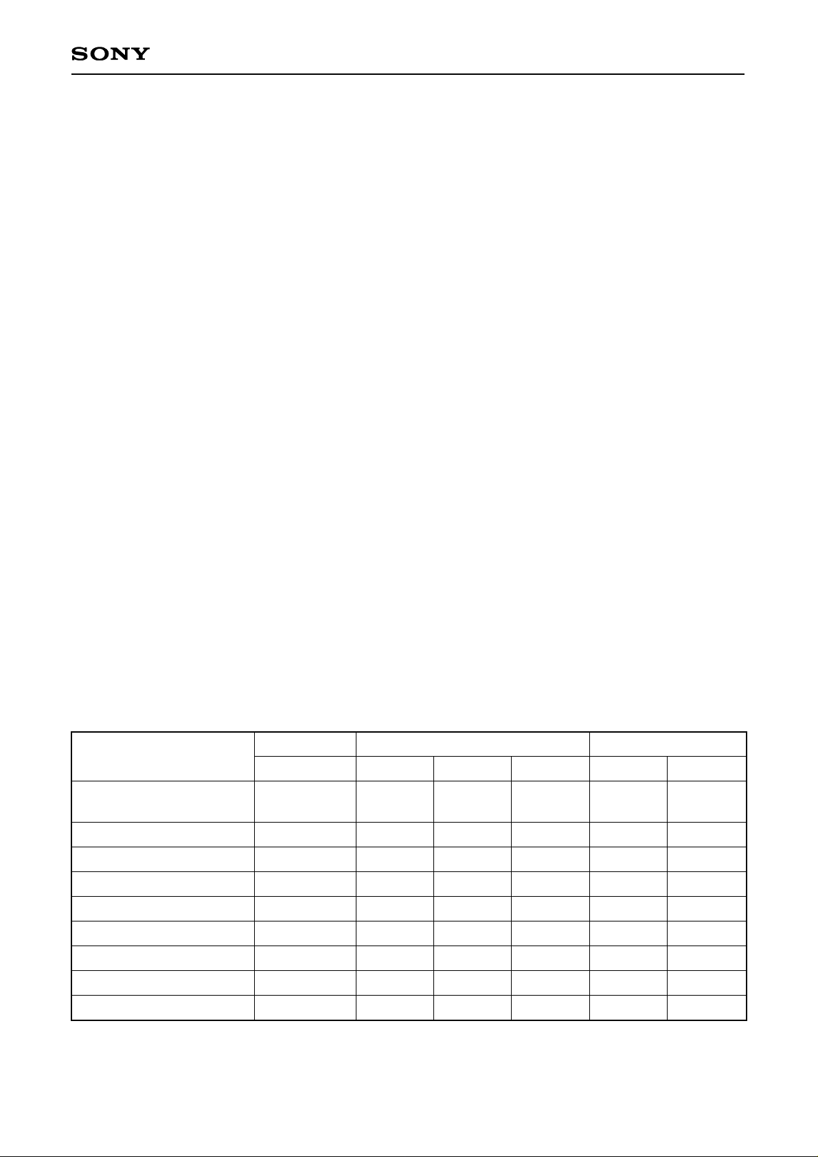
Application Circuit
6dB 22dB
12dB
–0.3dB
20.5dB
MIC
GCA
PB
LINE
REC
AMP
REF
PB/
REC
NORM/
METAL
TAPE/
RADIO
AGC
LINE
AMP
PB
GCA
MIC
REC
AGC
DET
1µ
A CH
1000p
MIC IN (A)
330
33µ
15k
330k
39k
0.01µ
22k
RADIO IN (A)
1µ
TO POWER AMP (A)
1µ
10k
0.0047µ
3.3M
47µ
22µ
2.2k
RADIO
TAPE/METAL
TAPE/NORM
10k
22µ
PB
47µ
10k
0.0047µ
1µ
1µ
TO POWER AMP (B)
1µ
RADIO IN (B)
22k
15k
330k
0.01µ
39k
330
1000p
MIC IN (B)
1µ
BIAS
100µ
REC
PB
1µ
VCC
33µ
0.01µ
0.01µ
2
3
4
5
6
7
8
9
10
11
12
13
14
15
16
17
18
19
20
21
22
23
24
1
0.01µ
0.01µ
REC
Application circuits shown are typical examples illustrating the operation of the devices. Sony cannot assume responsibility for
any problems arising out of the use of these circuits or for any infringement of third party patent and other right due to same.
Page 9
– 9 –
CXA2500M/N
Description of Operation
REF Pin (Pin 1)
A low impedance pin for outputting the internal reference voltage, which is fixed at 0.93V regardless of
supply voltage variation.
LINE OUT Pin (Pin 8)
This output pin outputs signal from any selected source (MIC, Tape or Tuner) to the subsequent stages
such as Dolby NR or power amplifier for further signal processing. It is internally biased at 0.58V so as to
achieve maximum dynamic swing at minimum supply voltage of 1.2V. The change of DC potential at this
pin that may result from any changeover of PB/REC or Tape/Tuner switch was set to be minimum, thus
reducing any potential occurence of switching noise.
REC Out Pin (Pin 10)
This recording driver output pin is internally biased at 1.0V to achieve maximum signal swing at minimum
supply voltage of 1.6V during the recording mode. The REC OUT will be momentally muted during the
changeover of PB/REC or Tape/Tuner modes, so as to prevent mis-recording of any undesired switching
noise. The muting period is determined by the values of R and C at Pins 12 or 13.
AGC TC Pin (Pin 11)
This is the external pin for AGC filter during the MIC Recording mode. The attack time is determined by the
1kΩ resistor inside the IC and the external electrolytic capacitor. The recovery time is determined by both
external resistor and electrolytic capacitor at Pin 11.
Notes on Operation
1. The following table shows the potential at Pins 12 and 13 and the associated operating states of the
amplifier. Each of the pins, when at the same potential as Pin 14, has H level, and when at the same
potential as Pin 24, has L level.
System Control Operation Table
Control pins
Amplifier operating state
MIC AMP
AGC DET
GCA
AMP
PB AMP
EQ SWITCH
LINE AMP
REC AMP
OFF
OFF
OFF
OFF
ON
OFF
ON
OFF
OFF
OFF
OFF
OFF
ON
ON
ON
OFF
OFF
OFF
OFF
OFF
OFF
OFF
ON
OFF
ON
ON
ON
ON
OFF
OFF
ON
ON
OFF
OFF
OFF
OFF
OFF
OFF
ON
ON
Operating
mode
Playback
(Normal)
Playback
(Metal)
Tuner
Mode
MIC
Recording
Tuner
Recording
Pin 13 L H
Pin 12 L FLOAT H L, FLOAT H
Page 10
– 10 –
CXA2500M/N
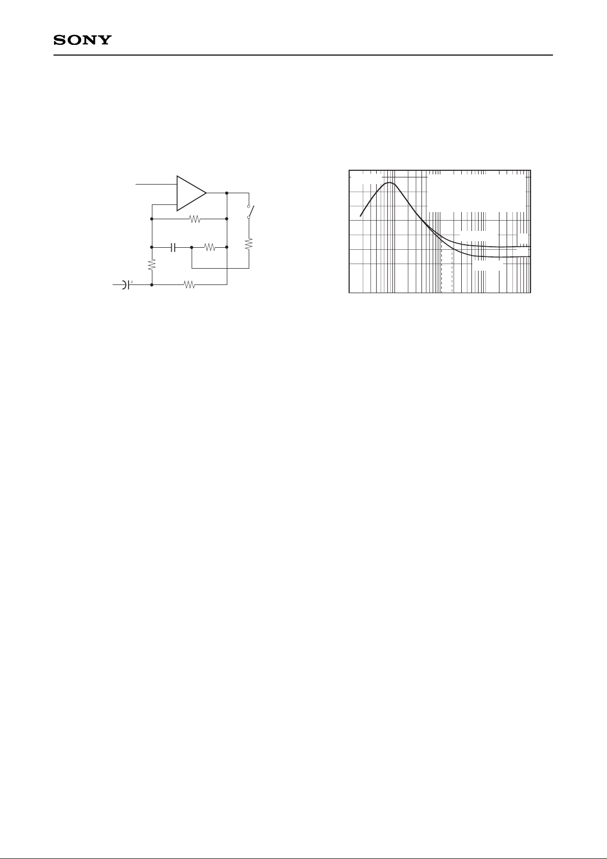
2. PB Mode:
To reduce the PB amplifier DC output offset, it is recommended that 39kΩ resistor be connected as shown
in the Application Circuit. However, too low this resistor value may affect the low frequency portion of the
PB frequency response. The inter-relationship of the RC values in the playback equalization network is as
shown below:
During Normal PB mode,
Gain G1 = 20 log (R2 + R5)/R5
3dB cut-off frequency, f1 = 1/(2 × 3.1416 × C1 × R2)
During Metal PB mode,
Gain G2 = 20 log (R2//R3 + R5)/R5
3dB cut-off frequency, f2 = 1/(2 × 3.1416 × C1 × R2//R3)
3. Use of RC at Tape/Tuner and PB/REC pins:
The purpose of the external RC components at the switch inputs is to create an internal mute pulse so as to
mute the REC OUT momentally during the switching operation. By doing so, the switching click noise that
may appear at REC OUT can be reduced. The selection of the RC values affects the duration of the mute
pulse. It is recommended to use resistor of 2.2kΩ and below at Tape/Tuner pin, i.e Pin 12. These RC
components may be removed if such internal pop noise countermeasure is not required.
R1
330k
C1
0.01µ
IN
R2
15k
R3
22k
R5
330
REF
R4
39k
C2
33µ
PB
+
–
55
50
40
30
Voltage [dB]
CXA2500
TAPE PB: GV, THD vs f
VO = –15dBm
VCC = 2V
45
35
25
10 100 1k 10k 100k
f
1 f2
f [Hz]
NORMAL
METAL
G1
G2
GV (dB)
Page 11
– 11 –
CXA2500M/N
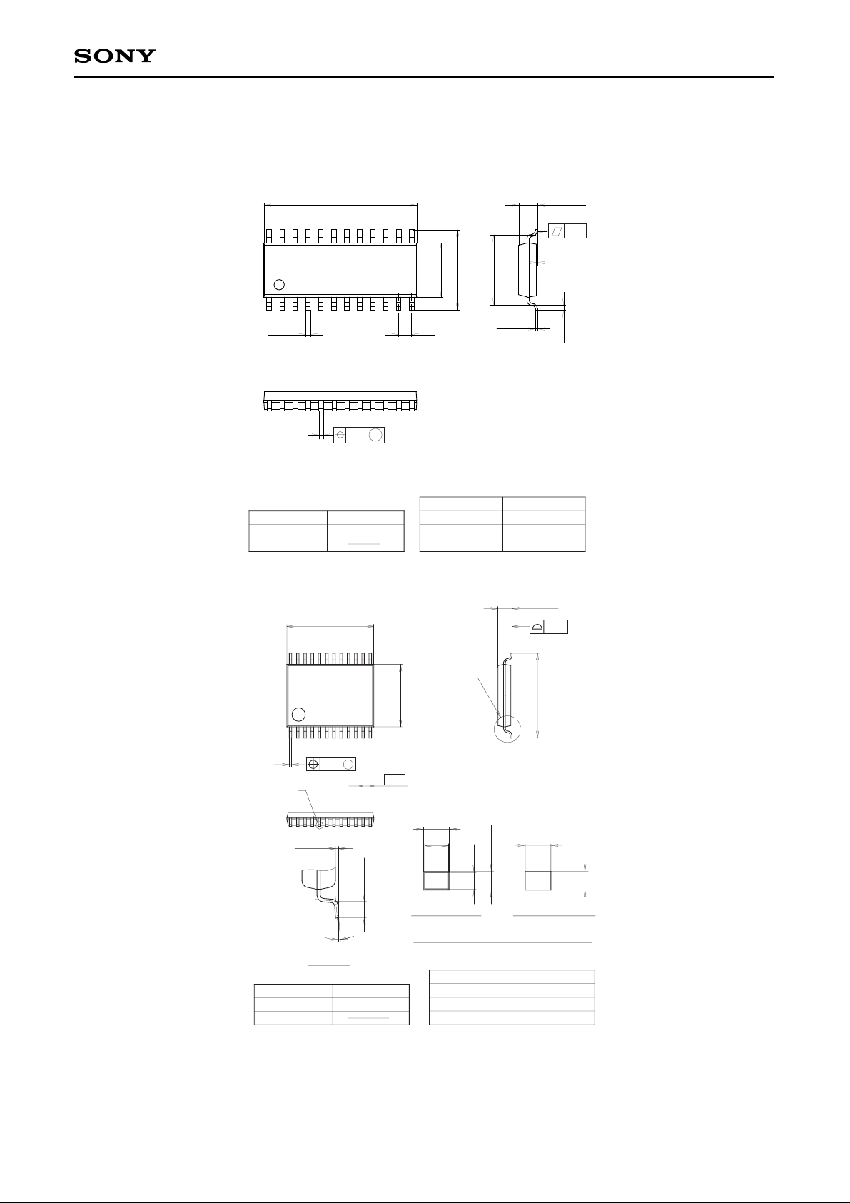
Package Outline Unit: mm
CXA2500M
CXA2500N
SONY CODE
EIAJ CODE
JEDEC CODE
M
PACKAGE STRUCTURE
MOLDING COMPOUND
LEAD TREATMENT
LEAD MATERIAL
PACKAGE WEIGHT
EPOXY/PHENOL RESIN
SOLDER PLATING
COPPER ALLOY / 42ALLOY
24PIN SOP (PLASTIC)
15.0 – 0.1
+ 0.4
1 12
1324
1.270.45 ± 0.1
5.3 – 0.1
+ 0.3
7.9 ± 0.4
0.2 – 0.05
+ 0.1
0.5 ± 0.2
0.1 – 0.05
+ 0.2
0.15
1.85 – 0.15
+ 0.4
6.9
± 0.12
SOP-24P-L01
∗SOP024-P-0300-A
0.3g
SONY CODE
EIAJ CODE
JEDEC CODE
SSOP-24P-L01
SSOP024-P-0056
PACKAGE MATERIAL
LEAD TREATMENT
LEAD MATERIAL
PACKAGE MASS
EPOXY RESIN
SOLDER/PALLADIUM
42/COPPER ALLOY
PACKAGE STRUCTURE
PLATING
0.1g
24PIN SSOP(PLASTIC)
0.1 ± 0.1
0° to 10°
0.5 ± 0.2
DETAIL
A
∗5.6 ± 0.1
24
∗7.8 ± 0.1
13
0.65
12
1
7.6 ± 0.2
0.1
1.25 – 0.1
+ 0.2
A
0.13
M
NOTE: Dimension “∗” does not include mold protrusion.
b=0.22 – 0.05
+ 0.1
0.15 – 0.02
+ 0.05
(0.22)
(0.15)
0.15 – 0.01
DETAIL B : SOLDER DETAIL B : PALLADIUM
+ 0.03
b=0.22 ± 0.03
B
b
NOTE : PALLADIUM PLATING
This product uses S-PdPPF (Sony Spec.-Palladium Pre-Plated Lead Frame).
 Loading...