

Page 1

3-Band Preset Graphic Equalizer IC (with standby and memory on last preset mode)
Description
The CXA2513M is a 3-band preset graphic equalizer
developed for stereo set, cassette tape recorder with
radio, etc. It has 5 modes: FLAT, ROCK, VOCAL,
POP and JAZZ. The selection is via 5 control pins.
The center frequencies of three bands are 100Hz,
1kHz and 10kHz. The center frequencies of these
bands are determined by 2 external resistors. It also
has a standby feature. When the standby pin goes
low, the IC stores the last preset mode. When this
pin goes high, the IC restores the last preset mode
before standby. It can be initialized to any one of the
two preset modes (FLAT, ROCK) upon power up.
Features
• Very few external parts
• 3-band monolithic filters (100Hz, 1kHz, 10kHz)
• The center frequencies of the band-pass filters can
be adjusted
• 5 preset modes (FLAT, ROCK, VOCAL, POP, JAZZ)
• Equips with output ports to drive external LEDs
• Mute pulse output pin
• Standby feature with last preset mode memory
• Can be initialized to one of the two preset modes
(FLAT or ROCK)
Applications
Preset graphic equalizer for cassette tape recorder
with radio and portable stereo
Structure
Bipolar silicon monolithic IC
Absolute Maximum Ratings (Ta = 25°C)
• Supply voltage VCC 12 V
• Allowable power dissipation PD 600 mW
• Storage temperature Tstg –65 to +150 °C
Recommended Operating Conditions
• Supply voltage VCC 4.5 to 10 V
• Operating temperature Topr –20 to +75 °C
– 1 –
E97741-PS
Sony reserves the right to change products and specifications without prior notice. This information does not convey any license by
any implication or otherwise under any patents or other right. Application circuits shown, if any, are typical examples illustrating the
operation of the devices. Sony cannot assume responsibility for any problems arising out of the use of these circuits.
CXA2513M
20 pin SOP (Plastic)
Page 2

– 2 –
CXA2513M
Block Diagram and Pin Configuration
2
3
4
5
6
7
8
9
10
11
12
13
14
15
16
17
18
19
20
1
VOCAL
FLAT
JAZZ
POP
MUTE DET+
ROCK
MUTE DET–
FLAT INIT
STANDBY
TIMING CAP
V
CC
GND
IN2
IN1
LOW-FREQ
ISET
MUTE
REF
OUT2
OUT1
MUTE
DETECTOR
GRAPHIC
EQUALIZER
14dB
CURRENT
CONTROL
GRAPHIC
EQUALIZER
BIAS
14dB
INITIAZATION
MODE
LATCH
&
MEMORY
INITIALIZATION
MODE AND
STANDBY
Page 3
– 3 –
CXA2513M
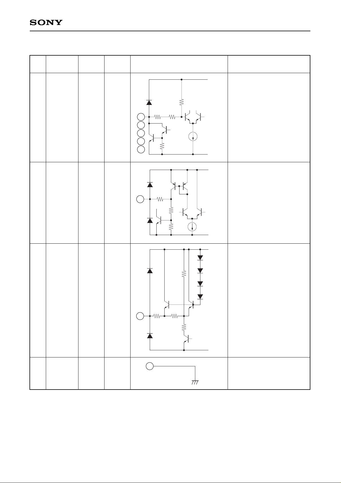
Pin Description
Pin
No.
1
2
3
19
20
FLAT
POP
ROCK
JAZZ
VOCAL
Mode selection input pins with
LED driving capability.
Flat initialization pin.
If the pin is connected to a
220nF capacitors, it initializes
to FLAT mode.
If the pin is not connected, it
initializes to ROCK mode.
Timing capacitor pin.
It is connected to a capacitor.
The charging and discharging
of this capacitor will determine
the timing of the logic control.
GND pin.
VCC or
1V
—
—
—
—
VCC –
5∗VBE
GND
FLAT
INIT
TIMING
CAP
GND
4
5
6
Symbol Voltage
I/O
resistance
Equivalent circuit Description
2
3
19
20
1
147 50k
50k
20k
GND
V
CC
GND
V
CC
147
20k
20k
4
5
GND
V
CC
147 150k
20k
100k
6
GND
Page 4
– 4 –
CXA2513M
Pin
No.
714IN1
IN2
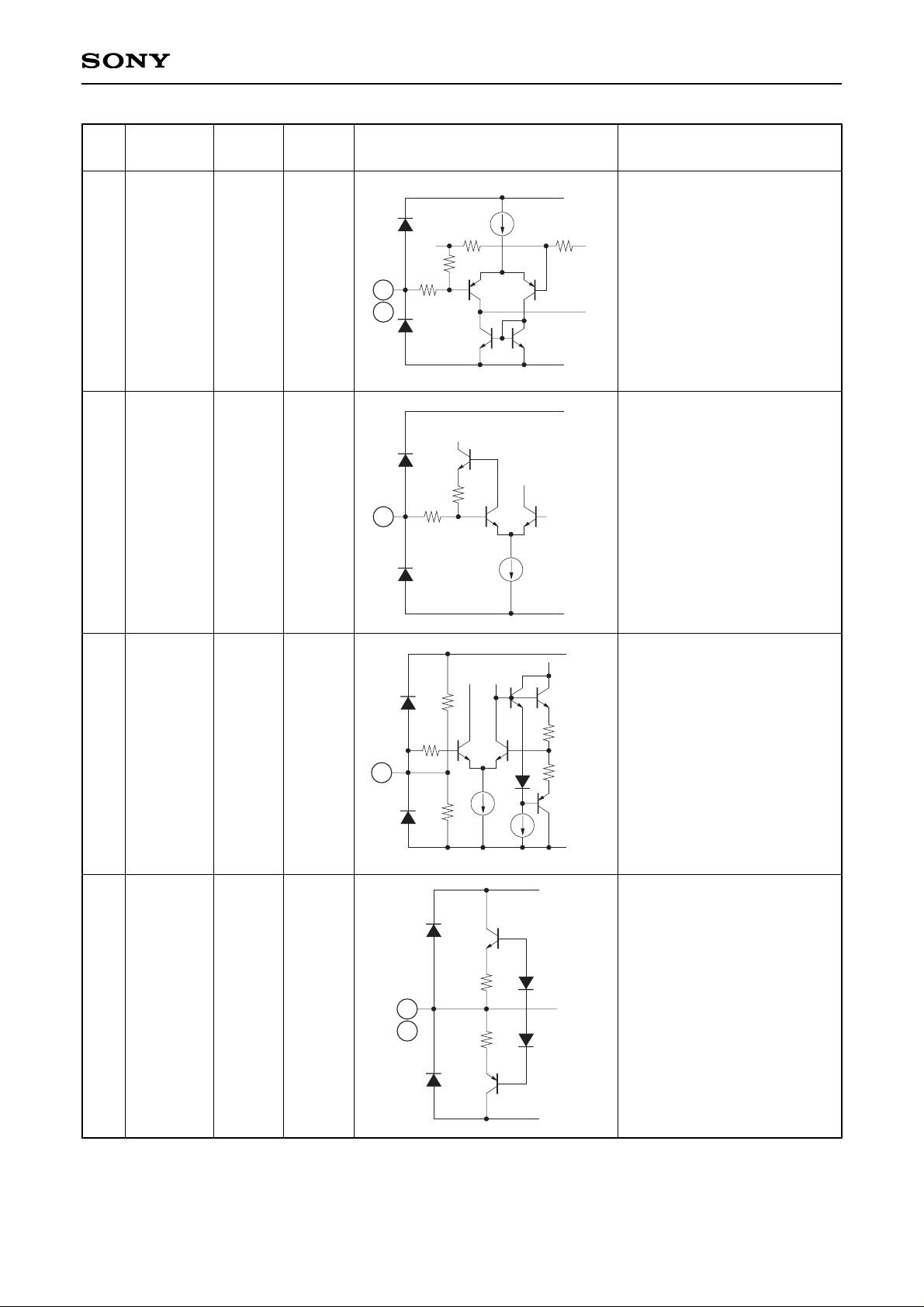
Signal input pin.
VCC/2
50k
Symbol Voltage
I/O
resistance
Equivalent circuit Description
7
14
GND
V
CC
50k
147
5k 11.5k
8 ISET
Reference current setting pin
(for graphic equalizer).
Normally 160kΩ resistor is
connected.
1.2V —
GND
V
CC
147
300
8
9 REF
Signal reference voltage pin.
A capacitor is connected for
ripple rejection.
VCC/2 40k
GND
V
CC
9
147
80k
80k
300
300
1011OUT1
OUT2
Signal output pin.
VCC/2 0
11
GND
V
CC
10
300
300
NPN
Page 5
– 5 –
CXA2513M
Pin
No.
17
MUTE
DET–
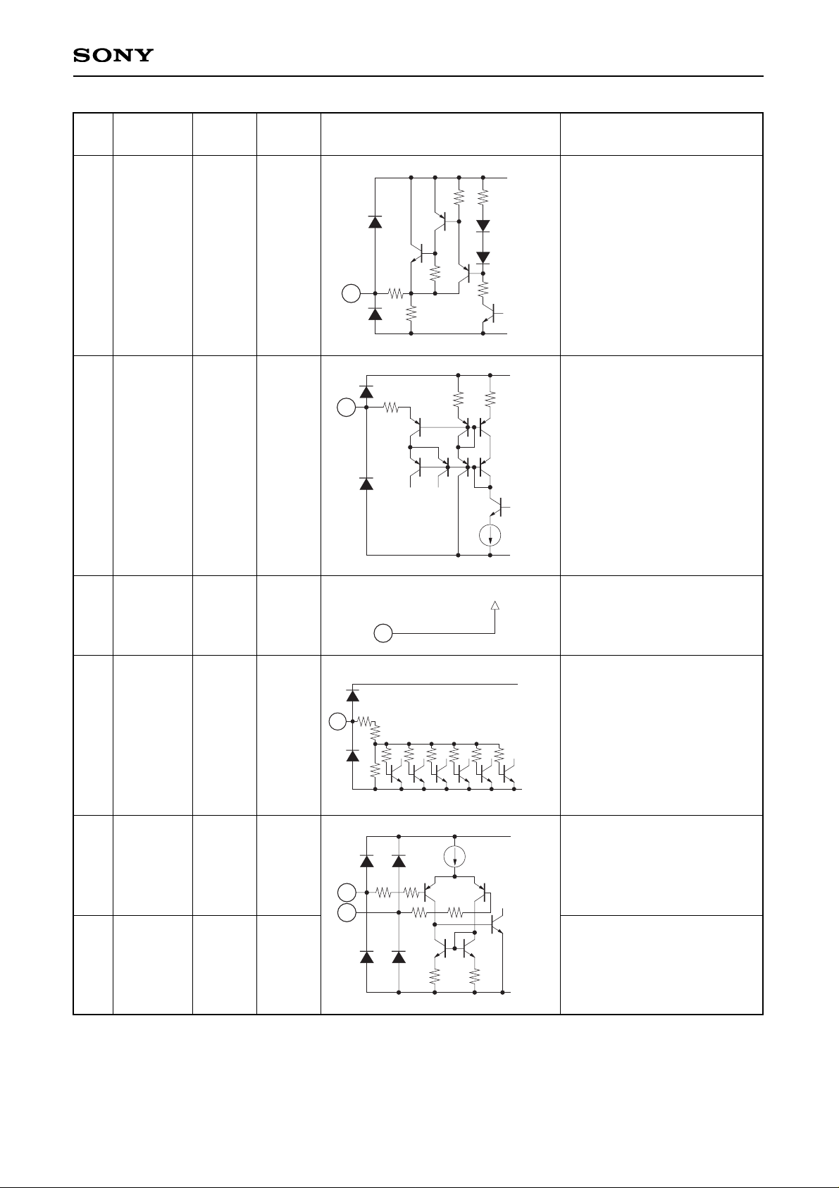
Negative input of the mute
detector comparator.
Positive input of the mute
detector comparator.
—
—
18
MUTE
DET+
—
—
Symbol Voltage
I/O
resistance
Equivalent circuit Description
GND
V
CC
17
4k4k
10k
147
10k147
18
13
LOW
FREQ
Low frequency adjustment pin.
Set the center frequency of
the bass.
VCC 0
GND
V
CC
147
10k 7.5k
13
12
MUTE
Mute pulse output pin.
0 300k
GND
V
CC
15k
40k
40k
300k
12
40k
147
15 VCC Power supply pin.VCC —
15
V
CC
16
STAND
BY
Standby pin.
When not connected, the IC in
standby.
When connected to VCC, the
IC in normal operation
— 20k
GND
V
CC
16
147
20k
50k
5k 5k 5k 5k 5k 5k
Page 6
– 6 –
CXA2513M
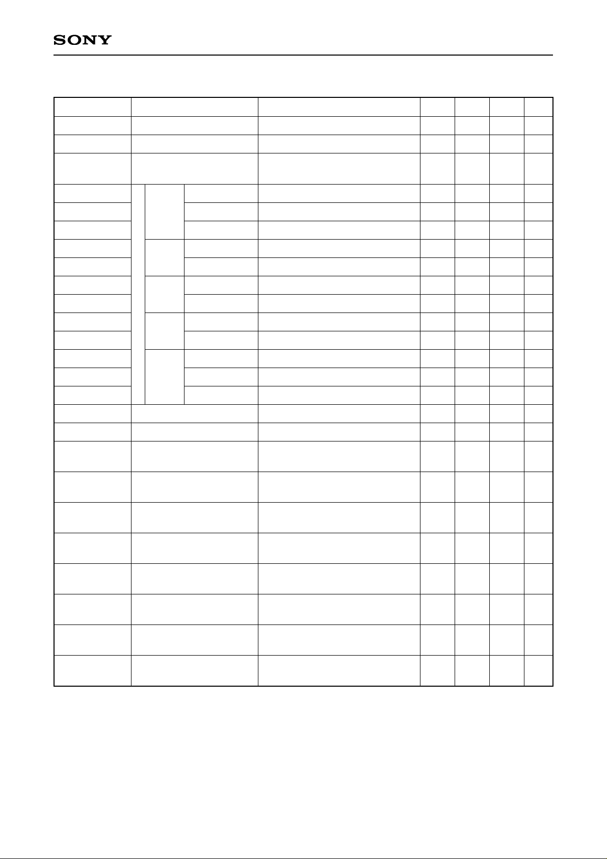
Electrical Characteristics (Ta = 27°C, VCC = 8V, C = 22µF)
Symbol
ICC (STANDBY)
ICC (FLAT)
Vout (max.)
GE (FLAT) B
GE (FLAT) M
GE (FLAT) T
GE (POP) M
GE (POP) T
GE (ROCK) B
GE (ROCK) T
GE (VOCAL) B
GE (VOCAL) M
GE (JAZZ) B
GE (JAZZ) M
GE (JAZZ) T
Bal
∆fO
THD
VNOIS (FLAT)
CS
PSRR
ILED
Vmute (off)
Vmute (on)
Vstandby (off)
Current consumption
Current consumption
Maximum output level
Balance
Center frequency deviation
Total harmonic distortion
Noise level
Channel separation
Power supply ripple
rejection
Maximum LED drive
current
Mute off voltage
Mute on voltage
Standby off voltage
Standby pin is low - No input
FLAT mode - No input
FLAT preset mode, f = 1kHz @
THD = 1%, RL = 10kΩ
Vin = 0.05Vrms, fO = 100Hz
Vin = 0.05Vrms, fO = 1kHz
Vin = 0.05Vrms, fO = 10kHz
Vin = 0.05Vrms, fO = 0.8 to 1.2kHz
Vin = 0.05Vrms, fO = 0.8 to 12kHz
Vin = 0.05Vrms, fO = 0.8 to 120Hz
Vin = 0.05Vrms, fO = 0.8 to 12kHz
Vin = 0.05Vrms, fO = 0.8 to 120Hz
Vin = 0.05Vrms, fO = 0.8 to 1.2kHz
Vin = 0.05Vrms, fO = 0.8 to 120Hz
Vin = 0.05Vrms, fO = 0.8 to 1.2kHz
Vin = 0.05Vrms, fO = 0.8 to 12kHz
GE (Out1) – GE (Out2)
RL = 10kΩ, FLAT preset mode,
f = 1kHz, Vin = 0.1Vrms
RL = 10kΩ, FLAT preset mode,
DIN AUDIO filter, Vin = 0Vrms
Vin = 0.1Vrms at 1kHz,
FLAT preset mode
Vin = 0.1Vrms at 100Hz,
FLAT preset mode
Current flowing through LED
connected to a switch depressed
Vm_det+ = 1/4VCC and
Vm_det– = 1/2VCC
Vm_det+ = 3/4VCC and
Vm_det– = 1/2VCC
ICC goes from standing to normal
operation
—
—
2.7
12.6
12.55
12.5
16.5
18.0
21.0
20.0
14.5
20.0
16.2
15.5
5.5
–1
–20
—
—
40
40
15
—
6.8
3
17.5
9.6
3.0
14.6
14.55
14.5
19.0
21.0
24.0
23.0
17.0
23.0
18.7
18.0
8.0
0
0
0.25
19
47
46
—
0
7.1
—
45.0
14.0
—
16.6
16.55
16.5
21.5
24.0
27.0
26.0
19.5
26.0
21.2
20.5
10.5
1
20
1
55
—
—
—
0.1
—
—
µA
mA
Vpeak
dB
dB
dB
dB
dB
dB
dB
dB
dB
dB
dB
dB
dB
%
%
µVrms
dB
dB
mA
V
V
V
Parameter Measurement conditions Min. Typ. Max. Unit
PRESETS
Normal
Bass
Mid
Treble
Mid Boost
Treble Boost
Bass Boost
Treble Boost
Bass Boost
Mid Boost
Bass Boost
Mid Boost
Treble Cut
POP
ROCK
VOCAL
JAZZ
Page 7
– 7 –
CXA2513M
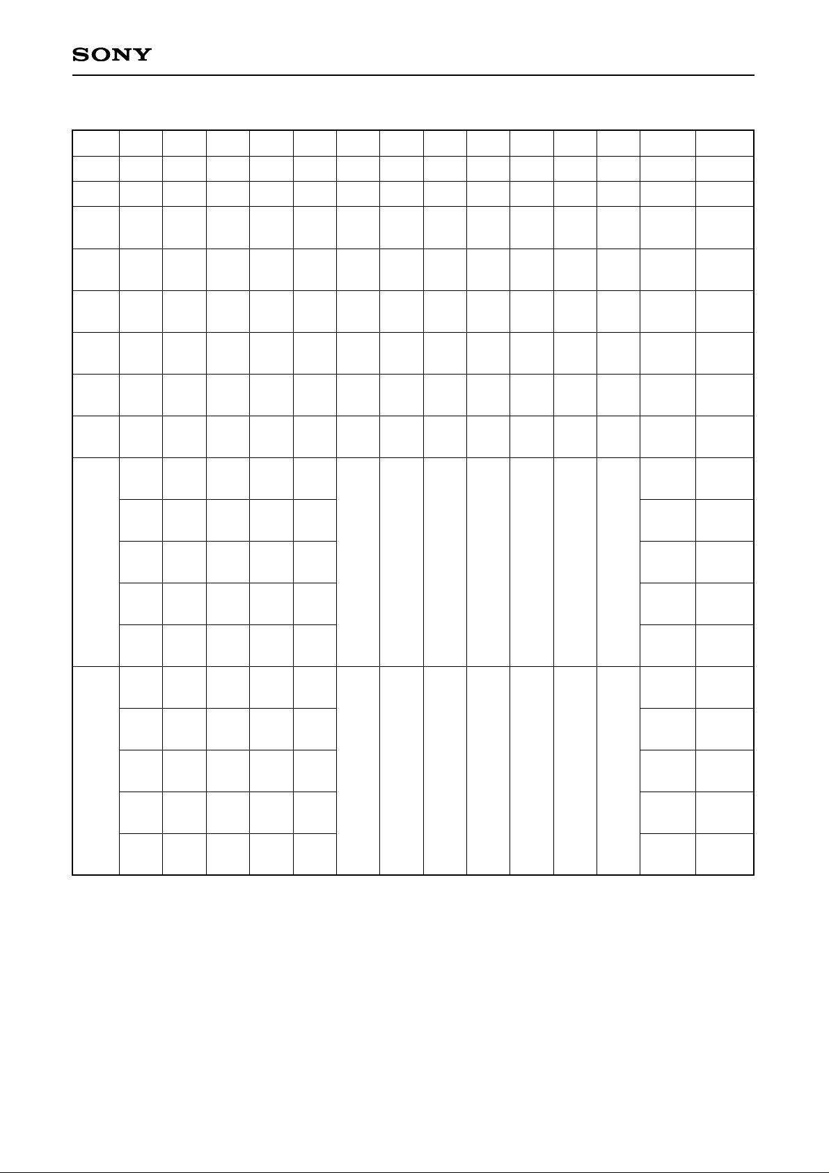
Switches Statuses
Item
1
2
3
4
5
6
7
8
—
•
•
•
—
—
—
—
•
—
—
—
—
•
—
—
—
—
—
—
—
—
•
—
—
—
—
•
—
—
—
—
•
—
—
—
—
—
—
—
—
•
—
—
—
—
•
—
—
—
—
•
—
—
—
—
—
—
—
—
•
—
—
—
—
•
—
—
—
—
•
—
—
—
—
—
—
—
—
•
—
—
—
—
•
—
—
—
—
•
•
•
•
•
•
•
•
•
•
•
•
•
•
•
•
•
3
2
2
2
2
2
2
2
off
off
on
on
on
on
on
on
•
•
•
•
•
•
•
•
on
on
on
on
on
on
on
on
off
off
off
off
off
off
off
off
—
—
V3
V4
V3
V4
V3
V4
V3
V4
V3
V4
V3
V4
V3
V4
V3
V4
V3
V4
V3
V4
V3
V4
V3
V4
V3
V4
V3
V4
V3
V4
V3
V4
ICC
ICC
Out1
Out2
Out1
Out2
Out1
Out2
Out1
Out2
Out1
Out2
Out1
Out2
Out1
Out2
Out1
Out2
Out1
Out2
Out1
Out2
Out1
Out2
Out1
Out2
Out1
Out2
Out1
Out2
Out1
Out2
Out1
Out2
S1 S2 S3 S4 S5 S6 S7 S8 S9 S10 S11 S12
Input pins
Test Pt.
•
•
•
•
2
2
on
on
•
•
ononoff
off
9
10
Page 8

– 8 –
CXA2513M
Item
11
12
13
14
15
16
17
18
•
•
•
•
•
•
•
•
—
—
—
—
—
—
—
—
—
—
—
—
—
—
—
—
—
—
—
—
—
—
—
—
—
—
—
—
—
—
—
—
•
•
•
•
O
•
•
•
•
•
•
•
•
•
O
•
2
2
2
2
2
2
2
3
on
on
on
on
on
on
on
on
•
•
•
O
•
•
•
•
on
on
on
off
on
on
on
on
off
off
off
off
off
off
off
off
V3
V4
V3 = 0
V4 = 0
V4
V3
V5
V5
—
—
—
V2
Out1
Out2
Out1
Out2
Out1
Out2
Out1
Out2
—
Mute
Mute
ICC
S1 S2 S3 S4 S5 S6 S7 S8 S9 S10 S11 S12
Input pins
Test Pt.
Page 9
– 9 –
CXA2513M
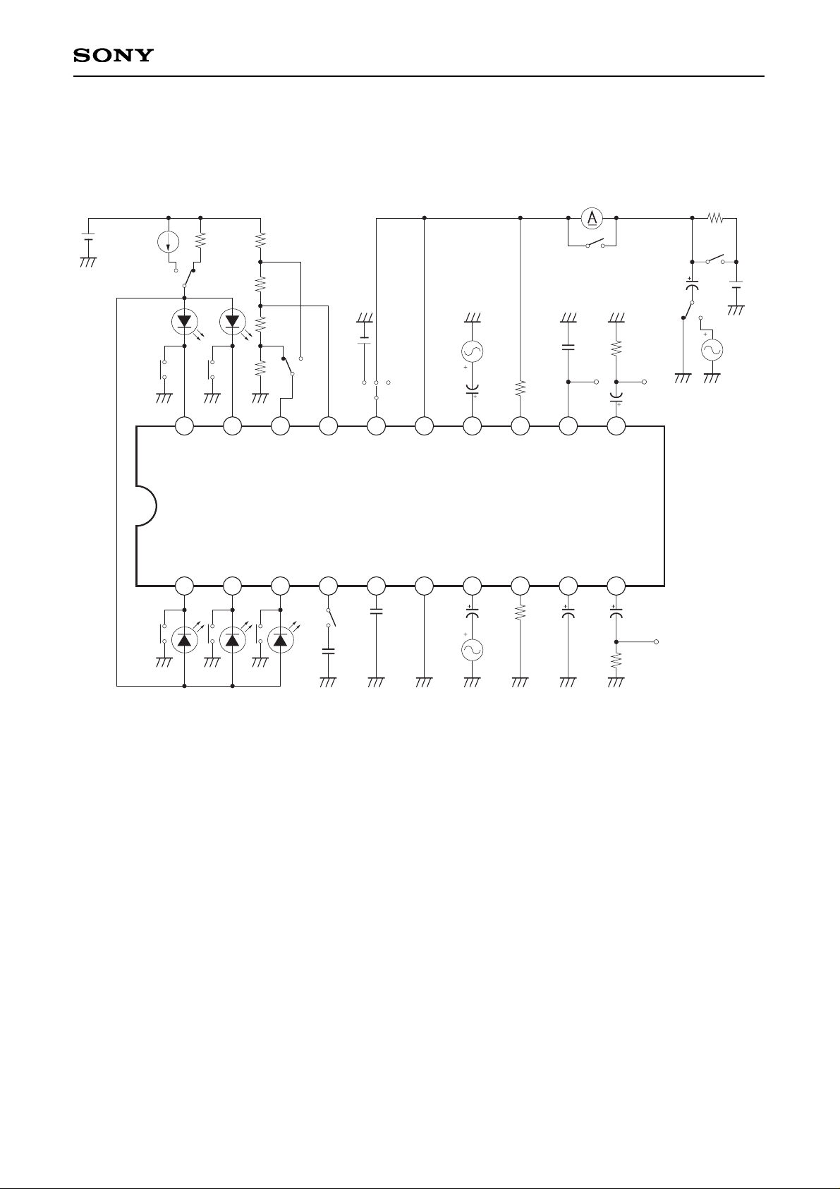
Electrical Characteristics Measurement Circuit
OUT2
GND
GND GND GND
C5
22µF
2
3
4
5
6
7
8
9
10
11
12
13
14
15
16
17
18
19
20
VOCALFLAT
JAZZPOP
M_DET+ROCK
M_DET–F_INIT
STANDBYT_CAP
V
CC
GND
IN2IN1
L_FREQISET
MUTEREF
OUT2OUT1
S2
D1
GND
S1
D3
GND
S3
D5
GND
GND
OUT1
R8
10k
C7
10µF
GND
R6
160k
GND
C3
10µF
V3
AC
C2
100nF
GND
C1
220nF
S12
GND
R1
470
MUTE
ICC
GND
I1
15µA
V1
8V
GND
R5
33k
R4
33k
R3
33k
GND
S7
R2
33k
S4
D4
S5
D2
GND
V2
3V
1 2 3
S8
GND
V4
AC
C4
10µF
R7
33k
GND
C6
3.3nFR910k
C8
10µF
S9
S11
R10
47
C9
470µF
V6
8V
GND
GND
V5
AC
GND
S10
S6
1
Page 10

– 10 –
CXA2513M
Application Circuit
OUT2
GND GND GND
C8
22µF
2
3
4
5
6
7
8
9
10
11
12
13
14
15
16
17
18
19
20
VOCALFLAT
JAZZPOP
M_DET+ROCK
M_DET–F_INIT
STANDBYT_CAP
V
CC
GND
IN2IN1
L_FREQISET
MUTEREF
OUT2OUT1
S2
D1
GND
S1
D3
GND
S3
D5
GND
OUT1
C10
10µF
GND
R5
160k
C2
220nF
GND
C3
100nF
To MUTE pin of
POWER AMPLIFIER
V
CC
GND
S6
S4
D4
S5
D2
GND
C7
10µF
R6
33k
GND
C9
3.3nF
R1
18k
C11
10µF
IN2VCC
GNDGND
C5
100nF
C4
470µF
VCC
C
C1
GND
R2
180
R3
22k
R4
180
∗
C6
10µF
IN1
∗ OPTIONAL CAPACITOR
no capacitor – ROCK MODE
1
Application circuits shown are typical examples illustrating the operation of the devices. Sony cannot assume responsibility for
any problems arising out of the use of these circuits or for any infringement of third party patent and other right due to same.
Page 11
– 11 –
CXA2513M
Description of Operation
1. Graphic Equalizer
• Conventional system
BOOSTCUT-OFF
R2
Vo
Operational amplifier
R
1
VI
RO = R1 = R2
RV
L
C
R
Z (s)
Fig. 1
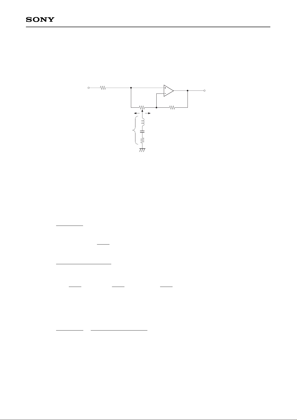
Fig. 1 indicates the conventional graphic equalizer system. This circuit performs boost and cut-off near "fO"
controlled by the potentiometer Rv. ("fO" is resonance frequency determined by Z (s) (formed LCR).) The
operation can be seen as follows: When the LCR circuit goes to the far left of Rv, a state of graphic equalizer
becomes maximum cut-off. At that time, assuming transmittance as T (s), the following expression can be
obtained.
T (s) =
Z (s) + Ro
Z (s)
T (s) = =
Z (s)
Z (s) + RO
LCS2+ RCS + 1
LCS2+ (R + RO) Cs + 1
LCS2+ (R + RO) CS + 1
LCS2+ RCS + 1
Here as
Z (s) = sL + R +
sC
1
Defining fO as fO =
, ωo as ωo =
2π
ωo
LC
1
, and Q as Q =
, the frequency response can be obtained
at cut-off
R
ωoL
Also, when LCR circuit goes to the far right of Rv, a state of graphic equalizer becomes maximum boost. At
that time transmittance is:
Defining fO, ωo and Q as for cut-off the frequency response can be obtained at boost.
Then T (s) =
Page 12

– 12 –
CXA2513M
Fig. 2 indicates frequency response at boost and cut-off.
Frequency [Hz]
Response [dB]
0dB
f
O
Boost
Flat
Cut-off
f
O =
1
2π √ LC
Fig. 2
• CXA2513M system
IbIc
Gm2Gm1
R
Vo
Operational amplifier
Z (s)
Z (s)
H (s)
R
V
I
H (s) =
ωo
Q
s
ωo
Q
s
2
+ s + ωo
2
Fig. 3
The structure of the graphic equalizer used in this IC is shown on Fig. 3. This circuit performs boost and cut-off
controlled by 2 transconductance amplifiers that can vary the conversion coefficient through control currents Ib,
and Ic around ωo. ("ωo" is center frequency determined by band-pass filter.) Output impedance Z (s) of Gm1,
Gm2 can be expressed as
T (s) =
H (s) · Gm1
1
Page 13
– 13 –
CXA2513M
Here, using ωo and Q BPF transmittance H (s) is expressed as
H (s) =
ωo
Q
ωo
H (s) = s + +
ωo · Gm1
Q
Gm1
1
Gm1 · s
ωo · Q
Q
+ ωo
2
S2+
s
T (s) = =
(1 + R · Gm) · ωo
2
Q
ωo
Z (s) + R
Z (s)
Q
· s + ωo
2
S2+
S2+
· s + ωo
2
T (s) = =
(1 + R · Gm) · ωo
2
Q
ωo
Z (s)
Z (s) + R
Q
· s + ωo
2
S2+
S2+
· s + ωo
2
The formula shows that this system and the aforementioned LCR circuit have equivalent impedance
characteristics on Z (s).
Then, regarding Gm as the maximum value of Gm1 and Gm2, the operation can be observed as follows.
Maximum cut-off occurs when Gm1 = Gm and Gm2 = 0. At that time transmittance T (s) is expressed as
This is equal to the frequency response of the conventional graphic equalizer at cut-off.
Also, maximum boost occurs when Gm1 = 0 and Gm2 = Gm. At that time transmittance T (s) is given by as
This is equal to the frequency response of the conventional graphic equalizer at boost.
As far as the operation is concerned the graphic equalizer on this IC and the conventional graphic equalizer
are equal, even when the system differs. The merit in using this IC's system rests with the fact that monolithic
filter technology realizes a graphic equalizer without external parts.
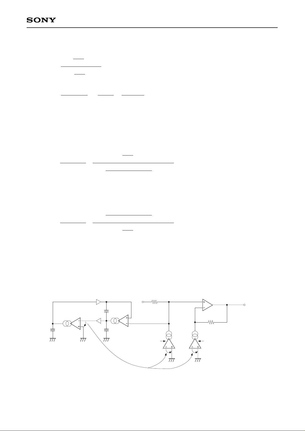
The structure of the actual graphic equalizer, including BPF, is shown on Fig. 4.
I BOOSTI CUT-OFF
Gm4Gm3
R2
30k
Vo
SUM
V
I
R1
30k
GNDGND
C3
C1
GND
1
1
GND
Gm2
C2
GND
V1
Gm1
Fig. 4
Page 14
– 14 –
CXA2513M
2. Power Up
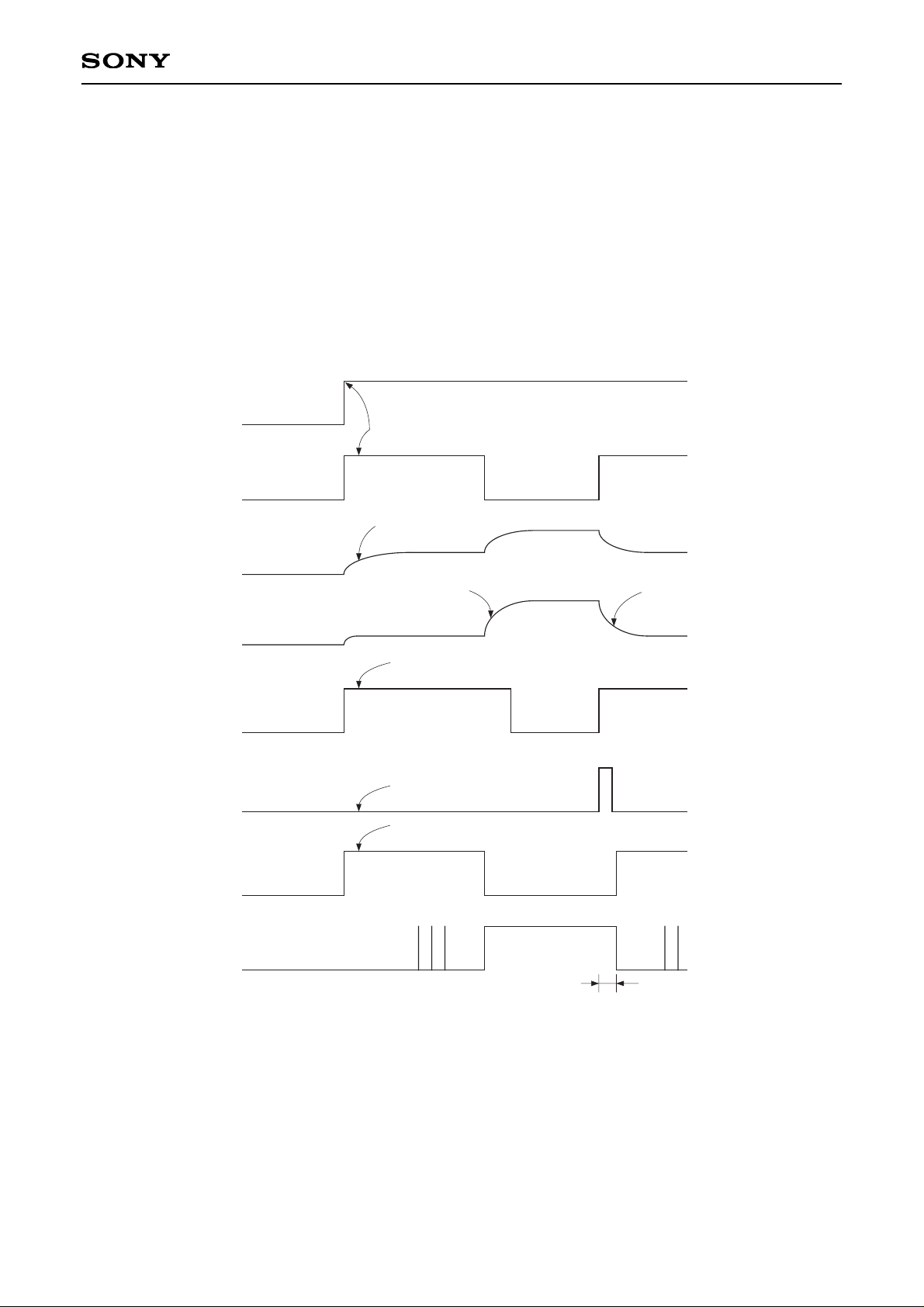
There are two ways of powering up the CXA2513M. They are
1) VCC pin (Pin 15) goes high, and after some time, the STANDBY pin (Pin 16) goes high.
2) VCC pin and STANDBY pins both goes high together.
The two ways of power-up will results in different timing diagram and different initial mode.
If both VCC and STANDBY pins go high together, the REF capacitor (Pin 9) will charge to half VCC. The IC will
be initialized to ROCK mode. The timing diagram is shown in Fig. 5.
VCC pin
STANDBY pins
REF pin
TIMING CAP pin
ISET pin
LATCH
OUTPUT
ENABLE
LATCH
ENABLE
MUTE pin
t2
Only ROCK mode initialized
Latch output disable
Bandgap voltage present
Charge to V
CC
Discharge to clamped voltage
Charge to 0.5V
CC
Turn on at the same time
Fig. 5
Page 15
– 15 –
CXA2513M
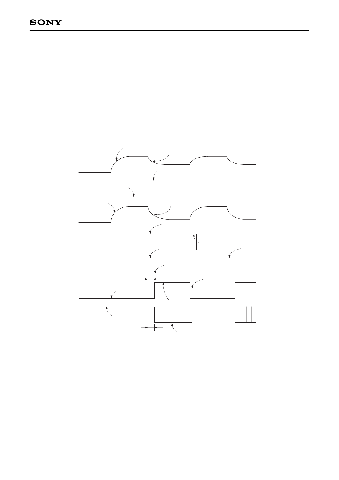
If the VCC pin goes high while the STANDBY pin is not connected to VCC, the IC is in standby condition. The
REF capacitor (Pin 9) and timing capacitor (Pin 5) will charge to VCC. Now, if the STANDBY pin is switched to
VCC, the REF capacitor will discharge to half VCC and the timing capacitor will discharge to a clamped voltage
(VCC – 5∗VBE).
During the discharging of timing capacitor, all the LEDs light up. When the timing capacitor voltage reaches a
certain threshold voltage, only the ROCK LED or FLAT LED lights up depending on Pin 4. If the Pin 4 is
connected to a capacitor, the IC is initialized to FLAT mode. If the Pin 4 is not connected, the IC is initialized to
ROCK mode. The timing diagram is shown in Fig. 6.
VCC pin
STANDBY pins
REF pin
TIMING CAP pin
ISET pin
LATCH
OUTPUT
ENABLE
LATCH
ENABLE
MUTE pin
t2
Latch disable
AII LEDs light up
Bandgap voltage present
Charge to V
CC
Charge to VCC
Normal operation
Discharge to 0.5VCC
Normal operation
Store the present mode
Latch through what depressed mode
Mute On
t1
Latch on the initial mode
Restore the previous mode
Standby on
Discharge to clamped voltage
Delay the
shutdown
Fig. 6
Page 16

– 16 –
CXA2513M
3. Mute Pulse Generation
The CXA2513M has one voltage comparator built-in. The built-in voltage comparator is used to produce mute
pulse during the depress of the preset mode switches. During depress the switch, there is a voltage pulse of
about 1V depending appearing at the cathode of the LEDs.
The mute detector comparator is used to detect this voltage changes at the cathode of LEDs and produce
mute pulse at Pin 12. The polarity of the mute pulse can be set. When the M_DET+ pin (Pin 18) is higher than
the M_DET– pin (Pin 17), the MUTE pin (Pin 12) will be high. When the M_DET+ pin (Pin 18) is lower than the
M_DET– pin (Pin 17), the MUTE pin (Pin 12) becomes low.
A capacitor is used to store the initial voltage before the depression of the mode switch. Once the switch is
depressed, the capacitor starts discharge. The values of the resistors and capacitor set the duration of the
mute pulse.
Notes on Operation
1) Value of Timing Capacitor
The timing and the duration of the MUTE pin and the LEDs light-up depends on the value of the timing
capacitor as the timing capacitor is discharging to (VCC – 5∗VBE).
The charging time constant is 250K∗(timing capacitor) and the discharging time constant is 150K∗(timing capacitor).
The two threshold values: a) Latch Output Enable (LATCH_OE_ctl)
b) Latch enable/Mute disable (LATCH_ctl)
The threshold values of the Latch Output Enable (LATCH_OE_ctl) is set to (VCC – 3∗VBE) and the threshold
values of the Latch enable/Mute disable (LATCH_ctl) is set to (VCC – 4∗VBE).
So, the duration for all the LEDs light-up is
2∗VBE = (5VBE) exp (–t1/RC)
where R = 150K
and the sound appears after t2 seconds if the mute pulse output pin is used. This t2 is given by
VBE = (5VBE) exp (–t2/RC)
where R = 150K
Therefore, depending on the requirements of the time on the mute sound and the duration of all LEDs light-up,
choose the value of the timing capacitors.
Page 17
– 17 –
CXA2513M
2) Initialize Preset IC
The preset IC can be initialized into any one of the two modes out of the total 5 mods. The two modes are:
a) FLAT
b) ROCK
In order to initialize the preset IC into FLAT, one external capacitor (220nF) is required. While to initialize the
preset IC to ROCK, no external capacitor is required.
3) Supply voltage Ripple Rejection
The value of the REF capacitor (Pin 9) determines the supply voltage ripple rejection ratio (SVRR). A reduce in
this capacitance value decreases on the supply voltage ripple rejection ratio (SVRR).
4) Center Frequency of Band-pass Filters
The center frequency of the graphic equalizer is determined by an external resistor. This resistor is 160kΩ
external resistor connected to the ISET pin (Pin 8). It is recommended to use a resistor with the small
dispersion and temperature coefficients.
By varying the value of the resistor connected to the ISET pin, the frequency response of the graphic equalizer
can be shifted. By reducing the resistor value, all the three band-pass filters shift to high band. By increasing
the resistor value, the filters shift to lower band.
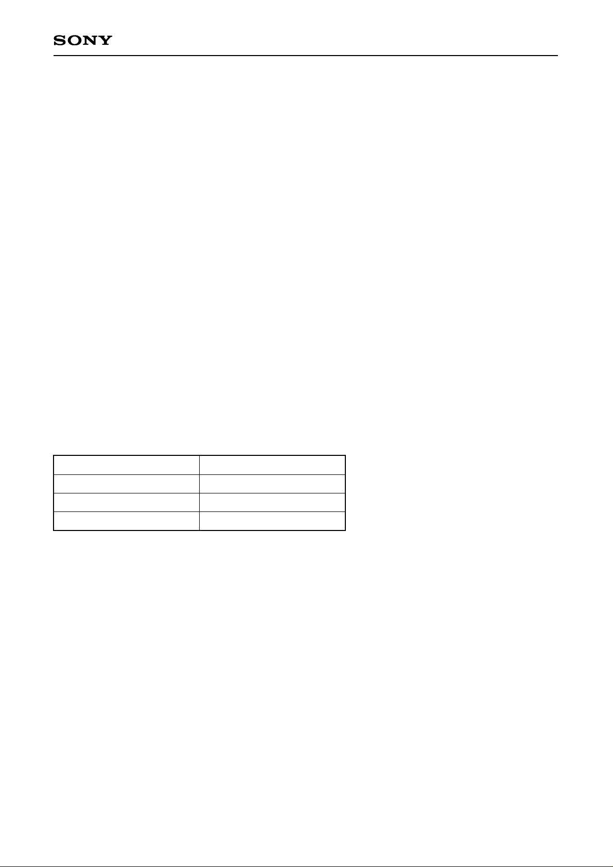
The center frequency of the bass band-pass filter can be varied independently. This bass center frequency is
determined by the external resistor (33kΩ) connected to the LOW-FREQ pin (Pin 13). By reducing the value of
this resistor, the bass center frequency shifts to higher frequency. By this value, the bass center frequency
shifts to lower frequency.
LOW-FREQ resistor
56kΩ
33kΩ
10kΩ
70Hz
100Hz
200Hz
Bass center frequency
Page 18
– 18 –
CXA2513M
Example of Representative Characteristics
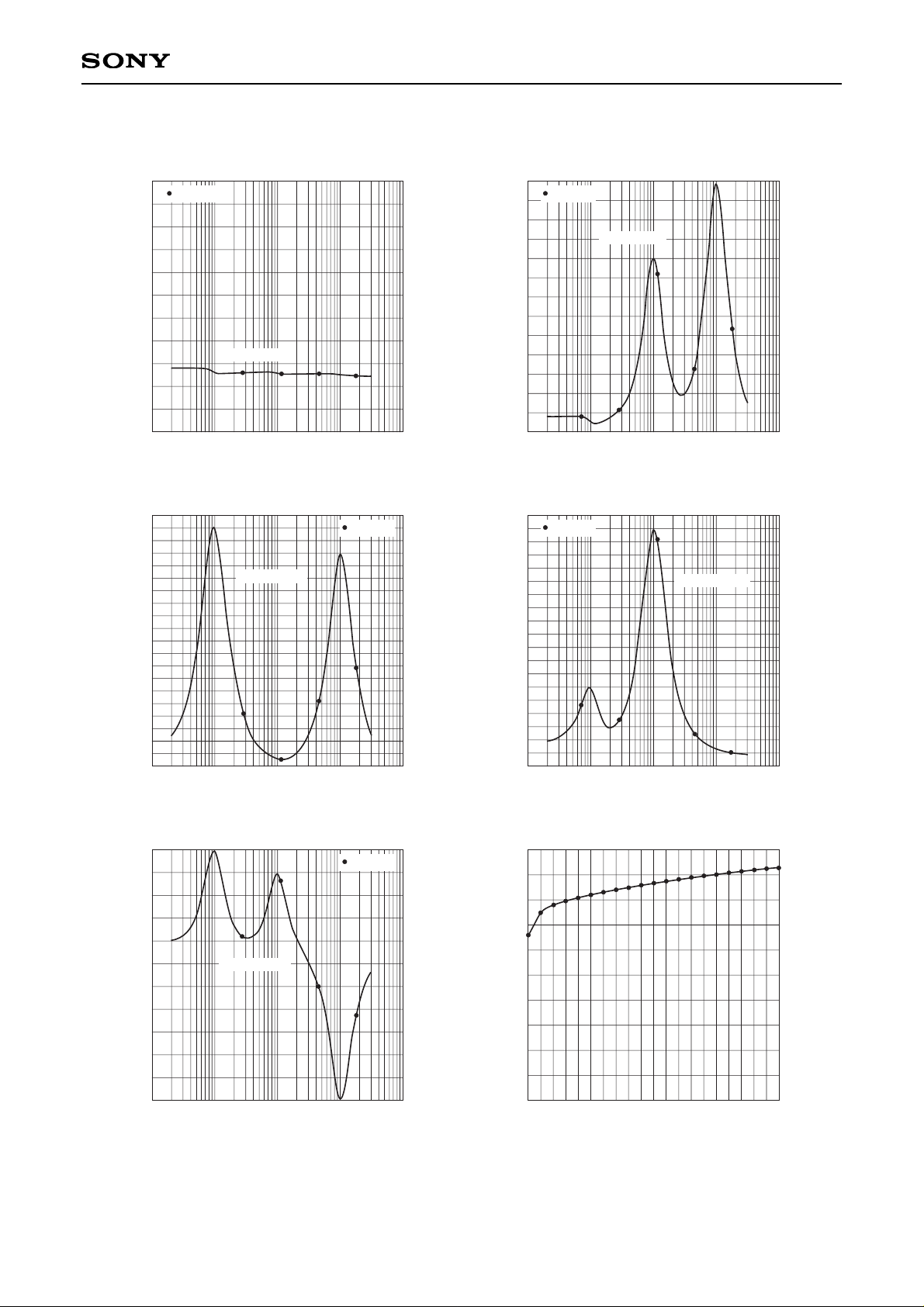
AC response
a) Frequency response of FLAT mode
10
1
10
2
10
3
10
4
10
5
23
22
21
20
19
18
17
16
15
14
13
12
FLAT MODE
[freq]
: Output
10
1
10
2
10
3
10
4
10
5
21.0
20.5
19.5
18.5
18.0
17.5
17.0
16.5
16.0
15.5
15.0
14.5
POP MODE
20.0
19.0
AC response
b) Frequency response of POP mode
[freq]
: Output
10
1
10
2
10
3
10
4
10
5
23.5
22.5
20.5
18.5
18.0
17.5
17.0
16.5
16.0
15.5
15.0
14.0
VOCAL MODE
21.5
19.5
14.5
23.0
22.0
21.0
20.0
19.0
AC response
d) Frequency response of VOCAL mode
[freq]
: Output
10
1
10
2
10
3
10
4
10
5
24.5
23.5
22.5
21.5
20.5
19.5
18.5
17.5
16.5
15.5
15.0
14.5
ROCK MODE
24.0
23.0
22.0
21.0
20.0
19.0
18.0
17.0
16.0
AC response
c) Frequency response of ROCK mode
[freq]
: Output
10
1
10
2
10
3
10
4
10
5
19
18
17
16
15
14
13
12
11
10
9.0
8.0
JAZZ MODE
AC response
e) Frequency response of JAZZ mode
[freq]
: Output
0 5 10 15 20
1
0.9
0.8
0.7
0.6
0.5
0.4
0.3
0.2
0.1
0
1 6 11 162 7 12 173 8 13 184 9 14 19
LED current [mA]
LED driving voltage [V]
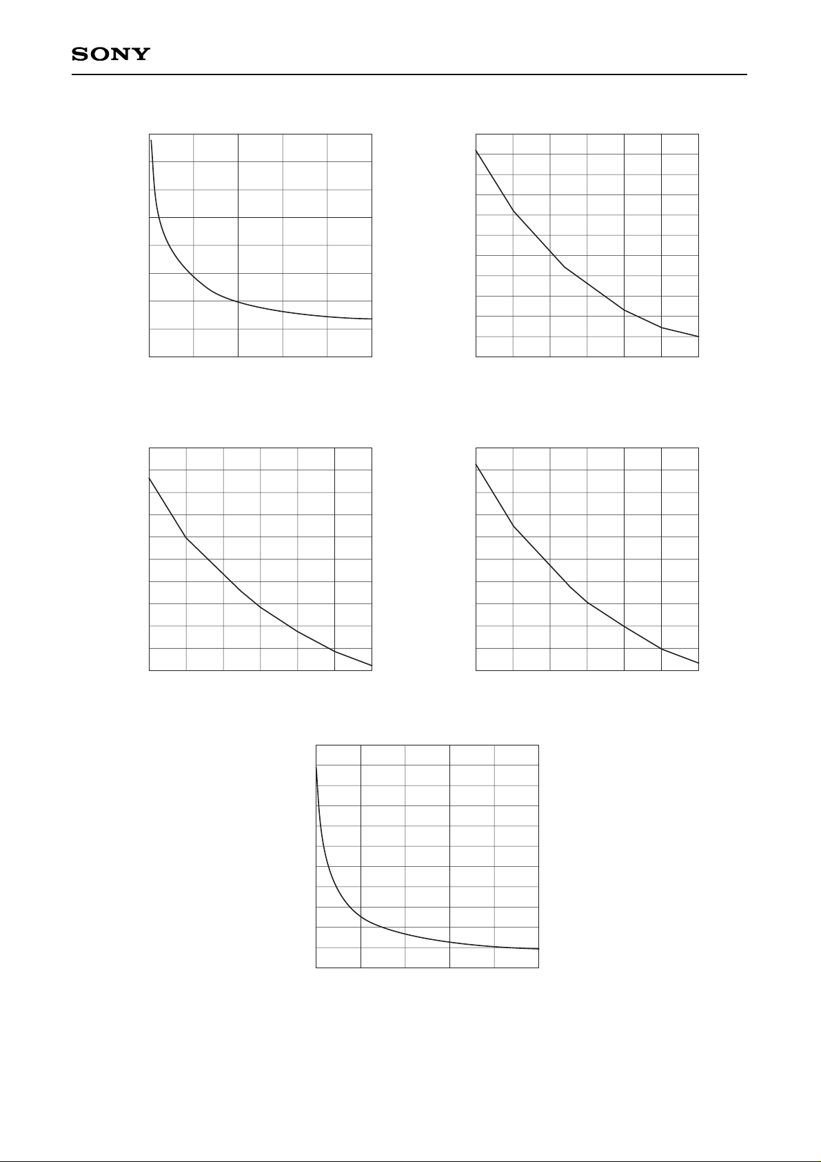
LED current vs. LED driving voltage
f) LED current vs. LED driving voltage
(Pins 1, 2, 3, 19 and 20)
Page 19
– 19 –
CXA2513M
0 20 40 60 80 100
Capacitance [µF]
–60
–55
–50
–45
–40
–35
–30
–25
–20
Ripple rejection @100Hz [dB]
Ripple rejection @100Hz vs. Capacitance
g) Ripple Rejection at 100Hz vs.
Reference Capacitor (FLAT MODE)
100 120 160 180 200 220
Resistance [kΩ]
60
70
80
90
100
110
120
130
140
Bass center frequency [kHz]
Bass center frequency vs. Resistance
h) Bass Center Frequency vs.
ISET Resistor (L-FREQ Resistor = 33kΩ)
140
150
160
100 120 160 180 200 220
Resistance [kΩ]
0.7
0.8
0.9
1
1.1
1.2
1.3
1.4
Mid center frequency [kHz]
Mid center frequency vs. Resistance
140
1.5
1.6
i) Mid Center Frequency vs. ISET Resistor
100 120 160 180 200 220
Resistance [kΩ]
7
8
9
10
11
12
13
14
Treble center frequency [kHz]
Treble center frequency vs. Resistance
140
15
16
j) Treble Center Frequency vs. ISET Resistor
17
0 40 60 80 100
Resistance [kΩ]
0
50
100
150
200
250
300
350
400
Bass center frequency [kHz]
Bass center frequency vs. Resistance
k) Bass Center Frequency vs.
L-FREQ Resistor (ISET Resistor = 160kΩ)
20
450
500
Page 20
– 20 –
CXA2513M
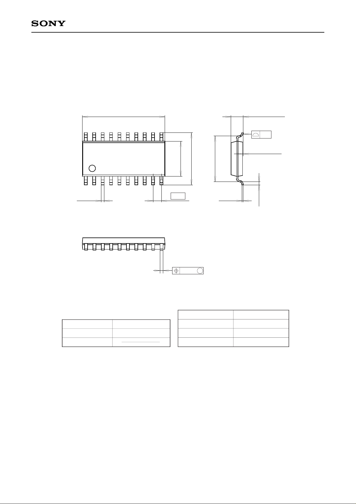
Package Outline Unit: mm
SONY CODE
EIAJ CODE
JEDEC CODE
SOP-20P-L01
SOP020-P-0300
PACKAGE STRUCTURE
PACKAGE MATERIAL
LEAD TREATMENT
LEAD MATERIAL
PACKAGE MASS
COPPER ALLOY
SOLDER PLATING
EPOXY RESIN
0.3g
20PIN SOP (PLASTIC)
12.45 – 0.1
+ 0.4
20
11
0.45 ± 0.1
1.27
10
1
5.3 – 0.1
+ 0.3
7.9 ± 0.4
6.9
0.2 – 0.05
+ 0.1
0.5 ± 0.2
0.1 – 0.05
+ 0.2
1.85 – 0.15
+ 0.4
0.15
0.24
M
 Loading...