

Page 1

– 1 –
Description
The CXA2002R is a bipolar IC developed as
recording/playback amplifiers for Hi8 VCRs.
Features
• Recording/playback system
• Wideband recording/playback amplifier for Hi8
VCR
• Supports electronic volume (EVR) control (3V)
• Recording system
• Recording amplifier feedback dumping circuit and
its EVR control function facilitates printed circuit
board design.
• Five-input (Y, chroma, AFM, ATF and PCM) mix
amplifier and EVR control function of Y and lowband recording level
• Ramp circuit for the recording amplifier output
bias current
• Playback system
• Playback amplifier feedback dumping circuit
facilitates printed circuit board design.
• Middle-band compensation circuit (middle tune)
and independent adjustments of the center
frequency, Q and boost by EVR
• RFAGC and dropout detection circuits
Absolute Maximum Ratings
• Supply voltage VCC 7V
•Operating temperature Topr –10 to +75 °C
• Storage temperature Tstg –65 to +150 °C
• Allowable power dissipation PD 1100 mW
(when mounted on the printed circuit board)
Recommended Operating Condition
• Supply voltage 4.75
+0.5
–0.25
V
• Vcc EVR voltage 3.15 ±0.15 V
CXA2002R
48 pin LQFP (Plastic)
E95201-ST
2-channel Recording/Playback Amplifier
Application
8 mm VCR
Structure
Bipolar silicon monolithic IC
Sony reserves the right to change products and specifications without prior notice. This information does not convey any license by
any implication or otherwise under any patents or other right. Application circuits shown, if any, are typical examples illustrating the
operation of the devices. Sony cannot assume responsibility for any problems arising out of the use of these circuits.
Page 2

CXA2002R
– 2 –
Block Diagram
HEAD
REC
V/I
RAMP
GEN
15dB
40dB
VPSW1
VPSW2
PCM
VIDEO
YGCA
1
1
1
1
1
1
2
CGCA
LOWGCA
LOWGCA
RF
AGC
AGCDET
DOCDET
M · T
–6dB
12dB
MUTE
2CH
1CH
MUTE
2CH
1CH
PCMSW
VIDEOSW
REC
HEAD
40dB
15dB
V/I
RAMP
GEN
RAMPCONT
RAMP
RFSWP
BOTH REC
RP PB
MTQ
MTF0
MTG
PCMOUT
MTOUT
40
39
38
37
41
42
43
44
45
46
47
48
2
3
4
5
6
7
8
9
10
11
12
1
13
1415
16
17
18
19
20
21
22
23
24
25
26
27
28
29
30
36
35
34
31
32
33
VPPCMIN
RECPCM
VPVTRIN
RECVIDEO
VREG
GND
IR1
IR
VG2
PCMIN
PCMREC
ATFIN
CCONT
AFMIN
AFREC
CIN
LOWLEVEL
YIN
YLEVEL
RFAGCOUT
RFAGCTC
RFAGCIN
DOCDET
DOP
V
CC2
REC2CONT
REC2OUT
PB2IN
PBDUMP2
PBDUMP1
GND1
PB1IN
REC1OUT
REC1CONT
V
CC1
GND2
V
CC
V
CC
EVR
PCM
VIDEO
Page 3

CXA2002R
– 3 –
Pin Description
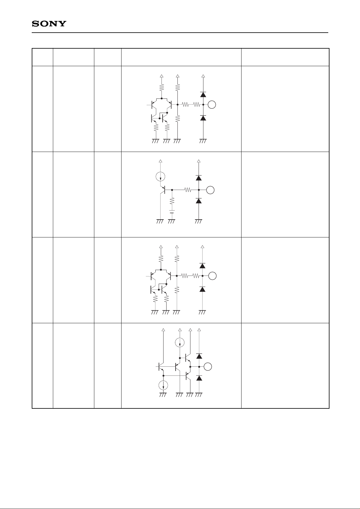
1 CCONT —
EVR adjusting pin for the
recording chroma level.
Increasing the applied voltage
reduces the gain.
2 AFMIN —
Input pin for recording AFM.
DC component is cut by
built-in C.
Input level: 125mVp-p (typ.)
3 AFREC —
After-recording mode
switchover pin (High: Afterrecording)
H: 2.3V or above
L: 0.6V or below
4 CIN 2.45
Recording chroma input pin.
Input after cutting DC
component with C.
Input level: 300mVp-p (typ.)
1
14350k
10k25k
15k
7k
7k
2
143
20p
70µ
50k
143
35µ
3
35µ35µ
1.5V
143
2.45V
70µ
50k
4
Pin
No.
Symbol
Pin
voltage
Equivalent circuit Description
Page 4
CXA2002R
– 4 –
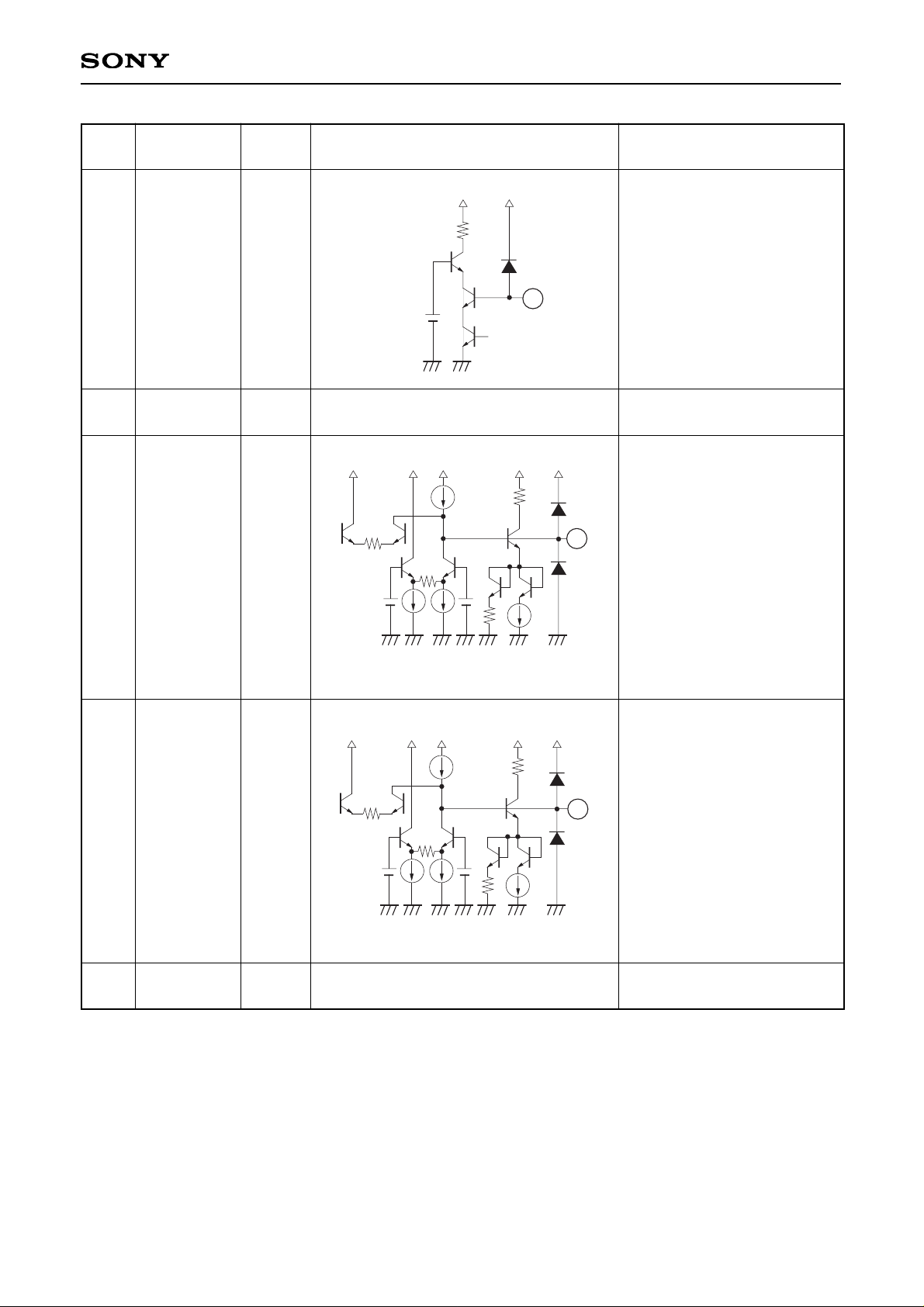
5 LOWLEVEL —
EVR adjusting pin for
recording RF.
Increasing the applied voltage
reduces the gain.
Simultaneous adjustment of
VIDEO and PCM paths.
VIDEO path: C+AFM+ATF
adjustment
PCM path: ATF adjustment
6 YIN 2.45
Recording Y input pin.
Input after cutting DC
component with C.
Input level: 500mVp-p (typ.)
7 YLEVEL —
EVR adjusting pin for the
recording Y signal level.
Increasing the applied voltage
reduces YLEV.
8 RFAGCOUT 2.8
Playback Y signal output pin.
Output level: 410mVp-p (typ.)
14350k
10k25k
15k
7k7k
5
143
40µ
50k
2.45V
6
14350k
10k25k
15k
7k7k
7
8
40µ
600µ
410µ
Pin
No.
Symbol
Pin
voltage
Equivalent circuit Description
Page 5

CXA2002R
– 5 –
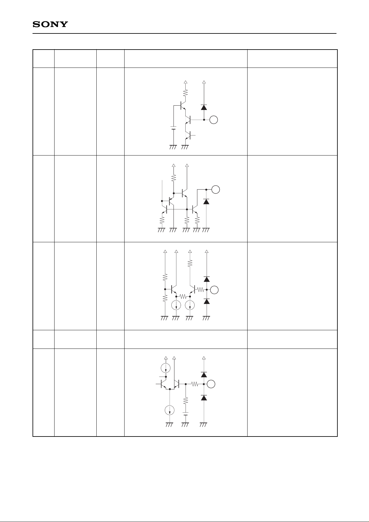
9
RFAGCTC —
Pin to apply time constant of
RFAGC.
EVR adjustment of RFAGC
gain is possible.
Adjustment range:
(
2.5V to 4.75V
)
Gain: Small to Large
10 RFAGCIN —
RFAGC input pin for the
playback Y signal.
Playback VIDEO signal output
to Pin 14 (MTOUT) is input
again to Pin 10 (RFAGCIN)
via external ATF TRAP, AFM
TRAP and C TRAP.
DC component is cut by
built-in C.
11 DOCDET 2.5
Pin to determine the dropout
detection level.
12 DOP
H: 3.15
L: 0
Output pin for the dropout
detection signal.
High upon dropout.
143
50µ50µ25µ25µ
9
143
50µ
50k
3.25V
10
13p
143
50µ
79k
11
47k
4.15V
12
150
2.4k
1.3m
3.15V
9
Vcc
4700p
470k
Pin
No.
Symbol
Pin
voltage
Equivalent circuit Description
Page 6

CXA2002R
– 6 –
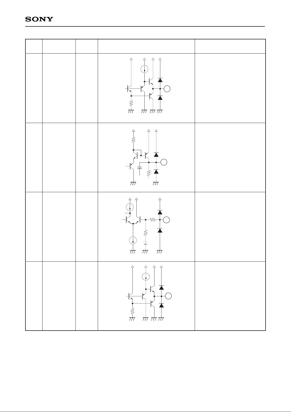
14 MTOUT 2.4
Output pin for playback
VIDEO signal.
Y + C + AMF + ATF is output.
13 VCC EVR 3.15
Power supply pin for EVR block.
15 MTG —
EVR adjusting pin for the
middle-tune boost.
Increasing the applied
voltage reduces the boost.
16 PCMOUT 2 Output pin for playback PCM
17 MTF0 —
EVR adjusting pin to
determine middle-tune fo.
Increasing the applied voltage
increases fo.
40µ
400µ
14
330µ
14350k
10k25k
15k
7k7k
15
40µ
360µ
16
3.5k
310µ
14350k
10k25k
15k
7k7k
17
Pin
No.
Symbol
Pin
voltage
Equivalent circuit Description
Page 7

CXA2002R
– 7 –
18
RP PB —
REC/PB switchover pin
High: PB 2.3V or above
Low: REC 0.6V or below
19 VCC 4.75
Power supply pin for
components other than REC
amplifier, PB amplifier and EVR.
20 BOTH REC —
EACH REC/BOTH REC
switchover pin.
High: BOTH REC 2.3V or
above
Low: EACH REC 0.6V or
below
21 RFSWP —
RFSWP input pin.
High: 2.3V or above
Low: 0.6V or below
22 RAMP —
Pin to turn ON/OFF the REC
amplifier bias current during
after-recording. The bias
current turns ON when this pin
goes high.
High: 2.3V or above
Low: 0.6V or below
18
50k
143
6.1k
35µ35µ35µ
1.5V
143
35µ
35µ
35µ
1.5V
20
143
35µ35µ35µ
1.5V
21
143
35µ35µ35µ
1.5V
22
Pin
No.
Symbol
Pin
voltage
Equivalent circuit Description
Page 8

CXA2002R
– 8 –
23 RAMPCONT —
Ramp pulse rising slope
switchover pin.
Low: 32µA/µs 0.6V or below
High: 17µA/µs 2.3V or above
(The fall time is 32µA/µs in
both cases.)
25 VCC1 4.75
Power supply pin for CH1 REC
amplifier and PB amplifier.
24 MTQ —
EVR adjusting pin to
determine middle-tune Q.
Increasing the applied
voltage increases Q.
26 REC1CONT —
EVR adjusting pin for the CH1
recording dumping level.
Reducing the applied voltage
strengthens dumping.
27 REC1OUT —
CH1 recording output pin.
Open collector.
143
35µ35µ35µ
1.5V
23
143
50k
10k25k
15k
7k7k
24
26
143
270
71k
40µ
40µ
34k
66k
27
30
1k
12k
5.7k
Pin
No.
Symbol
Pin
voltage
Equivalent circuit Description
Page 9
CXA2002R
– 9 –
28 PB1IN 0.7 CH1 playback input pin.
29 GND1 0
GND pin for CH1 REC
amplifier and PB amplifier.
30 PBDUMP1 2.5
Pin to determine the dumping
of CH1 playback by external
resistance.
Increasing resistance
strengthens dumping.
31 PBDUMP2 2.5
Pin to determine the dumping
level of CH2 playback by
external resistance.
Increasing resistance
strengthens dumping.
32 GND2 0
GND pin for CH2 REC
amplifier and PB amplifier.
28
1.2m
2.5k
1.5V
270
30
40µ
4k
120µ
4k
4k
130µ
270
40µ
4k
120µ
4k
4k
130µ
31
Pin
No.
Symbol
Pin
voltage
Equivalent circuit Description
Page 10
CXA2002R
– 10 –
33 PB2IN 0.7 CH2 playback input pin.
36 VCC2 4.75
Power supply pin for CH2 REC
amplifier and PB amplifier.
34 REC2OUT —
CH2 recording output pin.
Open collector.
35 REC2CONT —
EVR adjusting pin for the
CH2 recording dumping.
Reducing the applied voltage
strengthens dumping.
37 VPPCMIN 2.45
VPSW input pin for recording
PCM path.
The Pin 38 signal is input
after cutting its DC
component with external C.
1.2m
2.5k
1.5V
33
34
30
1k
12k
5.7k
143
270
71k
40µ
40µ
34k
66k
35
37
143
2.45V
50k
20µ
40µ
Pin
No.
Symbol
Pin
voltage
Equivalent circuit Description
Page 11
CXA2002R
– 11 –
38 RECPCM 2.4
Output pin for the recording
PCM path.
The recording PCM signal and
the recording ATF signal are
mixed and output.
39 VREG 4.15 4.15V regulator output pin.
40 VPVTRIN 2.45
VPSW input pin for the
recording VIDEO path.
The Pin 41 signal is input
after cutting its DC
component with external C.
41 RECVIDEO 2.4
Output pin for the recording
VIDEO path.
The recording (Y + C + AFM +
ATF) mix signal is output.
25µ
180µ
38
220µ
6k
39
10k
5p
143
2.45V
50k
20µ
40µ
40
40µ
6k
300µ
41
220µ
Pin
No.
Symbol
Pin
voltage
Equivalent circuit Description
Page 12
CXA2002R
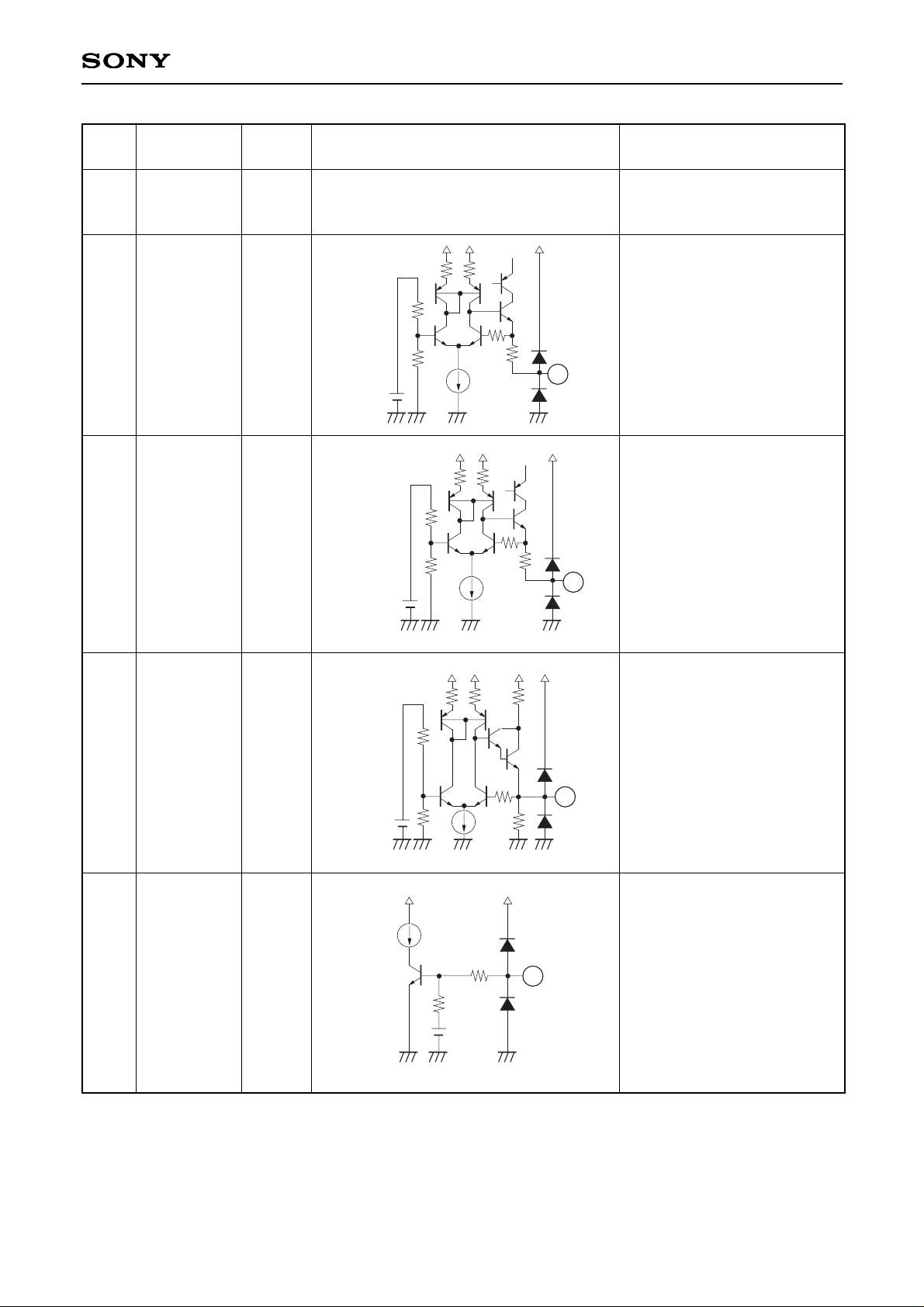
– 12 –
43 IR1
1.9
Pin to determine REC
amplifier gain.
The reference current is
produced by connecting
15kΩ between this pin and
GND.
42 GND 0
GND pin for all components
other than REC amplifier and
PB amplifier.
44 IR 1.9
Pin to produce the reference
current for the middle tune,
dropout detector and ramp.
Connect 18kΩ between this
pin and GND.
45 VG2 2.45
2.45V internal reference
voltage source.
46 PCMIN 2.45
Recording PCM input pin.
Input after cutting DC
component with C.
Input level: 300mVp-p (typ.)
43
1k
20k
40µ
40k
40k
4.15V
1k
20k
40µ
42k
40k
4.15V
44
20k
75µ
34.5k
49k
4.15V
45
270
4k
143
70µ
50k
2.45V
46
Pin
No.
Symbol
Pin
voltage
Equivalent circuit Description
Page 13
CXA2002R
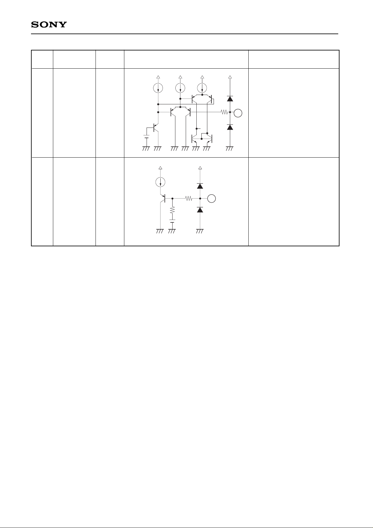
– 13 –
Pin
No.
47 PCMREC —
PCM recording switchover pin.
PCM recording is performed
when this pin goes high.
High: 2.3V or above
Low: 0.6V or below
48 ATFIN 2.45
Recording ATF input pin.
Input after cutting DC
component with C.
Input level: 125mVp-p (typ.)
Symbol
Pin
voltage
Equivalent circuit Description
143
35µ35µ35µ
1.5V
47
143
70µ
50k
2.45V
48
Page 14
CXA2002R
– 14 –
IC internal consumption current
(including REC amplifier output bias
current) during switched recording.
IC internal current during playback.
IC internal current (including REC
amplifier output bias current) during
after-recording.
Measure the pin voltage.
Measure the pin voltage.
Pin 7 (YLEVEL) = 3.15V
Adjust Pin 7 (YLEVEL) so that Pin
41 (RECVIDEO) output level
becomes 200mVp-p
→ VYLEV
Pin 7 (YLEVEL) = 0.0V
14MHz level/300kHz level
Pin 7 (YLEVEL) = V
YLEV
Pin 7 (YLEVEL) = VYLEV
Pin 5 (LOWLEVEL) = 3.15V
Pin 7 (YLEVEL) = VYLEV
Adjust Pin 5 (LOWLEVEL) so that
Pin 41 (RECVIDEO) output level
becomes 12.5mVp-p → V
ILEV
Pin 7 (YLEVEL) = VYLEV
Pin 5 (LOWLEVEL) = 0.0V
Pin 7 (YLEVEL) = V
YLEV
Pin 5 (LOWLEVEL) = 0.0V
Pin 7 (YLEVEL) = V
YLEV
1
2
3
4
5
6
7
8
9
10
11
12
13
14
IREC
IPB
IAFREC
VREG
VG2
GYmin
G
YcenGYmax
V
FY
DY
GlVmin
Gl
Vcen
Gl
Vmax
D
AFM
—
—
—
—
—
6
6
6
6
6
2
2
2
2
—
—
—
—
—
500mVpp
500mVpp
200mVpp
500mVpp
500mVpp
125mVpp
125mVpp
125mVpp
125mVpp
—
—
—
—
—
300kHz
300kHz
300kHz
14MHz,
300kHz
7MHz
1.7MHz
1.7MHz
1.7MHz
1.7MHz
A
G
I
A
A
A
A
A
A
A
A
A
A
A
IVCC1+
IVCC2
IVCC1+
IVCC2
IVCC1+
IVCC2
39
45
41
41
41
41
41
41
41
41
41
33
26
45
3.95
2.30
—
—
–3.6
–1.5
—
—
—
–14.0
—
47
37
64
4.15
2.45
–23.2
–8.0
–1.3
–0.5
–55
–30.4
–20
–11.6
–55
61
48
83
4.35
2.60
–14.1
—
—
+0.5
—
–26.0
—
—
—
mA
mA
mA
V
V
dB
dB
dB
dB
dB
dB
dB
dB
dB
Current consumption for
recording
Current consumption for
playback
Current consumption for after-
recording
VREG pin voltage
VG2 pin voltage
Recording system
Y signal GCA min. gain
Y signal GCA center gain
Y signal GCA max. gain
Y signal GCA frequency
response (center gain)
Y signal GCA secondary distortion (center gain)
Low-band signal GCA (VIDEO
path) min. gain
Low-band signal GCA (VIDEO
path) center gain
Low-band signal GCA (VIDEO
path) max. gain
AFM path secondary distortion
Electrical Characteristics
∗
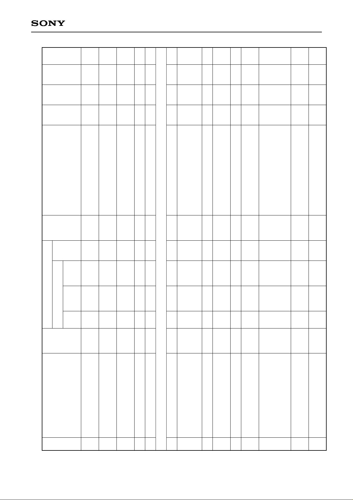
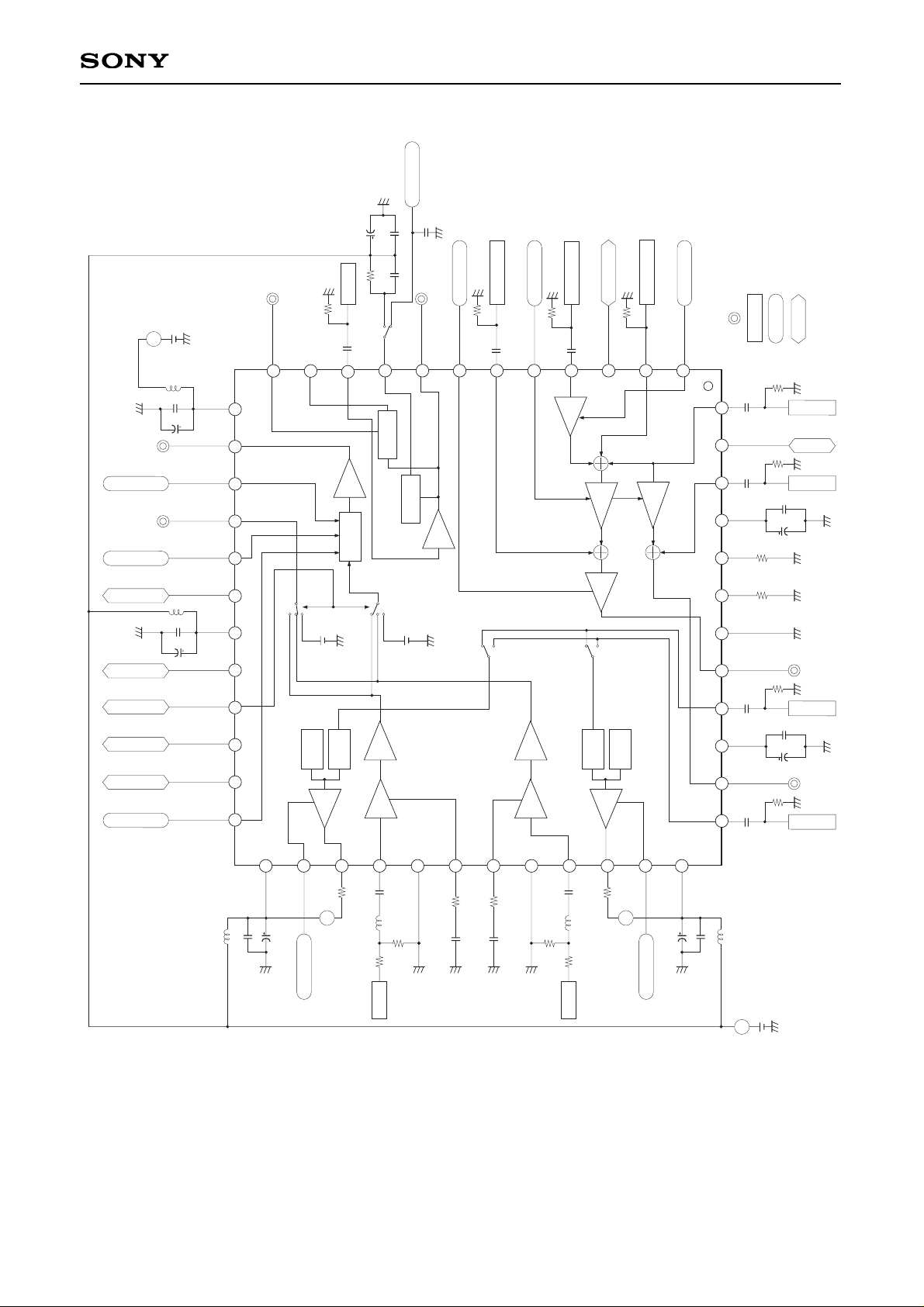
See the Control Logic Truth Table for control logic conditions. (Vcc = 4.75V, VccEVR = 3.15V, Ta = 25°C. See the Electrical Characteristics Measurement Circuit.)
No. Item Symbol
Measurement conditions
Input condition
Input
pin
Level
Fre-
quency
Control
logic
Measure-
ment
point,
ammeter
name
Measurement method Min. Typ. Max. Unit
Page 15
CXA2002R
– 15 –
Pin 5 (LOWLEVEL) = 0.0V
Pin 7 (YLEVEL) = V
YLEV
Pin 5 (LOWLEVEL) = 3.15V
Pin 5 (LOWLEVEL) = 0.0V
Pin 5 (LOWLEVEL) = VlLEV
Pin 7 (YLEVEL) = VYLEV
Pin 1 (CCONT) = 3.15V
Adjust Pin 1 (CCONT) so that Pin
41 (RECVIDEO) output level
becomes 50mVp-p→V
CLEV
Pin 5 (LOWLEVEL) = VlLEV
Pin 7 (YLEVEL) = VYLEV
Pin 5 (LOWLEVEL) = VlLEV
Pin 7 (YLEVEL) = VYLEV
Pin 1 (CCONT) = 0.0V
Pin 5 (LOWLEVEL) = VlLEV
Pin 7 (YLEVEL) = VYLEV
Pin 1 (CCONT) = VCLEV
2MHz level/300kHz level
Pin 5 (LOWLEVEL) = VlLEV
Pin 7 (YLEVEL) = VYLEV
Pin 1 (CCONT) = VCLEV
14MHz gain/300kHz gain
Measure DC currents.
Pin 26 (REC1CONT),
Pin 35 (REC2CONT) = 3.3V
15
16
17
18
19
20
21
22
23
24
25
26
G
VATF
GPATF1
GPATF2
Gcmin
Gccen
Gcmax
V
FC
DC
GP
VFP
DP
IB1
IB2
48
48
48
4
4
4
4
4
46
46
46
—
125mVpp
125mVpp
125mVpp
300mVpp
300mVpp
300mVpp
300mVpp
300mVpp
300mVpp
300mVpp
300mVpp
—
100kHz
100kHz
100kHz
300kHz
300kHz
300kHz
2MHz
300kHz
750kHz
300kHz
14MHz
300kHz
7MHz
—
A
A
A
A
A
A
A
A
A
A
A
B
A
41
38
38
41
41
41
41
41
38
38
38
IB1
IB2
–14.0—–14.0
—
—
–13.3
–0.5
—
–4.5
–0.8
—
14.55
–11.6
–30.7
–11.9
–26.4
–15.6
–10.5
0
–50
–3.7
0.0
–55
18.8
—
–26.0
—
–21.6
—
—
+0.5
—
–2.9
+0.8
—
23.05
dB
dB
dB
dB
dB
dB
dB
dB
dB
dB
dB
mA
ATF (VIDEO path) max. gain
ATF (PCM path) min. gain
ATF (PCM path) max. gain
Chroma signal GCA min. gain
Chroma signal GCA center gain
Chroma signal GCA max. gain
Chroma signal GCA frequency
response (center gain)
Chroma signal GCA secondary
distortion (center gain)
PCM signal path gain
PCM signal path frequency
response
PCM signal path secondary distortion
REC amplifier output
bias current
1ch
2ch
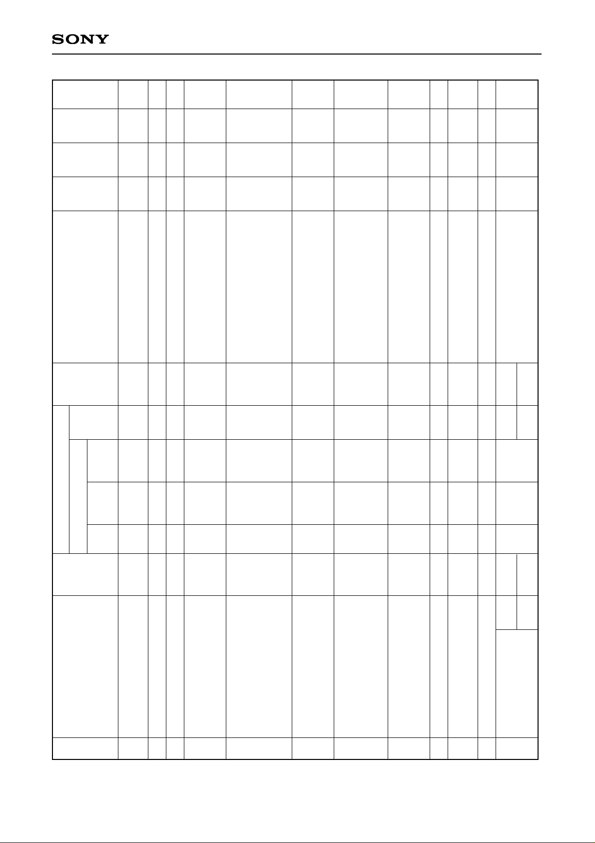
No. Item Symbol
Measurement conditions
Input condition
Level
Measurement method Min. Typ. Max. Unit
Input
pin
Fre-
quency
Control
logic
Measure-
ment
point,
ammeter
name
Page 16

CXA2002R
– 16 –
Pin 26 (REC1CONT),
Pin 35 (REC2CONT) = 3.3V
Output level (Vp-p)/51 (Ω)
27
I
R1
IR2
1ch
2ch
1ch
2ch
40 200mVpp 1MHz
B
A
27
34
18.1 20.7 23.3 mApp
REC amplifier output
current
10MHz level/1MHz level
28
V
FR1
VFR2
40
200mVpp
10MHz
1MHz
B
A
B
A
B
A
K
H
H
G
G
H
G
G
G
27
34
27
34
27
34
27
34
14
16
8
8
8
— –0.2 — dB
— 32 — µA/µs
— 32 — µA/µs
— 17 — µA/µs
58.0 61.5 65.0 dB
57.7 61.2 64.7 dB
340
315
—
Pin 15 (MTG) = 3.15V
Measure the output level, applying
a time constant to Pin 9
(RFAGCTC).
410
380
420
480
—
490
mVpp
mVpp
mVpp
REC amplifier frequency
response
1ch
2ch
29
Ton1
21
See the
Measurement
method.
22
See the
Measurement
method.
Ramp rising slope 1
1ch
2ch
30
Toff
Ramp falling slope
1ch
2ch
1ch
2ch
1ch
2ch
G
V1
GV2
GP1
GP2
VAGC1
VAGC2
VAGC3
28
33
28
33
10
10
10
200µVpp
200µVpp
224mVpp
56mVpp
896mVpp
300kHz
300kHz
7MHz
7MHz
7MHz
31
32
33
34
35
36
Head amplifier MTOUT
gain
Head amplifier
PCMOUT gain
RFAGC standard output
RFAGC cover-range high
RFAGC cover-range low
Ton2
Ramp rising slope 2
2500µsec
Input
Output
H
L
∗
Logic is inverted in
CH2 measurement.
Slope: ToffSlope: Ton1
2500µsec
Input
Output
H
L
Slope: Ton2
Playback system
No. Item Symbol
Measurement conditions
Input condition
Level
Measurement method Min. Typ. Max. Unit
Input
pin
Fre-
quency
Control
logic
Measure-
ment
point,
ammeter
name
Page 17
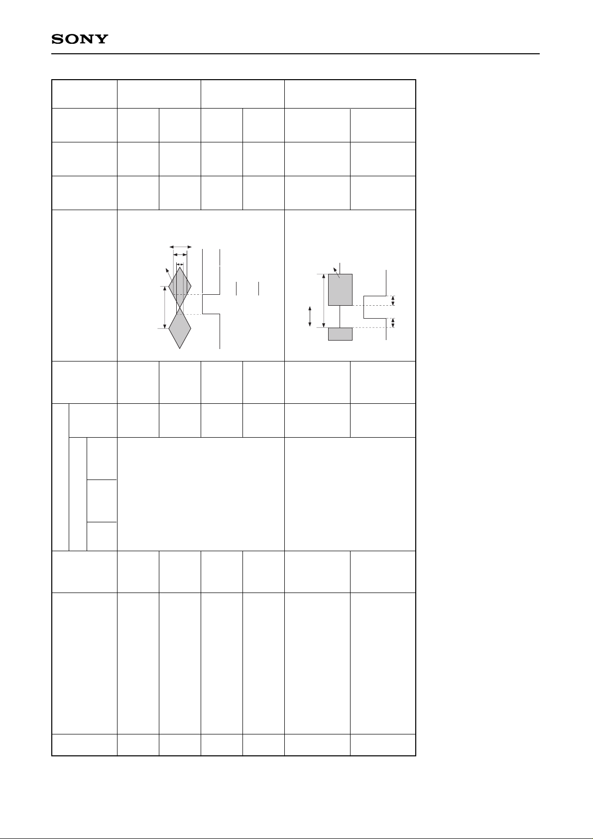
CXA2002R
– 17 –
No. Item Symbol
Measurement conditions
Input condition
Level
Measurement method Min. Typ. Max. Unit
37
Kdop-on
See the Measurement
method (figure to the
right).
See the Measurement
method (figure to the
right).
G 12 –15.0 –12.0 –9.0
dB
V
Dropout detection ON level
38 Kdop-off
G 12 –9.5 –6.5 –3.5
Dropout detection OFF level
39
Vdop-l
G 12 0 0.01 0.2
Dropout pulse low level
40 Vdop-h
G 12 2.9 3.15 3.4
µs
— 1.1 —
— 2 —
Dropout pulse high level
41 Tdop-on G 12
G 12
Dropout ON detection time
42 Tdop-offDropout OFF detection time
10kHz
7MHz
a
b
224mVp-p
V
DOP-h
VDOP-l
Pin 12
(DOP)
Pin 10 (RFAGCIN)
Apply a time constant to Pin 9 (RFAGCTC).
Kdop-on = 20 log
Kdop-off = 20 log
224
a
224
b
50µs
5kHz
Tdop-on Tdop-off
Pin 12 (DOP)
7M/224mVp-p
Pin 10 (RFAGCIN)
Input
pin
Fre-
quency
Control
logic
Measure-
ment
point,
ammeter
name
Page 18
CXA2002R
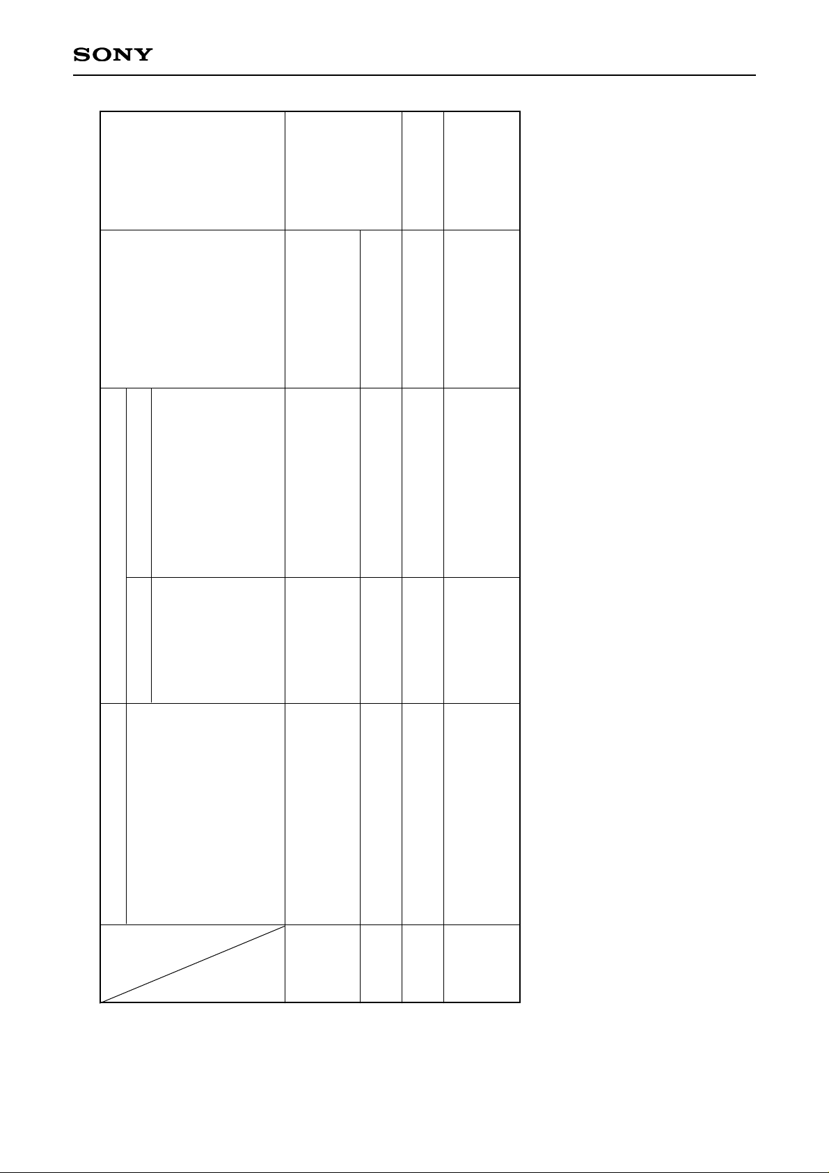
– 18 –
Input
condition
and
operation
Control
logic
conditions
A
B
C
D
E
F
G
H
I
J
K
H
L L L L L L L
L L H L L L L
L H L L L L L
L H H L L L L
L H L L L H L
L H H L L H L
H L L L — L L
H L H L — L L
H L L H L H H
H L H H L H H
H L L H H H H
H L H H H H H
x x x x x x
x x x x x x
x x x x x x
x x x x x x
x x x x x x
x x x x x x
O O CH1 CH2 O O
O O CH2 CH1 O O
x O Mute Mute Hold O
O x Mute Mute Hold O
x O Mute Mute Hold O
O x Mute Mute Hold O
VIDEO EACH REC
↓
VIDEO BOTH REC
↓
PCM REC
↓
PB
↓
After-recording
↓↓↓
REC
PB
PCM after-recording
V ∗ ∆ V
V ∗ V ∆
V ∗ V V
V ∗ V V
V P P V
V P V P
x x x x
x x x x
x P P x
x P x P
x P P x
x P x P
Control logic input condition
18 RP PB
20 BOTH REC
21 RFSWP
22 RAMP
23 RAMPCONT
47 PCMREC
3 AFREC
41 RECVIDEO
38 RECPCM
27 REC1OUT
34 REC2OUT
PB1chAmp
PB2chAmp
16 PCMOUT
14 MTOUT
8 RFAGCOUT
Dropout detector
Operation of each section under respective input condition
Recording Playback
Operation Mode
Control Logic Truth Table
After-recording mode RAMPCONT = L : Recording bias current rising slope 32µA/µs (typ.)
RAMPCONT = H : Recording bias current falling slope 17µA/µs (typ.)
(Description of input conditions) (Description of operation mode)
H : Control logic input voltage 2.3V or above O : Operating ∗ : Operating with no signal output
L : Control logic input voltage 0.6V or below x : Not operating ∆ : Operating with bias current turned off
— : Indenpendent of H and L V : Video signal is selected. Mute : Signal is muted.
P : PCM signal is selected. Hold : Time constant is kept on hold.
CH1 : CH1 signal is output.
CH2 : CH2 signal is output.
Page 19
HEAD
REC
V/I
RAMP
GEN
15dB
40dB
VPSW1
VPSW2
PCM
VIDEO
YGCA
1
1
1
1
1
1
2
CGCA
LOWGCA
LOWGCA
RF
AGC
AGCDET
DOCDET
M · T
–6dB
12dB
MUTE
2CH
1CH
MUTE
2CH
1CH
PCMSW
VIDEOSW
REC
HEAD
40dB
15dB
V/I
RAMP
GEN
RAMPCONT
RAMP
RFSWP
BOTH REC
RP PB
MTQ
MTF0
MTG
10µ
0.1µ
10µ
10µ
0.1µ
10µ
A
PCMOUT
MTOUT
RAMPCONT
RAMP
RFSWP
BOTH REC
RP PB
MTQ
MTF0
MTG
PCMOUT
MTOUT
REC1CONT
10µ
0.1µ
100µ
A
PB1IN
5.6µ
0.01µ
0.022µ
390
0.022µ
390
PB2IN
5.6µ
0.01µ
49
49
REC2CONT
10µ
0.1µ
100µ
A
A
IVCC1
V
CC
4.75V
IVCC2
V
CC EVR
3.15V
DOP
YLEVEL
RFAGCIN
RFAGCOUT
LOWLEVEL
YIN
CIN
AFREC
AFMIN
CCONT
VPPCMIN
RECPCM
RECVIDEO
VPVTRIN
PCMIN
ATFIN
PCMREC
40
39
38
37
41
42
43
44
45
46
47
48
2
3
4
5
6
7
8
9
10
11
12
1
13
1415
16
17
18
19
20
21
22
23
24
25
26
27
28
29
30
36
35
34
31
32
33
VPPCMIN
RECPCM
VPVTRIN
RECVIDEO
VREG
GND
IR1
IR
VG2
PCMIN
PCMREC
ATFIN
0.01µ
51
0.1µ
10µ
0.01µ
51
15k
∗
18k
∗
0.1µ
10µ
51
51
0.01µ
51
0.01µ
0.01µ
51
0.01µ
51
CCONT
AFMIN
AFREC
CIN
LOWLEVEL
YIN
YLEVEL
RFAGCOUT
RFAGCTC
RFAGCIN
DOCDET
DOP
470k
4700p
10µ
0.1µ
0.01µ
51
1
1
VCC2
REC2CONT
51
∗
REC2OUT
PB2IN
PBDUMP2
PBDUMP1
GND1
PB1IN
REC1OUT
REC1CONT
V
CC1
GND2
Signal output pin
Signal input pin
EVR adjusting pin
Control logic pin
Resistance accuracy 1%
∗
V
CC
V
CC
EVR
0.01µ
RFAGCTC
IB1
IB2
PCM
VIDEO
51
∗
CXA2002R
– 19 –
Electrical Characteristics Measurement Circuit
Page 20
CXA2002R
– 20 –
HEAD
REC
V/I
RAMP
GEN
15dB
40dB
VPSW1
VPSW2
PCM
VIDEO
YGCA
1
1
1
1
1
1
2
CGCA
LOWGCA
LOWGCA
RF
AGC
AGCDET
DOCDET
M · T
–6dB
12dB
MUTE
2CH
1CH
MUTE
2CH
1CH
PCMSW
VIDEOSW
REC
HEAD
40dB
15dB
V/I
RAMP
GEN
RAMPCONT
RAMP
RFSWP
BOTH REC
RP PB
MTQ
MTF0
MTG
PCMOUT
MTOUT
VPPCMIN
RECPCM
VPVTRIN
RECVIDEO
VREG
GND
IR1
IR
VG2
PCMIN
PCMREC
ATFIN
CCONT
AFMIN
AFREC
CIN
LOWLEVEL
YIN
YLEVEL
RFAGCOUT
RFAGCTC
RFAGCIN
DOCDET
DOP
V
CC2
REC2CONT
REC2OUT
PB2IN
PBDUMP2
PBDUMP1
GND1
PB1IN
REC1OUT
REC1CONT
V
CC1
GND2
V
CC
V
CC EVR
2
3
4
5
6
7
8
9
10
11
12
1
13
14
15
16
17
18
19
20
21
22
23
24
25
26
27
28
29
30
36
35
34
31
32
33
40
39
38
37
41 42
43
44
46
47
48
REC2CONT
REC1CONT
RAMPCONT
RAMP
RFSWP
BOTH REC
RP PB
EVR LOGIC
AFM TRAP ATF TRAP C TRAP RF EQ
PB C RF
PB RF
PCM OUT
RFAGCOUT
RFVCC1
RFVCC2
DOP
MTQ
MTF0
MTG
YLEVEL
LOWLEVEL
CCONT
YIN
CIN
AFMIN
ATFIN
PCMIN
SIGNAL OUT
EVR
SIGNAL IN
LOGIC
AFREC
PCMREC
RFGND
CH1 HEAD
100µ
0.1µ
10µ
0.01µ
0.022µ390
0.022µ390
0.01µ
CH2 HEAD
100µ
0.1µ
10µ
0.1µ
10µ
0.01µ 0.01µ
15k
18k
0.1µ
10µ
0.01µ
0.01µ
45
0.01µ
0.01µ
4700p
470k
100µ
10µ
0.1µ
PCM
VIDEO
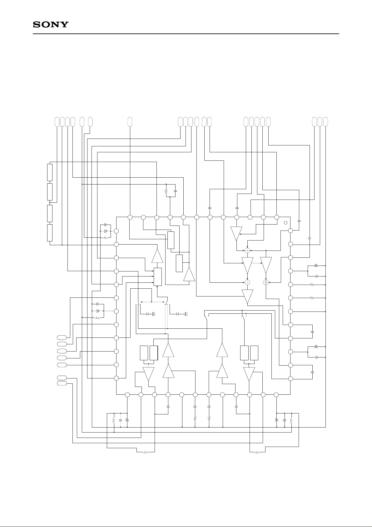
Application Circuit
Application circuits shown are typical examples illustrating the operation of the devices. Sony cannot assume responsibility for
any problems arising out of the use of these circuits or for any infringement of third party patent and other right due to same.
Page 21
CXA2002R
– 21 –
Description of Operation
<Mix amplifier + recording level adjustment>
Y, chroma, AFM, ATF and PCM signals are input at specified levels so that they are mixed internally to achive
an appropriate current value at the head. The VIDEO path signal (Y + chroma + AFM + ATF) is output to Pin
41 (RECVIDEO) and the PCM path signal (PCM + ATF) to Pin 38 (RECPCM). The Y level is EVR-adjusted at
Pin 8 (YLEVEL) and the low band (chroma, AFM, ATF) level at Pin 5 (LOWLEVEL). The low-band levels of the
video path and the PCM path are interlocked in adjustment.
<SW + recording amplifier>
The VIDEO path signal and the PCM path signal, which underwent recording level adjustment, are switched at
a correct timing, then converted to a current to drive the head.
A feedback dumping circuit is incorporated to inhibit head resonance, and the peaking can be adjusted by EVR
at Pin 26 (REC1CONT), Pin 35 (REC2CONT).
During recording, the output capacitance is about 12pF including that of the head amplifier.
<Head amplifier>
The playback signal from the head is amplified with low noise and high gain. A feedback dumping circuit is
incorporated to inhibit head resonance, and the peaking can be adjusted by external resistors connected to Pin
30 (PBDUMP1), Pin 31 (PBDUMP2).
During playback, the input capacitance is about 20pF including that of the recording amplifier.
<SW + middle tune>
This section switches the playback signals of CH1
and CH2 at the correct timing and outputs the
playback VIDEO signal to Pin 14 (MTOUT) and
the playback PCM signal to Pin 16 (PCMOUT). In
the PCM after-recording mode, both playback
VIDEO signal and playback PCM signal are muted
during the PCM recording period.
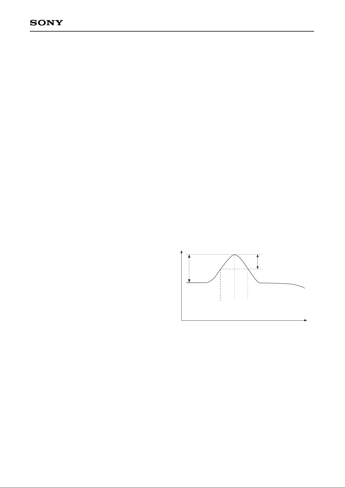
The middle tune circuit corrects the frequency
response of the playback VIDEO signal.
The center frequency can be adjusted by EVR at
Pin 17 (MTF0), Q at Pin 24 (MTQ) and the boost
at Pin 15 (MTG).
The figure to the right shows the center condition
that sets f0 = 8MHz, Q = 2.5 and the boost = 6dB.
Each control characteristics shown in "Example of
Representative Characteristics" is obtained when
two of them are fixed to the center condition.
<RFAGC>
This circuit inputs the playback Y signal separated from the playback VIDEO signal using an external circuit
and outputs it at a constant level of 410mVp-p. In the PCM after-recording mode, RFAGC gain is kept
unchanged during PCM recording period.
<Dropout detection>
A dropout is detected in the playback Y signal, and a dropout pulse is output. The detection level is optimized
using 224mVp-p input as a reference. If necessary, the detection level can be adjusted by inputting a DC
voltage to Pin 11 (DOCDET). To make this adjustment, input a voltahe proportional to the output voltage of Pin
39 (VREG).
Boost amount
= 6dB
Gain
3dB
f
1 f2
Center frequency f0 = 8MHz
Q = f
0 / (f2 – f1) = 2.5
Frequency
Page 22

CXA2002R
– 22 –
<Control logic block>
This IC exercises power-saving control of circuit blocks which are not in immediate need for operation. The IC
also incorporates a logic circuit for controlling a number of SWs which change inputs and outputs at
complicated timing.
The combinations of input and output in the basic operation are shown in the "Control Logic Truth Table".
<Reference voltage in the IC>
VG2 2.45V and VREG 4.15V are generated as a reference voltages used in the IC.
VG2 cannot be used outside the IC. VREG cannot also be used outside the IC except for adjusting the dropout
detection level at Pin 11 (DOCDET).
Notes on Operation
1. This IC is characterized by high-voltage gain (about 61dB in the playback system). Pay attention to the
following when using the IC.
1) Use reinforced power supply and ground lines. Decouple the power supply pin with a coil and a
capacitor. Connect the decoupling capacitor as close to the pin as possible.
2) Use of a regulator power supply is recommended.
3) Connecting a capacitive load to the output may cause oscillation.
4) Take particular care not to make capacitive coupling between the head amplifier input and the playback
output. Also be careful not to make capacitive coupling between the recording input and the recording
amplifier output.
5) Use of decoupling capacitors is recommended between the following DC voltage input pins and GND.
When the control voltage source is at high impedance, aggravation of cross talk or oscillation is feared to
occur.
Pin 1 (CCONT), Pin 5 (LOWLEVEL), Pin 7 (YLEVEL)
Pin 9 (RFAGCTC) [not when time constant is connected], Pin 11 (DOCDET)
Pin 17 (MTF0), Pin 24 (MTQ), Pin 26 (REC1CONT)
Pin 35 (REC2CONT)
6) When a decoupling capacitor is necessary for other pins (not power supply pin), it is recommended to
connect each decoupling capacitor as close as to the pin as possible.
2. When Pin 13 (EVR Vcc) is used for 5V system (4.75 ), the voltage of Pin 19 (Vcc) should be equal to
or larger than that of Pin 13 (EVR Vcc).
3. The voltage input to the EVR adjusting pin should be proportional to the EVR Vcc voltage. Control the input
voltage in the range from 0V to 3.15V when EVR Vcc = 3.15V.
For EVR adjustment at Pin 26 (REC1CONT) and Pin 35 (REC2CONT), control the input voltage in the range
from 1.8V to 4.75V when Vcc = 4.75V, in proportion to the supply voltage Vcc; at Pin 9 (RFAGCTC), control
the input voltage in the range from 2.5V to 4.75V.
+0.5V
–0.25V
Page 23
CXA2002R
– 23 –
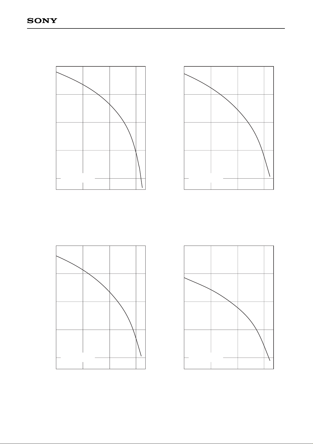
Example of Representative Characteristics
YGCA gain control
Pin 7 (YLEVEL) voltage [V]
1.0 2.0 3.0
Pin 6 (YIN) → Pin 41 (RECVIDEO) gain [dB]
–20
0
–5
–10
–15
VCC = 4.75V
EVR VCC = 3.15V
LOWGCA (VIDEO path) gain control
Pin 5 (LOWLEVEL) voltage [V]
1.0 2.0 3.0
–30
–10
–15
–20
–25
Pin 48 (ATFIN) → Pin 41 (RECVIDEO) gain [dB]
Pin 2 (AFMIN) → Pin 41 (RECVIDEO) gain [dB]
VCC = 4.75V
EVR VCC = 3.15V
LOWGCA (PCM path) gain control
Pin 5 (LOWLEVEL) voltage [V]
1.0 2.0 3.0
Pin 48 (ATFIN) → Pin 38 (RECPCM) gain [dB]
–30
–10
–15
–20
–25
VCC = 4.75V
EVR VCC = 3.15V
CGCA gain control
Pin 1 (CCONT) voltage [V]
1.0 2.0 3.0
Pin 4 (CIN) → Pin 41 (RECVIDEO) gain [dB]
–10
–15
–20
–25
VCC = 4.75V
EVR VCC = 3.15V
Page 24
CXA2002R
– 24 –
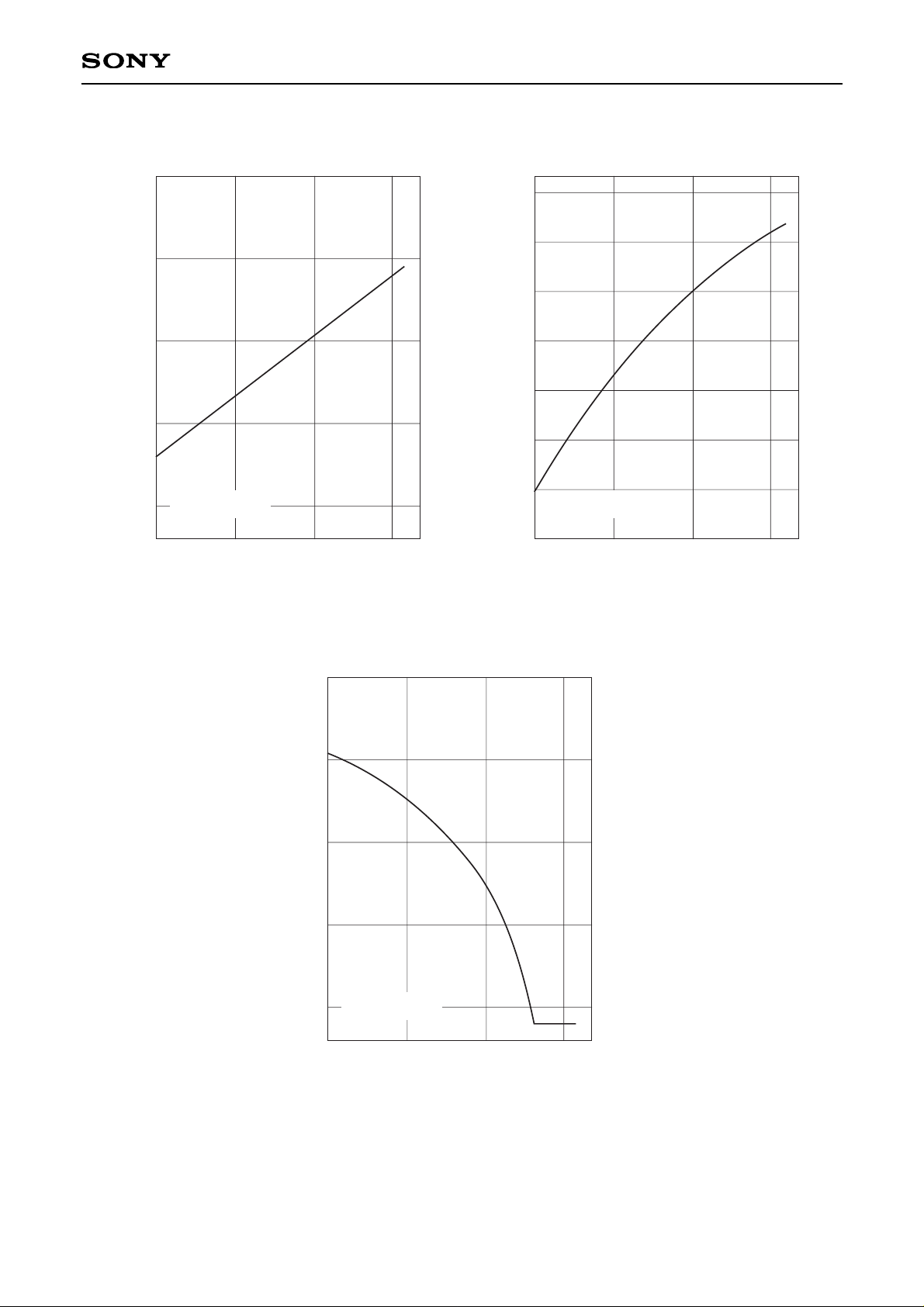
Middle tune fo control
Pin 17 (MTF0) voltage [V]
1.0 2.0 3.0
Center frequency fo [MHz]
5
15
10
VCC = 4.75V
EVR VCC = 3.15V
Middle tune Q control
Pin 24 (MTQ) voltage [V]
1.0 2.0 3.0
Q
1
6
4
VCC = 4.75V
EVR VCC = 3.15V
2
5
3
Middle tune boost control
Pin 15 (MTG) voltage [V]
1.0 2.0 3.0
Boost [dB]
5
15
10
VCC = 4.75V
EVR VCC = 3.15V
0
Page 25
CXA2002R
– 25 –
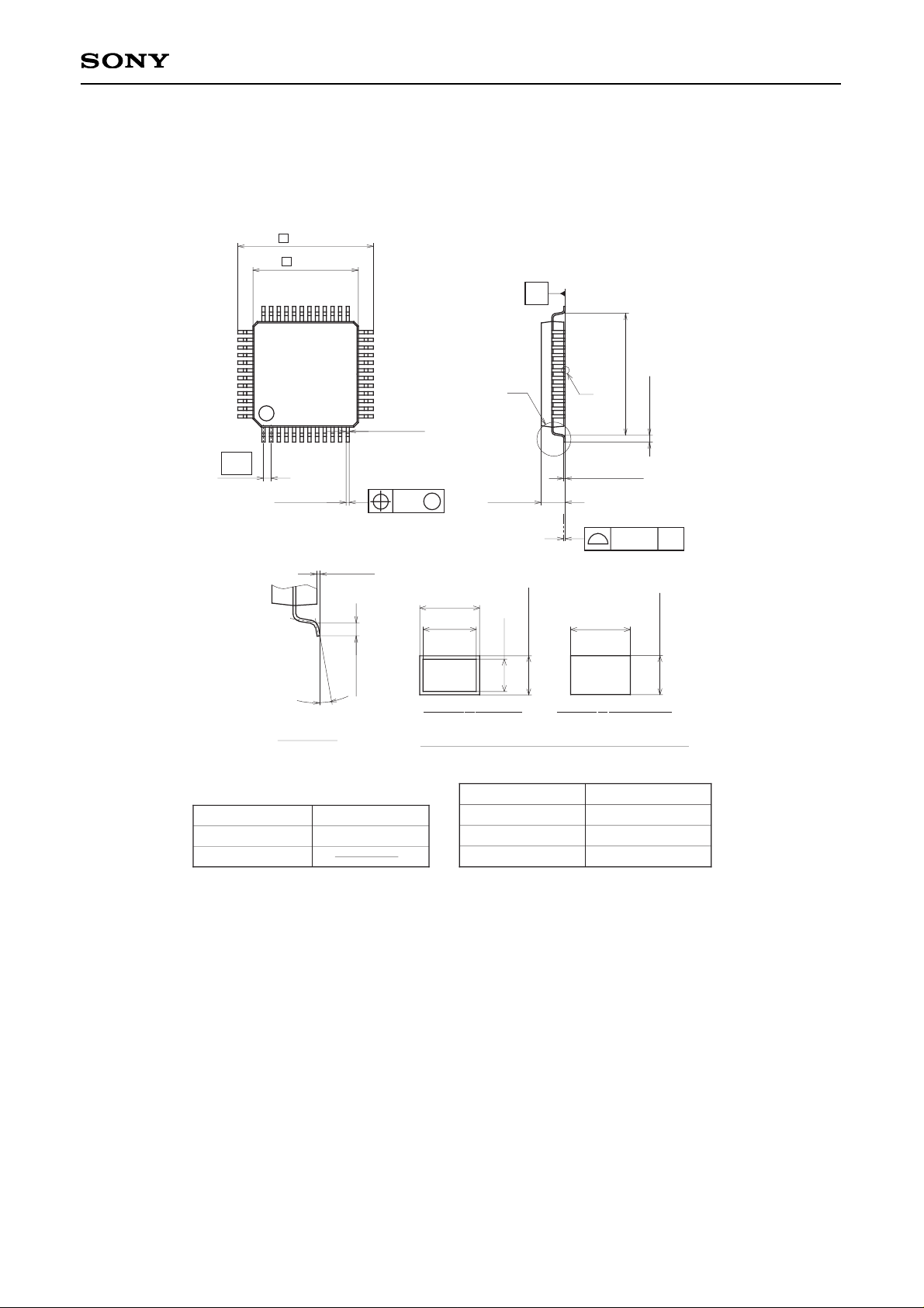
Package Outline Unit : mm
SONY CODE
EIAJ CODE
JEDEC CODE
PACKAGE MATERIAL
LEAD TREATMENT
LEAD MATERIAL
PACKAGE MASS
EPOXY RESIN
PLATING
42/COPPER ALLOY
PACKAGE STRUCTURE
48PIN LQFP (PLASTIC)
9.0 ± 0.2
∗ 7.0 ± 0.1
1
12
13
24
25
36
37
48
(0.22)
0.18 – 0.03
+ 0.08
0.2g
LQFP-48P-L01
LQFP048-P-0707
(8.0)
0.5 ± 0.2
0.127 – 0.02
+ 0.05
A
1.5 – 0.1
+ 0.2
0.1
SOLDER/PALLADIUM
NOTE: Dimension “∗” does not include mold protrusion.
0.1 ± 0.1
0.5 ± 0.2
0° to 10°
DETAIL A
0.13
M
0.5
S
S
B
DETAIL B:SOLDER
(0.18)
(0.127)
DETAIL B:PALLADIUM
0.127 ± 0.04
0.18 – 0.03
+ 0.08
0.127 – 0.02
+0.05
0.18 ± 0.03
 Loading...