

Page 1
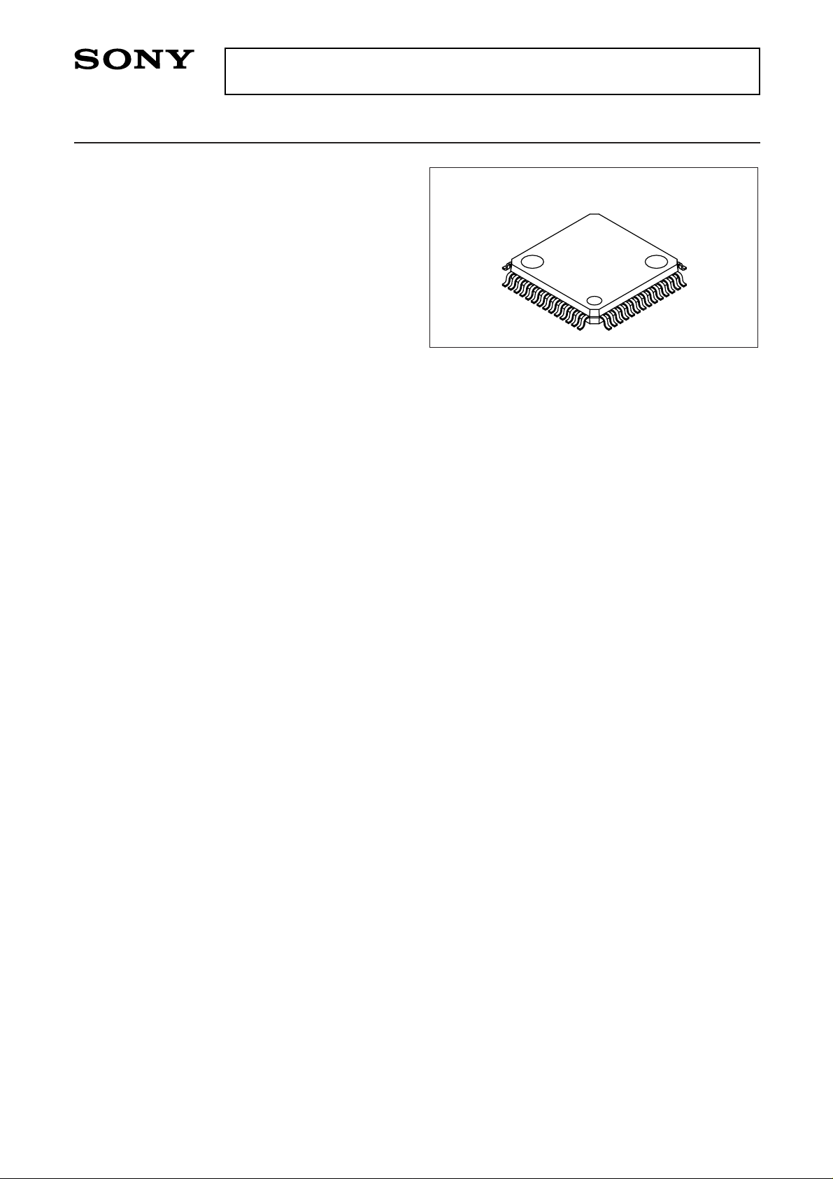
CXA2161R
I2C Bus Compatible Audio Video (AV) Switch & Electronic Volume Control
Description
The Sony CXA2161R is an Audio/Video switch
designed primarily for application in Digital Set Top
Boxes. It provides video and audio routing from the
digital encoder source to the TV and VCR scart (peritelevision) connectors. In addition, the TV audio
output has a programmable volume control. The chip
is programmed by means of an I2C interface and can
operate from a single or dual power supply.
Target specifications: Canal+, BSkyB, TPS, NorDig,
and ECCA Euro-Box
Features
Supply
• Single: 0V, +5V, +12V
• Dual: 0V, –5V, +5V and +12V
(Low number of external parts required)
Video
• 2 scart switching (VCR, TV)
• VCR input supports RGB mode
• Integrated 75Ω drivers for direct video connection
• Y/C mixer with trap for RF modulators
• Switchable clamps on inputs
• Adjustable gain on RGB outputs
• Video output shutdown for low power modes
• Fast blanking switch
• Slow blanking switch for TV and VCR output
• SVHS switch on VCR output
• Y/C auxiliary input
Audio
• Four stereo audio inputs
• Volume control (–56dB to +6dB in 2dB steps)
• Additional switchable gain on audio DAC inputs
• Audio overlay facility
• Volume bypass for TV and Phono outputs
• Mono switching on TV, VCR outputs
• High drive capability (600Ω loads possible)
• Switchable audio limiter function
• Switchable Mono output for RF modulators
• Audio output disable
I2C and Logic
• Fast mode compatible I2C bus
• Function monitor with loop through
• Interrupt output for function monitor
• Logic output pin
• Sync detector for Y/CVBS inputs
Applications
• Digital Set Top Box
• Integrated digital television
Structure
Bipolar silicon monolithic IC
Absolute Maximum Ratings (Ta = 25°C)
unless stated
• Supply voltage VCC 14 V
• Storage temperature Tstg –65 to +150 °C
• Allowable power dissipation
PD 1.1 W
(when mounted on the board)
Operating Conditions
• Single supply 12 ± 0.6 V
5 ± 0.25 V
• Dual supply –5 ± 0.25 V
5 ± 0.25 V
12 ± 0.6 V
• Operating temperature Topr –20 to +75 °C
– 1 –
E00202-PS
Sony reserves the right to change products and specifications without prior notice. This information does not convey any license by
any implication or otherwise under any patents or other right. Application circuits shown, if any, are typical examples illustrating the
operation of the devices. Sony cannot assume responsibility for any problems arising out of the use of these circuits.
56 pin LQFP (Plastic)
Page 2
– 2 –
CXA2161R
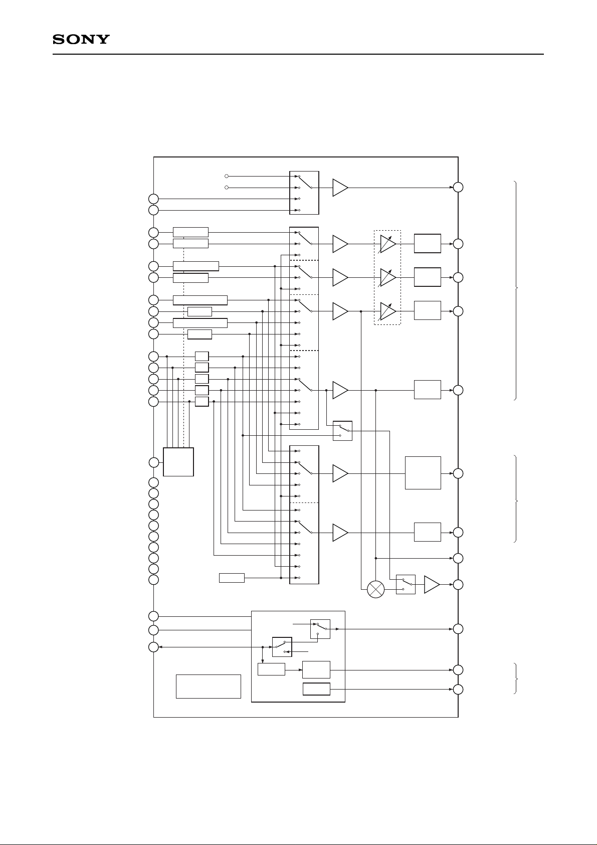
Block Diagram
(1) Video and Digital Section
Note) All video outputs contain 75Ω drivers, except VOUT_7 (Pin 38).
0/6/12V
0/6/12V
2
8
9
11
10
12
13
14
15
18
21
24
33
34
35
36
37
38
39
40
41
43
44
45
46
47
48
49
7
50
6
51
1
5
52
53
3
4
54
55
56
FBLK_SW
VIDEO SWITCH1 (TV)
RGB Gain Control
(+1, 2, 3dB)
VIDEO SWITCH2 (VCR)
DC Restore
DC Restore
DC Restore/Tip
DC Restore/C bias
C bias
DC Restore/C bias
C bias
Clamp Cntl
Tip
Tip
Tip
Tip
Tip
Bias
Mute
Sync
Detect
DC Restore
Monitor
3.3V or 5V
Fast Mode
Compatible
Logic
Interrupt
Control
×2
Output
disable
×2
Output
disable
×2
Output
disable
×2
Output
disable
×2
Output
disable &
Bi-drection
Control
×2
Output
disable
×2
MIX_SW
MIX_SW
TV_FBLK
FBLK_IN1
+3.5V
0V
FBLK_IN2
VIN_1
VIN_2
VIN_3
VIN_4
VIN_5
VIN_6
VIN_7
VIN_13
VIN_8
VIN_9
VIN_10
VIN_11
VIN_12
SYNC_ID
AUD_BIAS
VID_BIAS
+5V/12V_V
CCA
–5V_GNDA
+5V_DIG
GND_DIG
+5V_VOUT
GND_VID
+5V_VID
+12V_DIG
SDA
SCL
FNC_VCR
DIG
VCR
DIG BLUE
VCR BLUE
DIG GREEN/CVBS
VCR GREEN
DIG RED/CHROMA
DIG CHROMA
VCR RED/CHROMA
AUX CHROMA
DIG CVBS/LUMA
DIG CVBS/LUMA
VCR CVBS/LUMA
TV CVBS
AUX Y/CVBS
VCR
Typical Connection
↓
Typical Connection
↓
VOUT_1
TV BLUE
VOUT_2
TV GREEN
TV
VCR
RF MOD
TV
MICRO
VOUT_3
TV RED/C
VOUT_4
TV CVBS/Y
VOUT_5
VCR CHROMA
VOUT_6
VCR CVBS/Y
TRAP
VOUT_7
(CVBS)
FNC_TV
INTRUPT
LOGIC
Page 3
– 3 –
CXA2161R
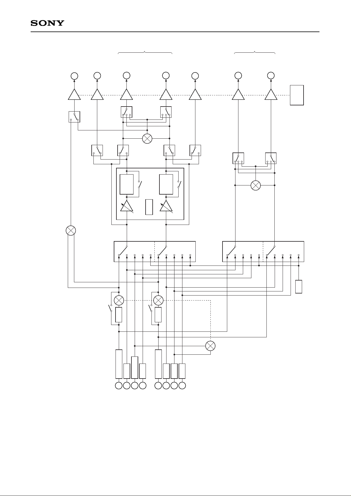
(2) Audio section
27
6dB
Vol Bypass
(TV)
AUDIO SWITCH1 (TV)
17
20
23
26
25
30
31
32
42
–6/–3/0/+3dB
–6dB
–6dB
–6/–11dB
16
19
22
29
–6/–3/0/+3dB
–6dB
–6dB
–6dB
AUDIO SWITCH2 (VCR)
RIN_1 (DIG)
MONO
To RF Modulator
PHONO_R
RTV
LTV
PHONO_L
ROUT1
LOUT1
VCR
RIN_2 (VCR)
RIN_3 (TV/OVERLAY)
RIN_4 (AUX)
LIN_1 (DIG)
LIN_2 (VCR)
LIN_3 (TV/OVERLAY)
LIN_4 (AUX)
–16dB
Overlay on/off
–16dB
Tone mix
Overlay on/off
Bias
Mute
Limiter
2.2Vrms
Output
Disable
2dB
Limiter
2.2Vrms
2dB
Volume Control
+6 to –56dB
ZCD
Vol Bypass
(Phono)
Mono Switch
Mono and
R/L Switch
Mono and R/L
Switch
Vol Bypass
(TV)
Vol Bypass
(Phono)
6dB
6dB
6dB
6dB
6dB
6dB
TV
28
Page 4
– 4 –
CXA2161R
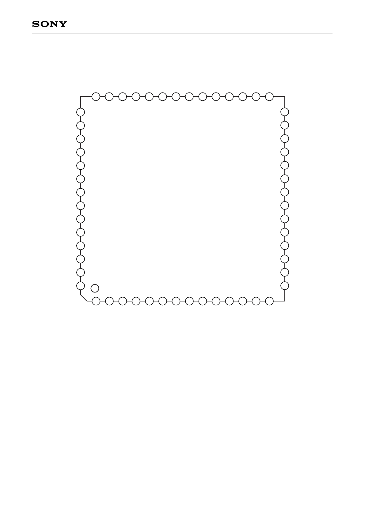
Pin Configuration
VOUT_4
+5V_VOUT
VOUT_3
VOUT_2
VOUT_1
+5V_VID
VID_BIAS
VIN_1
VIN_3
VIN_5
VIN_6
VIN_8
VIN_9
VIN_12
VIN_13
SYNC_ID
VIN_11
VIN_10
VIN_7
VlN_4
VIN_2
GND_DIG
TV_FBLK
FBLK_IN1
FNC_TV
FBLK_IN2
FNC VCR
+5V_DIG
RIN_4
VOUT_5
GND_VID
VOUT_6
VOUT_7
TRAP
INTRUPT
SCL
SDA
LOGIC
MONO
PHONO_R
PHONO_L
LlN_4
1 2 3 4 5 6 7 8 9 11 12 13 14
15
16
17
18
19
21
22
23
24
25
26
27
28
293132333435363738394142
43
44
45
46
47
48
49
50
51
52
53
54
55
56
10
20
3040
ROUT1
LOUT1
RTV
LTV
+5V/12V_V
CCA
RIN_1
LIN_1
–5V_GNDA
RIN_2
LIN_2
AUD_BIAS
RIN_3
LIN_3
+12V_DIG
Page 5
– 5 –
CXA2161R
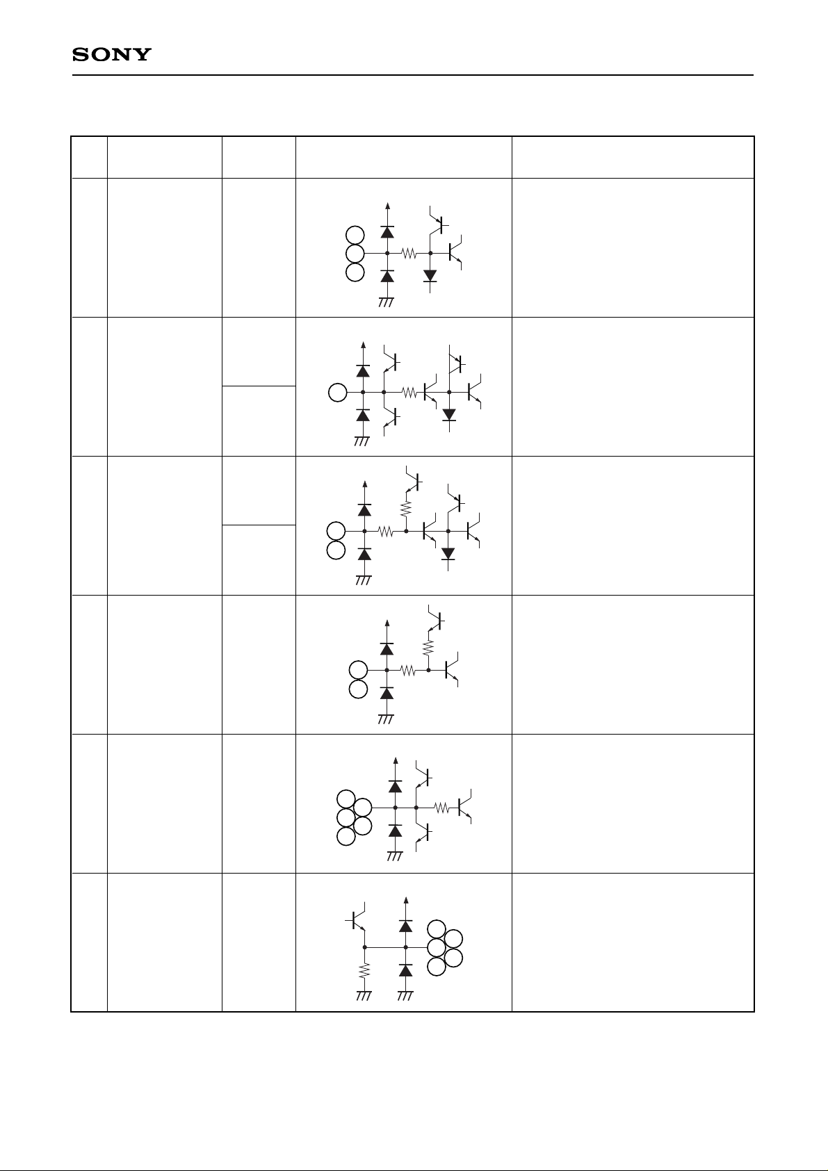
Pin Description
Pin
No.
Symbol
Pin
voltage [V]
Equivalent circuit Description
VCC
150
6
7
50
VIN_1
VIN_2
VIN_4
2.4
RGB signal inputs
50
7
6
VCC
150
51
VIN_3
2.4
2.35
RGB signal input
or
CVBS/Luminance signal input
51
VCC
150
20k
5
52
VIN_5
VIN_7
2.4
3.0
RGB signal inputs
or
Chrominance signal inputs
52
5
VCC
150
20k
1
53
VIN_6
VIN_13
3.0
Chrominance signal inputs
53
1
150
3
4
54
55
56
V
CC
VIN_8
VIN_9
VIN_10
VIN_11
VIN_12
2.35
CVBS/Luminance signal inputs
54
55
4
3
56
VCC
39
43
45
46
47
12k
VOUT_1
VOUT_2
VOUT_3
VOUT_4
VOUT_6
—
RGB/CVBS signal outputs
(See description of operation for pin
voltages)
47
46
45
43
39
Page 6
– 6 –
CXA2161R
Pin
No.
Symbol
Pin
voltage [V]
Equivalent circuit Description
VCC
12k
41
VOUT_5
1.8
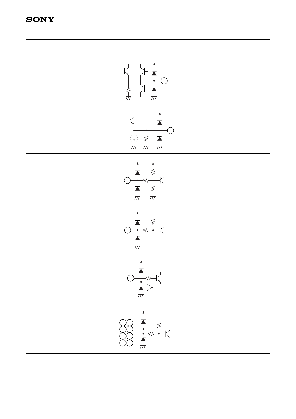
Chrominance signal output
41
VCC
12k
0.75mA
38
VOUT_7
0.4
Typically
RF modulator signal output
Minimum load resistance = 20kΩ
38
VCC VCC
150
40.8k
18.3k
49
VID_BIAS
0.9
Internal reference bias for video
circuits. A capacitor is connected
from this pin to GND.
Typically 100nF
49
VCC
200
2k
37
TRAP
2.3
Connects trap circuit for subcarrier
37
VCC
150
2
SYNC_ID
2.5
Sync detect circuit time constant,
resistor and capacitor connection pin
2
VCC
VCC/2
60k
60k
16
17
19
20
22
23
29
42
LIN_1
RIN_1
LIN_2
RIN_2
LIN_3
RIN_3
LIN_4
RIN_4
6.0
(Single)
0.0
(Dual)
Audio signal inputs
22
23
19
20
16
17
29
42
Page 7
– 7 –
CXA2161R
Pin
No.
Symbol
Pin
voltage [V]
Equivalent circuit Description
VCC
20k
25
26
27
28
30
31
32
LTV
RTV
LOUT1
ROUT1
PHONO_L
PHONO_R
MONO
6.0
(Single)
0.0
(Dual)
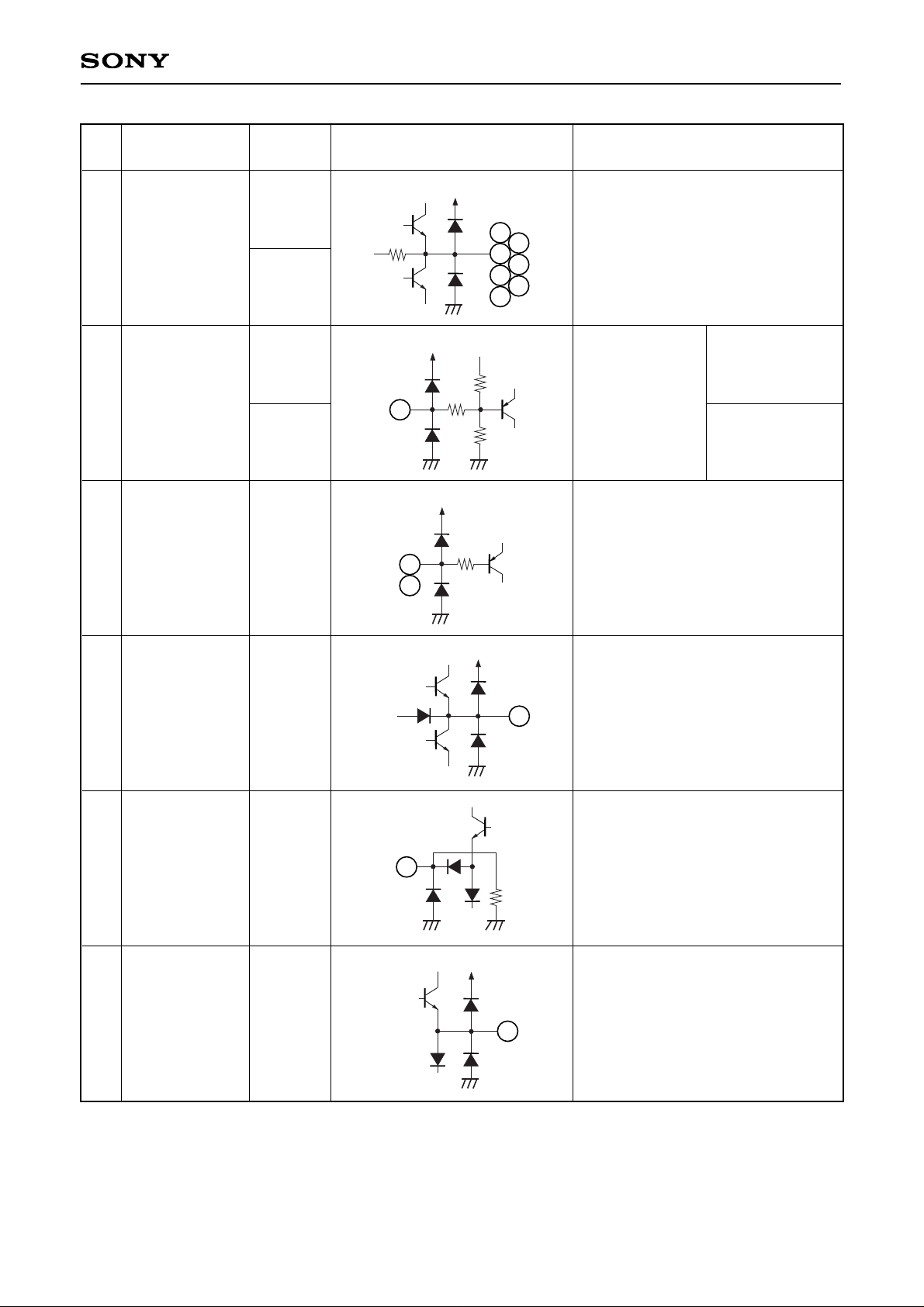
Audio signal outputs
Capacitor
connected to GND.
(Typically 22µF)
Connected
directly to GND.
25
26
27
28
30
31
32
VCC VCC
150
40k
40k
18
AUD_BIAS
Internal reference
bias for audio
circuits.
18
VCC
150
10
12
FBLK_IN1
FBLK_IN2
—
Fast blanking signal inputs
10
12
VCC
9
TV_FBLK
—
Fast blanking signal output
9
13
120k
FNC_VCR
—
SCART function pin 8 input/output to
VCR
13
VCC
11
FNC_TV
—
SCART function pin 8 output to TV
11
6.0
(Single)
0.0
(Dual)
Page 8
– 8 –
CXA2161R
Pin
No.
Symbol
Pin
voltage [V]
Equivalent circuit Description
VCC
33
36
LOGIC
INTRUPT
—
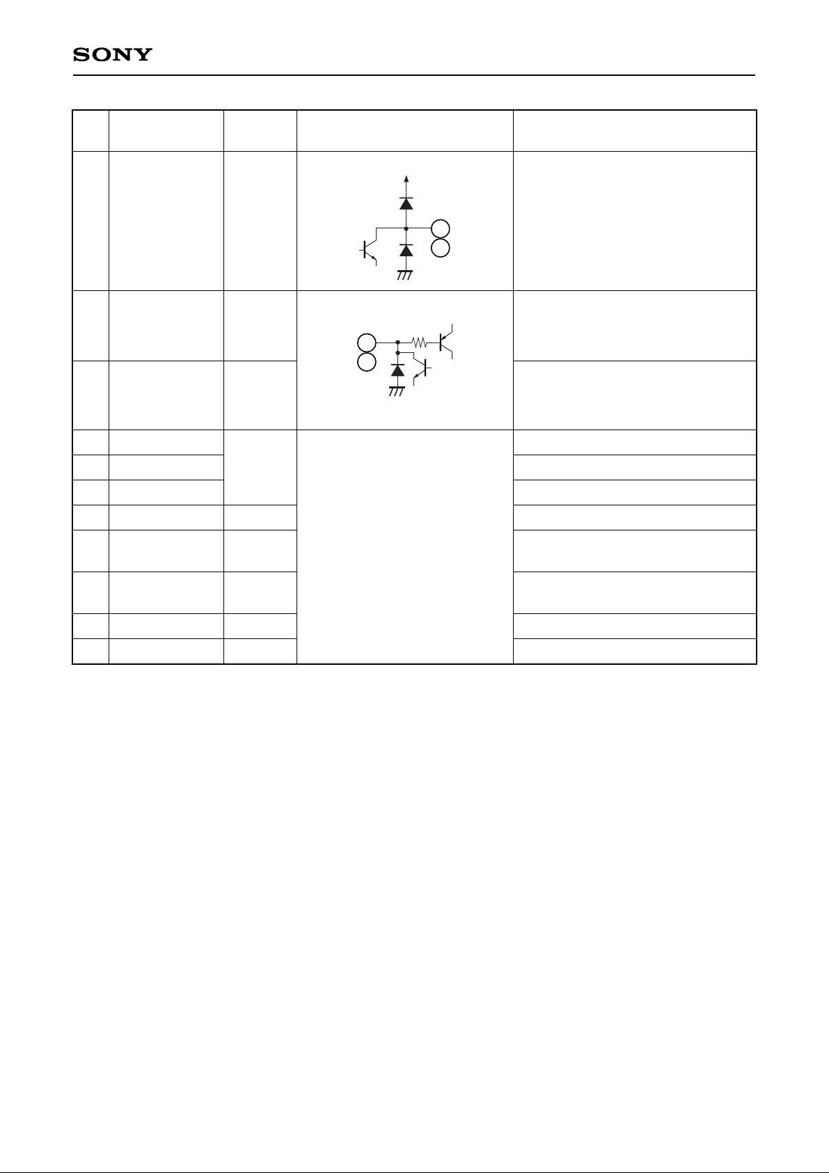
Open collector logic outputs
Typically connect to +5V through
10kΩ resistor.
33
36
8k
34
35
I2C bus clock line
I2C bus data line
+5V_DIG
+5V_VOUT
+5V_VID
+12V_DIG
–5V_GNDA
+5V/+12V_VCCA
GND_DIG
GND_VID
5.0
12.0
–5.0 (Dual)
0.0 (Single)
5.0 (Dual)
12.0 (Single)
0.0
0.0
Digital supply
Video output supply
Video supply
Digital supply
Audio supply or Audio ground
Audio supply
Digital ground
Video ground
14
44
48
15
21
24
8
40
SCL
—
—
35
SDA
34
Page 9
– 9 –
CXA2161R
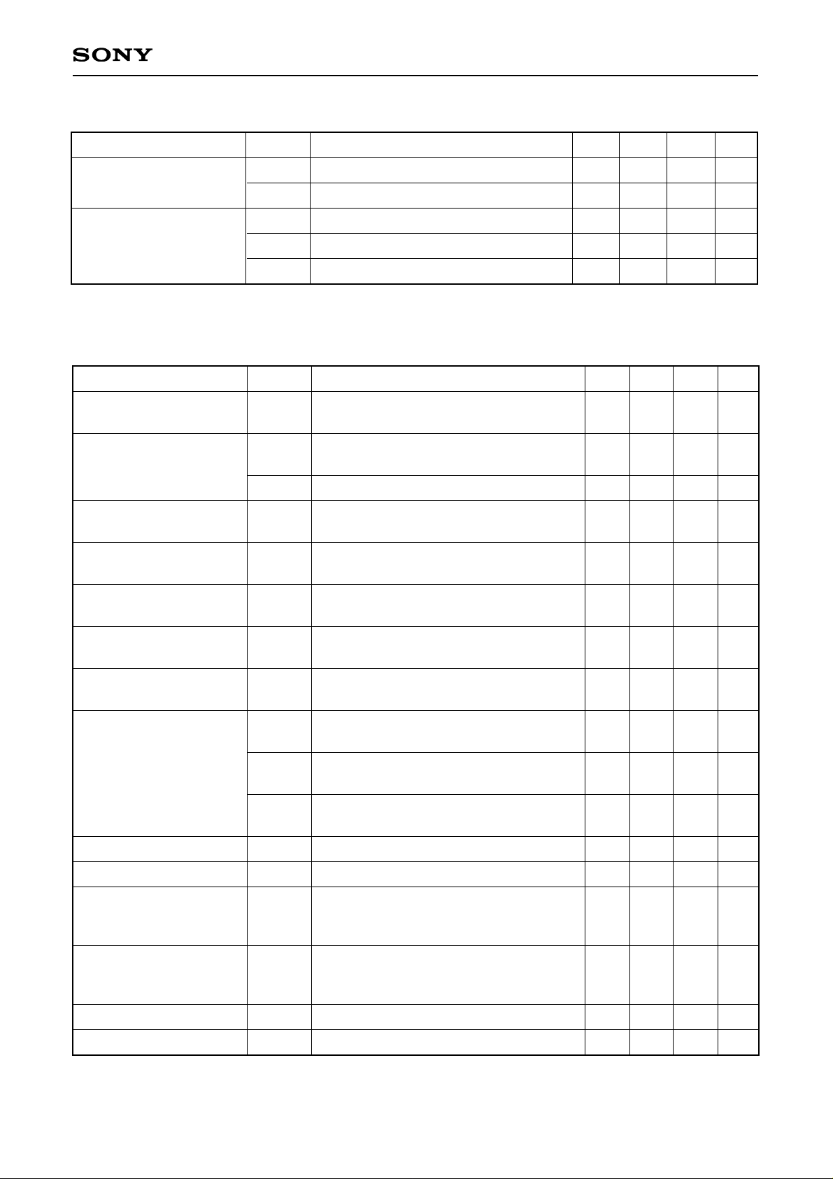
Electrical Characteristics
Nominal conditions (Ta = 25°C)
+12 supply, no signal, no load
+5 supply, no signal, no load
+12 supply, no signal, no load
+5 supply, no signal, no load
–5 supply, no signal, no load
Current consumption
(Single ended supply)
Current consumption
(Dual supply)
ICC1
ICC2
ICC3
ICC4
ICC5
—
—
—
—
—
22
50
2
70
20
45
80
6
115
45
mA
mA
mA
mA
mA
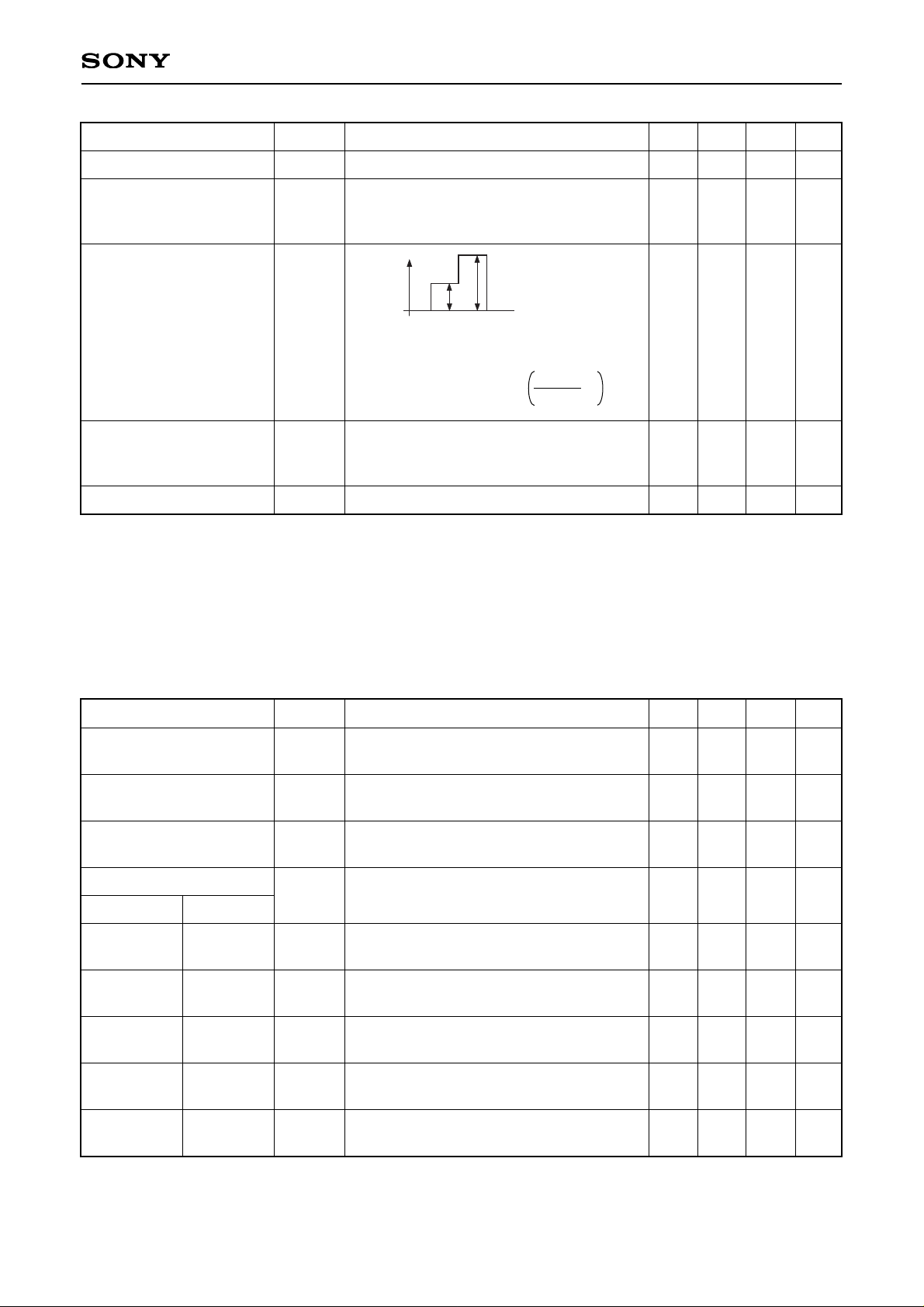
Item Symbol Conditions Min. Typ. Max. Unit
Video System
Nominal conditions single supply (Ta = 25°C, +5V/12V_VCCA = +12V, –5V_GNDA = 0V,
+5V_VID = +5V, +5V_VOUT = +5V, +5V_DIG = +5V, GND_VID = 0V)
Sync tip clamp voltage at
input
Chrominance bias input
voltage
RGB dc restore input
voltage
Sync tip clamp voltage at
output
Chrominance bias output
voltage
RGB dc restore output
voltage
Gain (Vout1 to 6)
Gain (Vout1, 2, 3)
Gain (Vout7) Mixer off
Gain (Vout7) Mixer on
Bandwidth (Vout1 to 6)
Bandwidth (Vout7)
Mixer on – No trap
components
Input dynamic range
Output dynamic range
Vclmp1
Cbias1
Cbias2
RGB1
Vclmp2
Cbias3
RGB2
GVv
GVRGB1
GVRGB2
GVRGB3
GVYC
GVYC
fV3dB
fV3dB
VDRVI
VDRVO
—
—
—
—
—
—
—
5.5
6.5
7.5
8.5
5.5
5.5
15
8
1.4
2.8
2.4
3
2.35
2.4
0.3
1.8
0.6
6.0
7.0
8.0
9.0
6.0
5.75
22
18
—
—
—
—
—
—
—
—
—
6.5
7.5
8.5
9.5
6.5
6.5
—
—
—
—
V
V
V
V
V
V
V
dB
dB
dB
dB
dB
dB
MHz
MHz
Vp-p
Vp-p
Item Symbol Conditions Min. Typ. Max. Unit
Vin3, Vin8, Vin9, Vin10, Vin11, Vin12
inputs. (Vin3 set to CVBS mode) (Fig. 1)
Vin5, Vin7 inputs. Clamps set to
Chrominance bias mode. (Fig. 1)
Vin6, Vin13 inputs. (Fig. 1)
Vin1, Vin2, Vin3, Vin4, Vin5, Vin7 inputs.
(Vin3 & Vin5 set to RGB mode) (Fig. 1)
Vout4, Vout6 outputs (Fig. 1)
Vout3, Vout5 outputs (Fig. 1)
Vout1, Vout2, Vout3 outputs (Fig. 1)
f = 200kHz, 0.3Vp-p input ,
RGB Gain = 0dB (Fig. 2)
f = 200kHz, 0.3Vp-p input ,
RGB Gain = +1dB (Fig. 2)
f = 200kHz, 0.3Vp-p input ,
RGB Gain = +2dB (Fig. 2)
f = 200kHz, 0.3Vp-p input ,
RGB Gain = +3dB (Fig. 2)
f = 200kHz, 0.3Vp-p input (Fig. 2)
f = 200kHz, 0.3Vp-p input (Fig. 2)
0.3Vp-p input, frequency where output
level is –3dB with 200kHz serving as 0dB
(Fig. 2)
0.3Vp-p input, frequency where output
level is –3dB with 200kHz serving as 0dB
(Fig. 2)
200kHz input applied to any video (Fig. 2)
200kHz input applied to any video (Fig. 2)
Page 10
– 10 –
CXA2161R
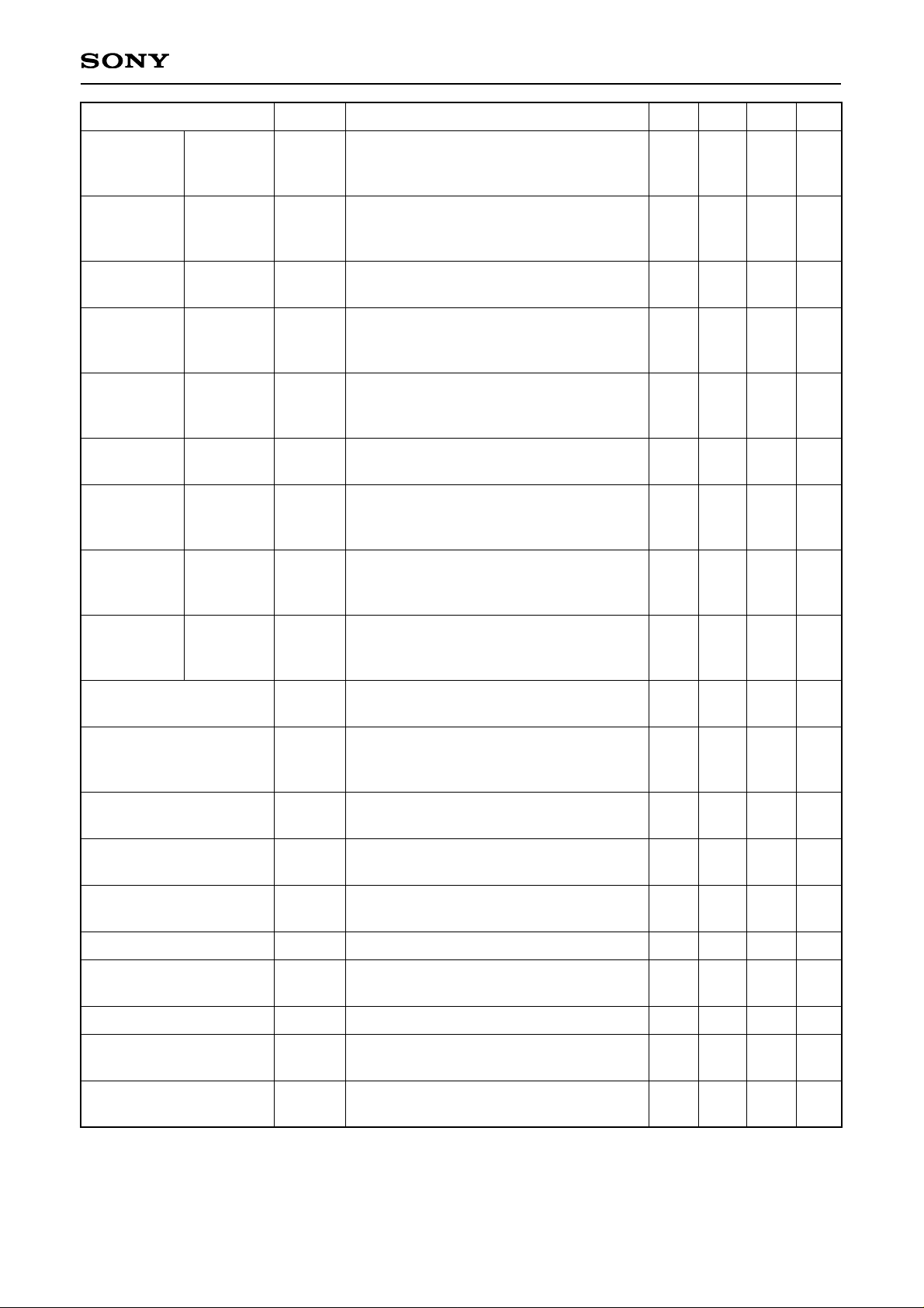
Cross talk
S/N ratio
Non-linearity
Differential gain
Differential phase
Vctv
S/NV
Lin
DG
DP
—
—
–3
–3
–3
—
74
0
0
0
–50
—
3
3
3
dB
dB
%
%
deg
Item Symbol Conditions Min. Typ. Max. Unit
f = 4.43MHz, 1Vp-p input (Fig. 2)
Ratio of 0.7Vp-p white video signal to
black line noise. Weighted using CCIR
567. HPF@5kHz, LPF@5MHz. (Fig. 2)
V1 = Pin voltage + 0.5V,
V2 = Pin voltage + 1V
At output, non-linearity = –1 × 100
(Fig. 2)
1.7Vp-p 5-step modulated staircase.
(Chrominance & Burst are 150mVp-p,
4.43MHz) (Fig. 2)
As above.
Input pin V
plus
V1
V2
V2
V1 × 2
Audio System
Unless otherwise stated: input coupling capacitor 1µF; output coupling capacitor 10µF; load 10kΩ.
Nominal conditions single supply (Ta = 25°C, +5V/12V_VCCA = +12V, –5V_GNDA = 0V, +5V_VID = +5V,
+5V_VOUT = +5V, +5V_DIG = +5V, GND_VID = 0V)
Nominal conditions dual supply (Ta = 25°C, +5V/12V_VCCA = +5V, –5V_GNDA = –5V, +5V_VID = +5V,
+5V_VOUT = +5V, +5V_DIG = +5V, GND_VID = 0V)
Input/output pin voltage
(Single supply)
Input/output pin voltage
(Dual supply)
Output pin voltage when
disabled (Dual supply)
Input
Rin1 or Lin1
Rin1 or Lin1
Rin1 or Lin1
Rin1 or Lin1
Rin1 or Lin1
VAPIN1
VAPIN2
VAPIN3
GVA1
GVA2
GVA3
GVA4
GVA5
—
—
—
–0.5
2.5
5.5
8.5
–0.5
6
0
0
0
3
6
9
0
—
—
—
0.5
3.5
6.5
9.5
0.5
V
V
V
dB
dB
dB
dB
dB
Item Symbol
Conditions
Min. Typ. Max. Unit
No signal, no load (Fig. 3)
No signal, no load (Fig. 3)
No signal, no load (Fig. 3)
f = 1kHz, 0.5Vrms input. TV volume set to
0dB, RIN_1/LIN_1 amplifier = –6dB (Fig. 4)
f = 1kHz, 0.5Vrms input. TV volume set to
0dB, RIN_1/LIN_1 amplifier = –3dB (Fig. 4)
f = 1kHz, 0.5Vrms input. TV volume set to
0dB, RIN_1/LIN_1 amplifier = 0dB (Fig. 4)
f = 1kHz, 0.5Vrms input. TV volume set to
0dB, RIN_1/LIN_1 amplifier = +3dB (Fig. 4)
f = 1kHz, 1Vrms input. TV volume set to
0dB, RIN_1/LIN_1 amplifier = –6dB (Fig .4)
Output
TV or
Phono
TV or
Phono
TV or
Phono
TV or
Phono
VCR
Gain
Page 11
– 11 –
CXA2161R
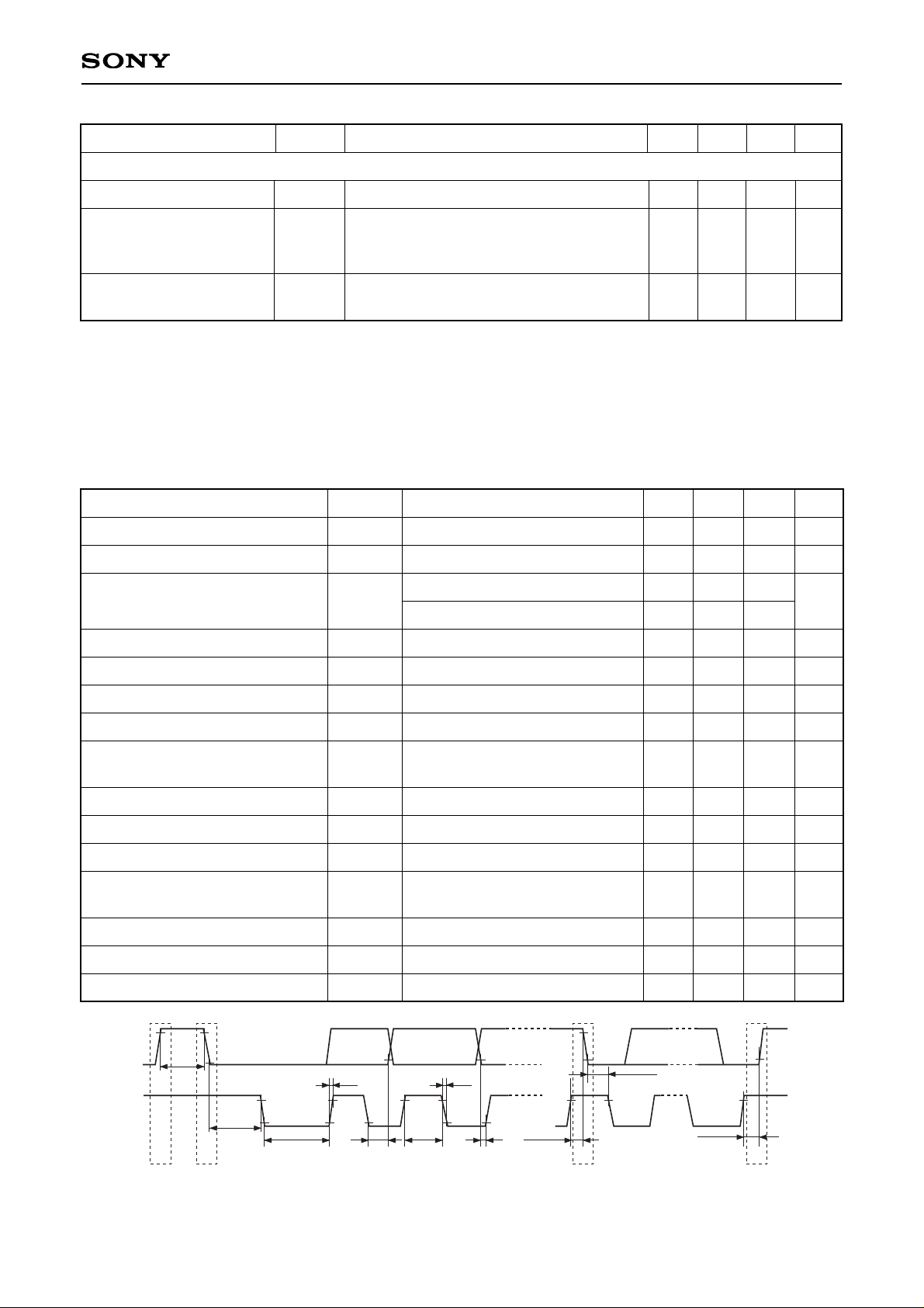
Rin1 + Lin1
Rin1 + Lin1
Rin2, 3, 4 or
Lin2, 3, 4
Rin1 + Lin1
Rin2 + Lin2
Rin3 + Lin3
Rin4 + Lin4
Rin2, 3, 4
Lin2, 3, 4
Rin2 + Lin2
Rin3 + Lin3
Rin4 + Lin4
Rin3
Lin3
Audio frequency response
Frequency bandwidth
Distortion
Input dynamic range
Rin1, 2, 3, 4/Lin1, 2, 3, 4
Cross talk
(Channel separation)
DC offset
Input impedance
Rin1, 2, 3, 4/Lin1, 2, 3, 4
Output impedance
Phase difference
S/N ratio
GVA6
GVA7
GVA9
GVA8
GVA10
GVA11
GVA12
GVA13
GVA14
FAF
FBWA1
THD
VdA1
VctA
Voff
Zin1
Zout
Vpda
S/NA
–0.5
–0.5
–0.5
–0.5
–0.5
–0.5
–0.5
–5.5
–0.5
–0.3
—
—
2.5
—
–30
—
—
—
80
0
0
0
0
0
0
0
–5
0
0
1
0.005
2.9
—
0
120
10
0.05
93
0.5
0.5
0.5
0.5
0.5
0.5
0.5
–4.5
0.5
0.3
—
0.2
—
–76
30
—
—
—
—
dB
dB
dB
dB
dB
dB
dB
dB
dB
dB
MHz
%
Vrms
dB
mV
kΩ
Ω
deg
dB
Item Symbol
Conditions
Min. Typ. Max. Unit
f = 1kHz, 0.5Vrms stereo input. TV volume
set to 0dB, RIN_1/LIN_1 amplifier = –6dB.
TV mono switch on. (Fig. 4)
f = 1kHz, 1Vrms stereo input. TV volume
set to 0dB, RIN_1/LIN_1 amplifier = –6dB.
(Note 1) (Fig. 4)
f = 1kHz, 1Vrms input, TV volume set to
0dB (Fig. 4)
f = 1kHz, 1Vrms stereo input. RIN_1/LIN_1
amplifier = –6dB. VCR mono switch on.
(Fig 4)
f = 1kHz, 1Vrms stereo input. TV volume
set to 0dB (Note 2) (Fig 4)
f = 1kHz, 1Vrms input (Fig 4)
f = 1kHz, 1Vrms stereo input. VCR mono
switch on. (Fig 4)
f = 1kHz, 1Vrms input, Lin3 has no signal
Audio overlay enabled with –11dB
attenuation at input RIN_3 (Fig 4)
f = 1kHz, 1Vrms input
Audio overlay enabled. (Fig 4)
0.3Vp-p input. Output/input gain at 30kHz
with 1kHz serving as 0dB (Fig 4)
0.3Vp-p input; frequency where output
level is –3dB with 1kHz serving as 0dB.
No load attached (Fig 4)
f = 1kHz, 0.5Vrms, unweighted response;
LPF@400Hz, HPF@80kHz (Fig 4)
f = 1kHz, RIN_1/LIN_1 input amplifier set
to –6dB. Dual supply mode used. (Fig 4)
f = 1kHz, 1Vrms input on one input,
measure on any other audio output (Fig 4)
Offset voltage between input and output
(excluding any external series resistor)
(excluding any external series resistor)
f = 1kHz, 1Vrms input to two channels.
Phase difference of stereo output measured
f = 1kHz, 1Vrms input (at 0dB volume).
HPF@20Hz, LPF@20kHz. (Fig 4)
TV
(mono mix)
MONO
TV or
Phono
VCR
(mono mix)
MONO
VCR
VCR
(mono mix)
RTV,
ROUT1,
Phono_R
LTV,
LOUT1,
Phono_L
Note 1) Mono switch set to mix of Rin1 & Lin1 inputs.
Note 2) Mono switch set to mix of RTV & LTV after volume control.
Page 12
– 12 –
CXA2161R
Electronic Volume Control
Volume attenuation step
Mute
TV I/P MUTE or
VCR I/P MUTE
Audio limiter level
AEVC
Amute
Alimit
1.6
—
—
2
–90
6.5
2.4
–76
—
dB
dB
Vp-p
Item Symbol
Conditions
Min. Typ. Max. Unit
f = 1kHz, 0.5Vrms input. Set by I2C (Fig 4)
f = 1kHz, 1Vrms input (Fig 4)
f = 1kHz, 2.5Vrms input. Measure TVp-p
output with limiter switched on. (Fig 4)
Digital Characteristics
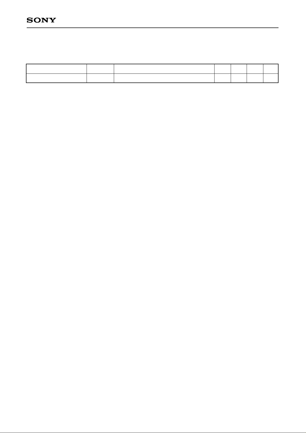
I2C Interface
The I2C interface is compliant with Philips I2C Fast Mode specification (date April 1995). The interface is also
capable of interfacing to +3.3V or +5V logic levels.
SymbolItem Condition Min. Typ. Max. Unit
VIH
VIL
VOL
VHYST
tSP
tF
tSCL
tBUF
tHD;STA
tLOW
tHIGH
tSU;SDA
tHD;DAT
tSU;DAT
tSU;STO
High level input voltage
Low level input voltage
Low level output voltage
Hysteresis of schmitt trigger input
Spike suppression
Fall time for SDA line
SCL clock frequency
Bus free time between a stop and
start
Hold time (repeated start condition)
Low period of SCL clock
High period of SCL clock
Setup time for a repeated start
condition
Data hold time
Data setup time
Setup time for stop condition
With SDA, 3mA current supplied
With SDA, 6mA current supplied
VIH – VIL
400pF bus load
I2C Bus line requirement
I2C Bus line requirement
I2C Bus line requirement
I2C Bus line requirement
I2C Bus line requirement
I2C Bus line requirement
I2C Bus line requirement
I2C Bus line requirement
I2C Bus line requirement
2.3
0
0
0
—
—
—
0
1.3
0.6
1.3
0.6
0.6
0
100
0.6
—
—
—
—
0.5
—
—
—
—
—
—
—
—
—
—
—
5.5
1.5
0.4
0.6
—
50
300
400
—
—
—
—
—
0.9
—
—
V
V
V
V
ns
ns
kHz
µs
µs
µs
µs
µs
µs
ns
µs
tBUF
tHD;STA
SP
tLOW
tR
tHIGH tSU;DAT
tSU;STA
tSU;DAT
P
Sr
tSU;STO
tF
tHD;STA
Page 13
– 13 –
CXA2161R
Logic/Interrupt Output
These outputs are open collector type and normally connected to +5V through a 10kΩ resistor.
Output low voltage DIGVOUTL — 0.15 0.4 V
Item Symbol
Conditions
Min. Typ. Max. Unit
IOL = 1mA
Page 14

– 14 –
CXA2161R
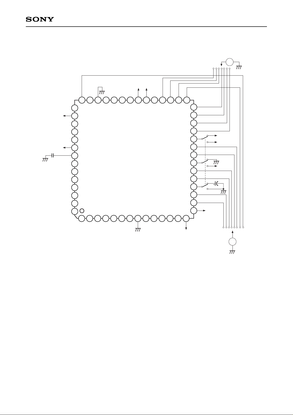
Fig. 1. Video System (DC Test)
DC measured from Pins 1, 3, 4, 5, 6, 7, 38, 39, 41, 43, 45, 46, 47, 50, 51, 52, 53, 54, 55, 56
Notes) 1. All supplies de-coupled close to supply pins 14, 15, 24, 44, 48 with 10nF and 10µF capacitors.
2. All video outputs are unloaded during tests.
75Ω 100nF
75Ω 100nF
75Ω 100nF
75Ω 100nF
75Ω 100nF
75Ω 100nF
75Ω 100nF
100nF
75Ω
68kΩ
+5V
75Ω
100nF
100nF
100nF
75Ω 100nF
75Ω 100nF
75Ω 100nF
75Ω 100nF
+5V
+5V
+12V
+12V
1µF
+5V
V
I2C
SCL SDA
Output
Measurement
Point
Input
Measurement
Point
2 3 4 5 6 7 8 9 11 12 13 14
15
16
17
18
19
21
22
23
24
25
26
27
28
293132333435363738394142
43
44
45
46
47
48
49
50
51
52
53
54
55
56
10
20
3040
1
V
Page 15

– 15 –
CXA2161R
Fig. 2. Video System
(Gain, Dynamic Range, Bandwidth, Differential Gain, Differential Phase, Crosstalk, Linearity,
Sync Detection)
Signal applied to Pins 1, 3, 4, 5, 6, 7, 50, 51, 52, 53, 54, 55, 56
Output signal measured from Pins 38, 39, 41, 43, 45, 46, 47
Notes) 1. All supplies de-coupled close to supply pins 14, 15, 24, 44, 48 with 10nF and 10µF capacitors.
2. For tests requiring video measuring equipment with 75Ω input impedance, an external video line
driver or buffer is used.
3. For video crosstalk tests all video inputs are terminated with 37.5Ω
75Ω 100nF
75Ω 100nF
75Ω 100nF
75Ω 100nF
75Ω 100nF
75Ω 100nF
75Ω 100nF
100nF
75Ω
75Ω
68kΩ
+5V
100nF
100nF 100nF
75Ω
100nF
75Ω
100nF
75Ω
100nF
75Ω
100nF
+5V
+5V
+12V
+12V
1µF
+5V
V
I2C
SCL SDA
Measurement
Point
Input
Signal
2 3 4 5 6 7 8 9 11 12 13 14
15
16
17
18
19
21
22
23
24
25
26
27
28
293132333435363738394142
43
44
45
46
47
48
49
50
51
52
53
54
55
56
10
20
3040
1
22kΩ
150Ω
150Ω
150Ω
150Ω
150Ω
150Ω
Page 16
– 16 –
CXA2161R
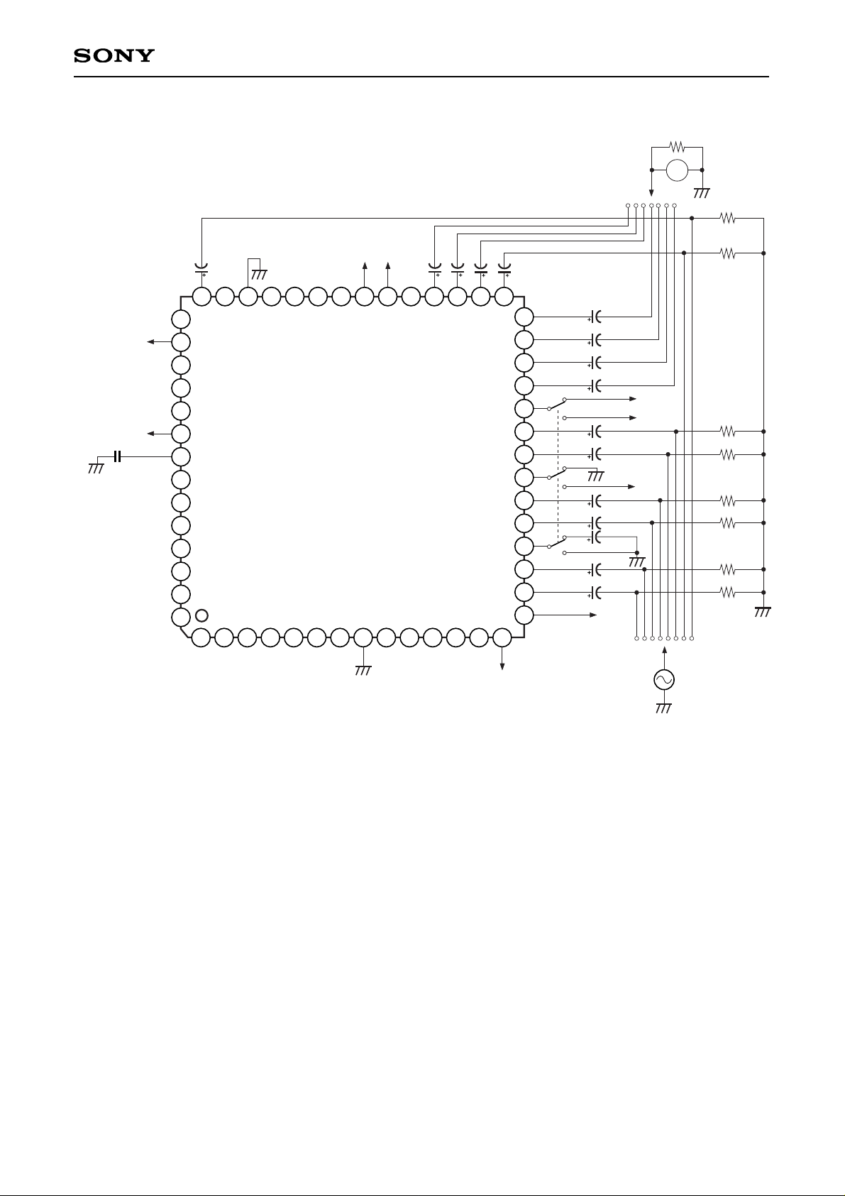
Fig. 3. Audio System (DC Tests)
DC measured from Pins 16, 17, 19, 20, 22, 23, 25, 26, 27, 28, 29, 30, 31, 32, 42
Notes) 1. Single audio supply configuration shown. Operate switches for dual supply configuration.
2. All supplies de-coupled close to supply pins 14, 15, 21, 24, 44, 48 with 10nF and 10µF capacitors.
–5V
100nF
+5V
+5V
+12V
+5V
+12V
1µF
+5V
V
I2C
SCL SDA
Output
Measurement
Point
Input
Measurement
Point
2 3 4 5 6 7 8 9 11 12 13 14
15
16
17
18
19
21
22
23
24
25
26
27
28
293132333435363738394142
43
44
45
46
47
48
49
50
51
52
53
54
55
56
10
20
3040
1
V
Page 17
– 17 –
CXA2161R
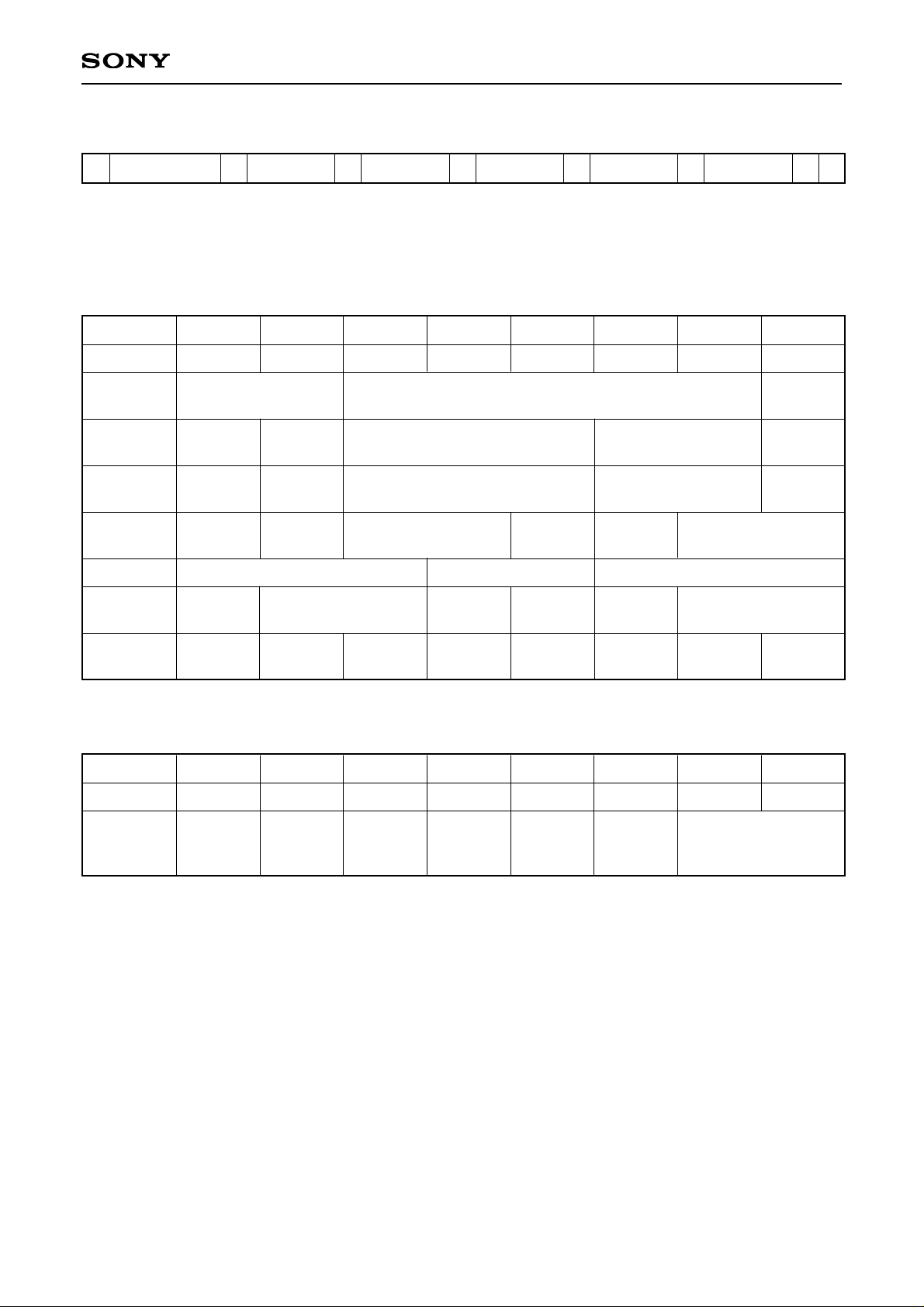
Fig. 4. Audio System
(Single Supply — Gain, Bandwidth, Signal to Noise, Electronic Volume, Zero Cross Detection, Limiter)
(Dual Supply — Distortion, Dynamic Range, Crosstalk)
Signal applied to Pins 16, 17, 19, 20, 22, 23, 29, 42
Output signal measured from Pins 25, 26, 27, 28, 30, 31, 32
Notes) 1. Single audio supply configuration shown. Operate switches for dual supply configuration.
2. All supplies de-coupled close to supply pins 14, 15, 21, 24, 44, 48 with 10nF and 10µF capacitors.
–5V
100nF
+5V
+5V
+12V
+5V
+12V
1µF
+5V
V
I2C
SCL SDA
Measurement
Point
Input
Signal
2 3 4 5 6 7 8 9 11 12 13 14
15
16
17
18
19
21
22
23
24
25
26
27
28
293132333435363738394142
43
44
45
46
47
48
49
50
51
52
53
54
55
56
10
20
3040
1
10µF
1µF
10µF
10µF
1µF
10µF
10µF
10µF
10µF
1µF
1µF
1µF
1µF
1µF
1µF
10kΩ
1kΩ
1kΩ
1kΩ
1kΩ
1kΩ
1kΩ
1kΩ
1kΩ
Page 18
– 18 –
CXA2161R
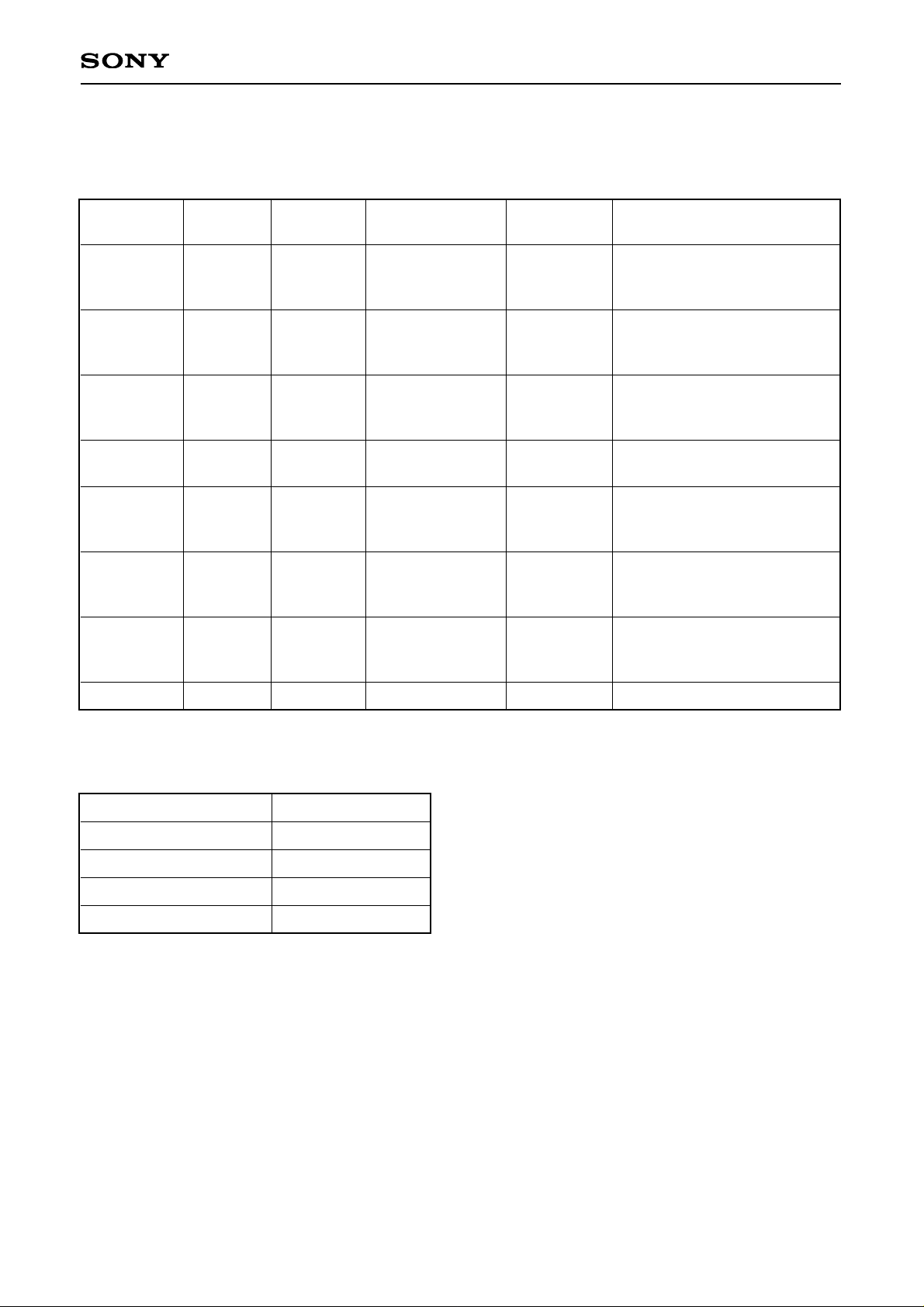
I2C Control Data Format
Slave address A DATA1 A DATA2 A DATA3 A DATA4 A DATAn A PS
S: Start condition A: Acknowledge P: Stop condition
Address = 90H
I2C Data Structure (write mode)
Address
Data1
Data2
Data3
Data4
Data5
Data6
Data7
b7
1
RIN1/LIN1
GAIN CONTROL
MONO
SWITCH
TV AUD
MUTE
TV INPUT
MUTE
TV VOL
BYPASS
OUTPUT
LIMIT
LOGIC
LEVEL
TV MONO SWITCH
VCR MONO SWITCH
FNC LEVEL
VCR VIDEO SWITCH
VCR INPUT
MUTE
SYNC SEL
VIN5
CLAMP
VIN7
CLAMP
VIN3
CLAMP
MIXER
CONTROL
ZCD
VOUT5
0V
ENABLE
VOUT6
ENABLE
VOUT5
ENABLE
VOUT4
ENABLE
VOUT3
ENABLE
VOUT2
ENABLE
VOUT1
RGB GAIN TV VIDEO SWITCH
FNC
FOLLOW
FNC
DIR
FAST BLANK
TV AUDIO SELECT
VCR AUDIO SELECT
b6
0
b5
0
VOLUME CONTROL
b4
1
b3
0
b2
0
b1
0
b0
0 = Write
TV AUD
MUTE
PHONO
BYPASS
OVERLAY
ENABLE
Address
Data
b7
1
NOT
USED
NOT
USED
ZERO
CROSS
STATUS
P.O.D.
NOT
USED
SYNC
DETECT
FNC_VCR
b6
0
b5
0
b4
1
b3
0
b2
0
b1
0
b0
1 = Read
I2C Data Structure (read mode)
Note) ZCD = Zero Cross Detect
P.O.D. = Power on Detect
Page 19
– 19 –
CXA2161R
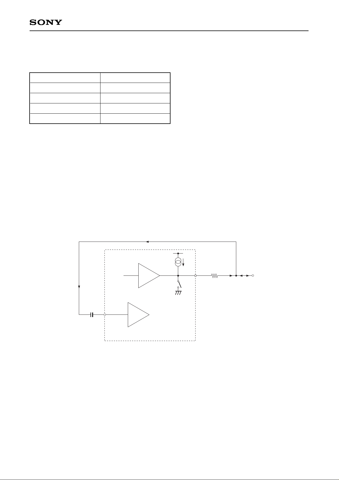
Video I2C Write Structure
Video Switch 1: TV Output [Data 5 Bits 0, 1, 2]
Switch setting
Blue
Vout1
Green
Vout2
R/C
Vout3
CVBS/Y
Vout4
Comment
0 xxxxx000
1 xxxxx001
2 xxxxx010
3 xxxxx011
4 xxxxx100
5 xxxxx101
6 xxxxx110
7 xxxxx111
Encoder
Blue
VIN1
Bias
VCR Blue
VIN2
Bias
Bias
Encoder
Blue
VIN1
Bias
Bias
Encoder
Green
VIN3
Bias
VCR Green
VIN4
Bias
Bias
Encoder
Green
VIN3
Bias
Bias
Encoder
Red
VIN5
Encoder
Chrominance
VIN6
VCR
Chrominance/Red
VIN7
Bias
Encoder
Chrominance
VIN5
Encoder
Red
VIN5
Aux
Chrominance
VIN13
Bias
Encoder
CVBS
VIN8
Encoder
Luminance
VIN9
VCR CVBS/Y
VIN10
TV CVBS
VIN11
Encoder
Luminance
VIN3
Aux
CVBS
VIN12
Aux
CVBS/Y
VIN12
Bias
Digital encoder RGB or
CVBS
Digital encoder Y/C
VCR Y/C or RGB
TV
Digital encoder Y/C
Encoder RGB and Aux CVBS
Aux Y/C or CVBS
Video mute (Power on default)
After power on all TV outputs are off (high impedance output) and muted.
TV RGB GAIN Control [Data 5 Bits 3, 4]
I2C setting RGB GAIN Extra gain/dB
0 xxx00xxx
1 xxx01xxx
2 xxx10xxx
3 xxx11xxx
0 (Power on default)
+1
+2
+3
Page 20

– 20 –
CXA2161R
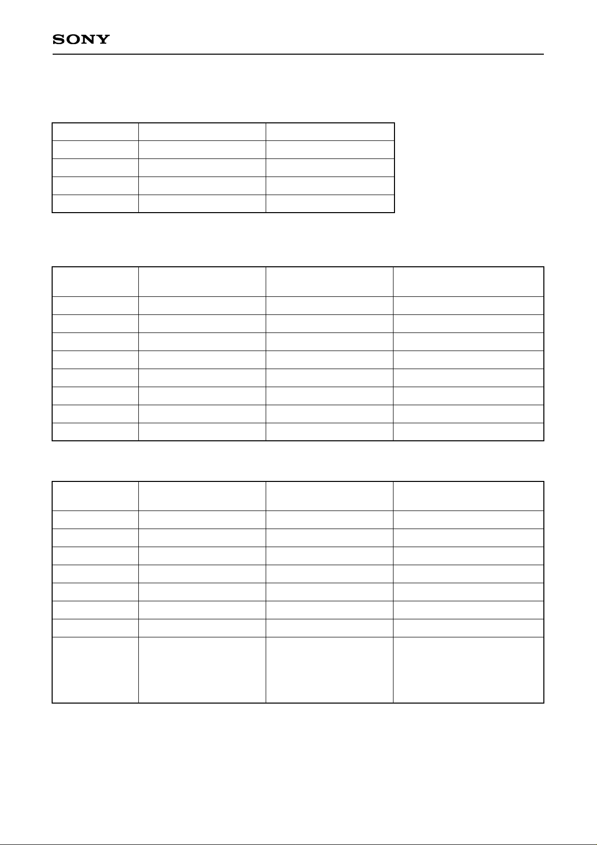
Video Switch 2: VCR Output [Data 5 Bits 5, 6, 7]
Switch setting
Chrominance
Vout5
CVBS/Y
Vout6
Comment
0 000xxxxx
1 001xxxxx
2 010xxxxx
3 011xxxxx
4 100xxxxx
5 101xxxxx
6 110xxxxx
7 111xxxxx
Encoder Chrominance
VIN5
Encoder Chrominance
VIN6
VCR Chrominance
VIN7
Bias
Encoder Chrominance
VIN5
Bias
Aux Chrominance
VIN13
Bias
Encoder CVBS/Y
VIN8
Encoder CVBS/Y
VIN9
VCR CVBS/Y
VIN10
TV CVBS
VIN11
Encoder Luminance
VIN3
Aux CVBS
VIN12
Aux CVBS/Y
VIN12
Bias
Digital encoder Y/C
Digital encoder Y/C or CVBS
VCR Y/C
TV CVBS
Encoder Y/C
Aux CVBS
Aux Y/C or CVBS
Video mute (Power on default)
After power on VCR outputs are off (high impedance) and muted.
MIXER CONTROL [Data 6 Bits 0, 1]
I2C setting
Mixer Output Vout7
0 xxxxxx00
1 xxxxxx01
2 xxxxxx10
3 xxxxxx11
No mix, Vout7 = Vout4 (CVBS)
Mix of Vout4 (Y) + Vout3 (C)
No mix, Vout7 = Vin8 (CVBS)
No mix, Vout7 = Vout4 (CVBS)
(Power on default)
Input Clamp Control VIN3 Clamp [Data 6 Bit 2]
xxxxx0xx = GREEN input on VIN3. DC restore clamp active. (Power on default.)
xxxxx1xx = CVBS input on VIN3. Sync tip clamp active.
Input Clamp Control VIN7 Clamp [Data 6 Bit 3]
xxxx0xxx = CHROMINANCE input on VIN7. Chrominance bias applied. (Power on default.)
xxxx1xxx = RED input on VIN7. DC restore clamp applied.
Input Clamp Control VIN5 Clamp [Data 6 Bit 4]
xxx0xxxx = RED input on VIN5. DC restore clamp applied. (Power on default.)
xxx1xxxx = CHROMINANCE input on VIN5. Chrominance bias applied.
Page 21
– 21 –
CXA2161R
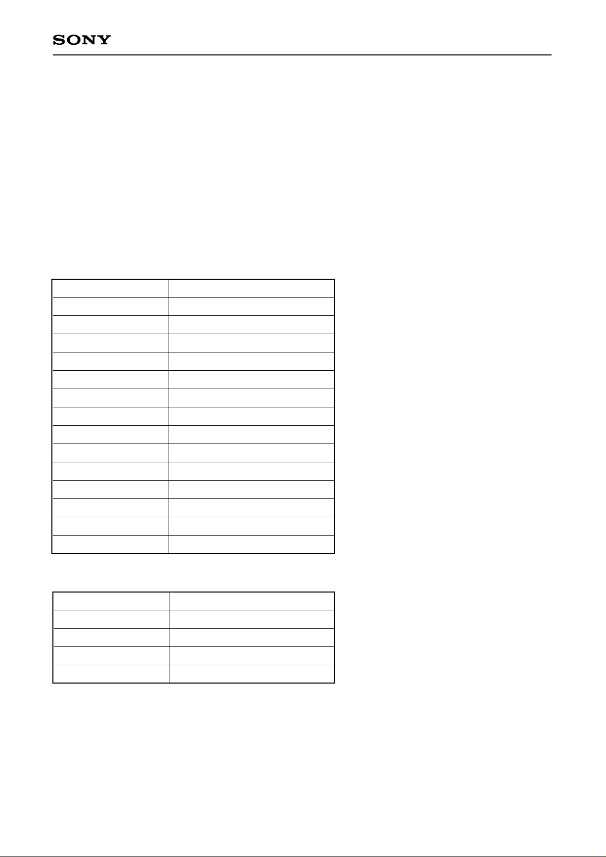
Sync Select Control for RGB DC Restore Circuits SYNC_SEL [Data 6 Bits 5, 6]
When the TV output is set to RGB + Y/CVBS mode. Then it is necessary to select the input that contains the
sync information for the RGB signal. This will normally be the digital encoder CVBS or VCR CVBS input.
I2C setting SYNC SEL Input with sync
0 x00xxxxx
1 x01xxxxx
2 x10xxxxx
3 x11xxxxx
VIN8 (Power on default)
VIN9
VIN10
VIN12
Standby Mode Control [Data 7 Bits 0, 1, 2, 3, 4, 5]
The video outputs VOUT1, 2, 3, 4, 5, 6 can be individually turned off using data byte 7.
0 = Video output off. (Power on default)
1 = Video output on.
Note) When switched off, the video outputs are in a high impedance state. With a normal 150Ω load, the
outputs will be pulled to 0V.
Bi-directional Line Control on VCR Scart. Vout5_0V [Data 7 Bit 6]
x0xxxxxx = Vout5 active. Connected to input specified in VCR switch table.
x1xxxxxx = Vout5 set to 0V (Power on default)
6dB
Vout5
0V
VCR Scart
Pin 15
Red in
Chrominance In
Chrominance Out
Vout5
Chrominance out
Red in
Chrominance in
VIN_7
I = 6mA
(When set to 0V mode)
75Ω
Fig 5. Bi-directional Line to VCR
As Pin 15 on the VCR scart can be bi-directional, either chrominance output or red/chrominance input, it is
necessary for output Vout5 to be individually controlled. When the VCR inputs red/chrominance signals, the
output Vout5 is set to 0V giving the required line impedance of 75Ω.
Page 22
– 22 –
CXA2161R
I2C Audio Signal Control
Channel Select TV (Phono), VCR [Data 2, 3 Bits 1, 2]
Switch setting
RTV, Phono_R, ROUT1
LTV, Phono_L, LOUT1
0 xxxxx00x
1 xxxxx01x
2 xxxxx10x
3 xxxxx11x
Rin1
Rin2
Rin3
Rin4
Lin1
Lin2
Lin3
Lin4
After power on Rin4/Lin4 are selected.
Mono Switch TV [Data 2 Bits 3, 4, 5]
Switch setting
Connection to R channel
output
Connection to L channel
output
0 xx000xxx
1 xx001xxx
2 xx010xxx
3 xx011xxx
4 xx100xxx
5 xx101xxx
6 xx110xxx
7 xx111xxx
R
(R + L mix)
L
R
L
R
R
R
L
(R + L mix)
R
R
L
L
L
L
Comment
Normal
Mono mix
Channel swap
Right channel only
Left channel only
Normal
Normal
Normal (power on default)
Mono Switch VCR [Data 3 Bits 3, 4, 5]
Switch setting
Connection to R channel
output
Connection to L channel
output
0 xx000xxx
1 xx001xxx
2 xx010xxx
3 xx011xxx
4 xx100xxx
5 xx101xxx
6 xx110xxx
7 xx111xxx
R
(R + L mix)
L
R
L
R
R
X
L
(R + L mix)
R
R
L
L
L
X
Comment
Normal
Mono mix
Channel swap
Right channel only
Left channel only
Normal
Normal
All audio outputs disabled
(RTV, LTV, PHONO_R,
PHONO_L, MONO, ROUT1,
LOUT1)
(power on default)
Page 23
– 23 –
CXA2161R
PHONO BYPASS [Data 2 Bit 0]
xxxxxxx0 = Phono outputs connected after volume control block. (Power on default)
xxxxxxx1 = Phono outputs connected before volume control block.
TV VOL BYPASS [Data 2 Bit 6]
x0xxxxxx = TV outputs connected after volume control block. (Power on default)
x1xxxxxx = TV outputs connected before volume control block.
MONO SWITCH [Data 2 Bit 7]
0xxxxxxx = Mono output connected to mix of TV R + L channels. (Power on default)
1xxxxxxx = Mono output connected to mix of RIN1 + LIN1 inputs.
VOLUME CONTROL [Data 1 Bits 1, 2, 3, 4, 5]
Setting
Volume gain
0 xx00000x
1 xx00001x
2 xx00010x
3 xx00011x
4 xx00100x
5 xx00101x
6 xx00110x
7 xx00111x
8 xx01000x
9 xx01001x
10 xx01010x
11 xx01011x
:
31 xx11111x
+6dB
+4dB
+2dB
0dB (power on default)
–2dB
–4dB
–6dB
–8dB
–10dB
–12dB
–14dB
–16dB
:
–56dB
AUDIO RIN1/LIN1 GAIN [Data 1 Bits 6, 7]
Setting
Input attenuation
0 00xxxxxx
1 01xxxxxx
2 10xxxxxx
3 11xxxxxx
–6dB (Power on default) (Note 1)
–3dB
+0dB
+3dB
Note 1) The power on default is –6dB. As the output amplifiers have a nominal +6dB gain the overall input to
output gain is 0dB.
Page 24
– 24 –
CXA2161R
OVERLAY ENABLE [Data3 Bit 0]
xxxxxxx0 = Overlay off (Power on default)
xxxxxxx1 = Overlay on: Rin3 and Lin3 are mixed and added to Rin1, Lin1 channels. Rin1 and Lin1 are attenuated
by 16dB before mixing with the tone.
TV Mute and Zero Cross Operation
When the zero cross is switched on (ZCD = 1), volume control changes are only implemented when the audio
signal passes though the zero cross point. Similarly, when a mute instruction is sent, the TV outputs are only
muted when the signal passes the zero cross point. This eliminates any click noise.
There are two TV audio mute control bits in the bus map. By having two bits it allows the TV outputs to be muted,
the TV channel changed and then un-muted all in one I2C write operation. The normal structure for a click free
audio channel change is as follows:
Data 1: Mute the TV audio output with the ZCD switched on.
Data 2: Change the TV audio source.
Data 3: Un-mute the TV audio output again with the ZCD switched on.
Operation of the Mute circuit
TV Aud Mute [Data 1 Bit 0]
[Data 3 Bit 7]
ZCD [Data 7 Bit 7] TV, Phono and Mono output
0
0
1
1
0
1
0
1
Un-mute immediately
Un-mute on next zero cross
Mute immediately
Mute on next zero cross
After power on TV Audio Mute = 1 and ZCD are set to 1.
TV INPUT MUTE [Data 4 Bit 7]
0xxxxxxx = The input to the TV switch is not muted.
1xxxxxxx = The input to the TV switch is muted. (power on default)
VCR INPUT MUTE [Data 6 Bit 7]
0xxxxxxx = The input to the VCR switch is not muted.
1xxxxxxx = The input to the VCR switch is muted. (power on default)
OUTPUT LIMIT [Data 3 Bit 6]
This will limit the output level of the volume control block to 2.2Vrms maximum.
0xxxxxxx = The volume control outputs are not limited. (power on default)
1xxxxxxx = The volume control outputs are limited to 2.2Vrms.
Page 25

– 25 –
CXA2161R
Fast Blanking Operation (Pin 16 on SCART), FBLK
The fast blanking signal instructs the TV to select either the external CVBS information or the external RGB
information. This is used to superimpose an on screen display (OSD) presentation (normally RGB) upon a
CVBS background. Fast blanking information has the same nominal phase as the RGB and CVBS signal, and
is defined as follows,
Fast blanking output at scart,
1. CVBS mode: Scart pin voltage = 0 to 0.4V
2. RGB mode: Scart pin voltage = 1 to 3.0V
The threshold voltage is approximately 0.75V at the scart input.
Fast Blanking I2C Control
In the CXA2161R, there are two fast blanking inputs, one associated with the digital encoder input (FBLK_IN1)
and another associated with the VCR RGB/CVBS input (FBLK_IN2). These can be selected and switched to the
output using an I2C instruction. In addition, the fast blank output pin can be set to a constant 0V or +3.5V by
means of the I2C control. Hence there are four possible states. These are set according to the following table.
FAST_BLANK [Data 4 Bits 0, 1]
I2C setting BLANK_LEVEL
Fast blank output pin voltage
0 xxxxxx00
1 xxxxxx01
2 xxxxxx10
3 xxxxxx11
0V (Power on default)
Same level as Fast Blank in 1 (0/+3.5V)
Same level as Fast Blank in 2 (0/+3.5V)
+3.5V
Fast Blank Output Interface
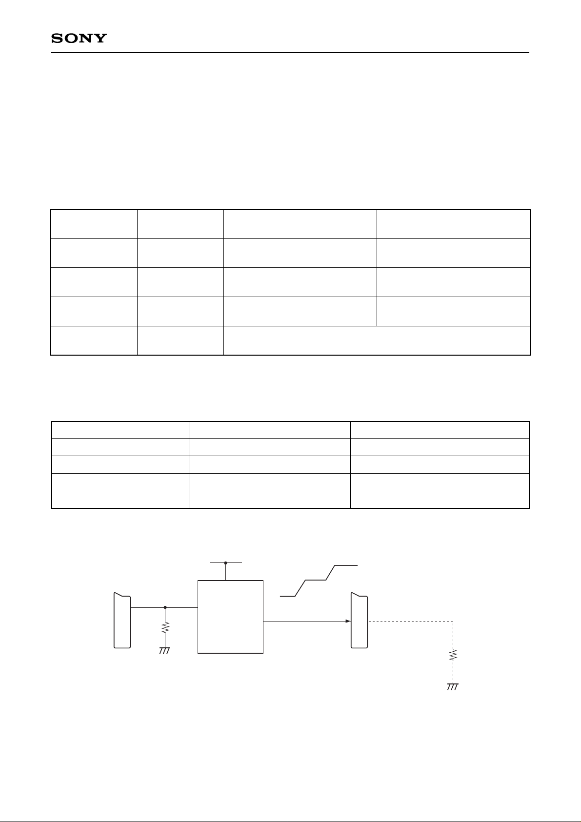
The Fast Blanking output pin is connected to the scart via a 75Ω resistor.
TV_FBLK
0V/+3.5V
75Ω
75Ω
Scart line 16
TV
CXA2161R
Fig. 6. Fast Blanking Output Interface
Page 26
– 26 –
CXA2161R
Function Switching Operation (Pin 8 on scart)
The function switch facility is designed to read the status of the SCART function Pin 8 from the VCR scart
connector and store this in the status register. Both, VCR and TV function lines can be set to outputs and
controlled by I2C. The TV function line has two modes, the first being control via I2C and secondly the follow
mode where the output will follow the same state as the VCR input.
Setting the Direction for the Function Lines
The input and control for the function lines is set by the FNC_DIR and FNC_FOLLOW bits.
FNC_FOLLOW
[Data 4 Bit 3]
FNC_DIR
[Data 4 Bit 2]
VCR Pin 8
TV Pin 8
0
0
1
1
0
1
0
1
Input
(Level stored in read register)
Output
Controlled by FNC_LEVEL
Input
(Level stored in read register)
Output
Controlled by FNC_LEVEL
Output
Holds previous level
Output
Follows same level as VCR input
Output
(Both set to same voltage controlled by FNC_LEVEL)
FNC_LEVEL [Data 4 Bits 4, 5]
These bits set the voltage at the (TV_FNC or VCR_FNC) outputs. The output is determined by the table above.
I2C control FNC_LEVEL
Voltage at output
0 xx00xxxx
1 xx01xxxx
2 xx10xxxx
3 xx11xxxx
< 2V
> 4.5V, < 7V
< 2V
> 9.5V
Mode
Internal TV
External scart input 16:9 mode
Internal TV
External scart input 4:3 mode
Note) After power on the output is internal TV mode ie. 0V at the pin.
FNC_VCR
+12V_DIG
Inside TV
< 2V
> 9.5V
> 4.5 < 7V
10kΩ
Scart Pin 8
Scart Pin 8
FNC_TV
10kΩ
Fig. 7. TV Function Switch Output
Page 27

– 27 –
CXA2161R
Logic and Interrupt Output
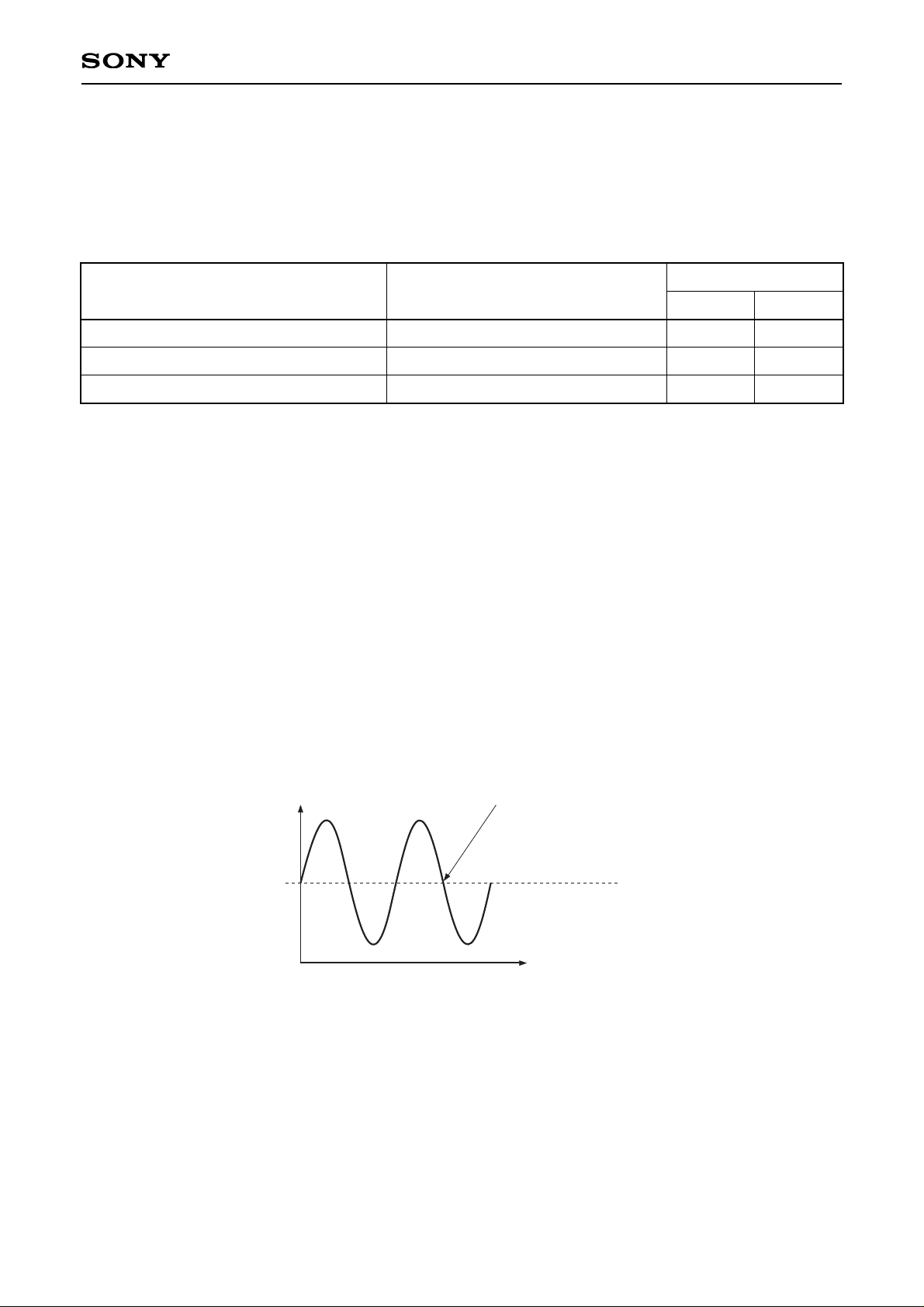
These open collector output pins can be used for an interrupt line to a microprocessor or as a general purpose
logic output.
Interrupt Output
The INTRUPT pin will become a current sink for approximately 2µs when the VCR input function line changes
from:
a) 0 to 6V, 6 to 0V b) 0 to 12V, 12 to 0V c) 6 to 12V, 12 to 6V
This pin will normally be connected to +5V through a 10kΩ resistor.
Logic Output
The logic output level can be changed using the logic output bit in the I2C register, LOGIC_LEVEL.
LOGIC LEVEL [Data 4 Bit 6]
x0xxxxxx = Current sink mode resulting in < 0.4V saturation voltage on logic pin. (Power on default)
x1xxxxxx = Open collector/high output impedance on logic pin.
Imax during current sink = 1mA
External resistors
10kΩ
2µs
To Microprocessor
+3 to 14V
INTRUPT
LOGIC
10kΩ
Fig. 8. INTRUPT and Logic Line Interface
Page 28
– 28 –
CXA2161R
Read Mode Status Register
The following information can be read from the status register:
FNC VCR [Bits 0, 1]
The status register bits 0, 1 hold the level of the input function line
Input pin voltage
FNC_VCR
Data 8
0 to +2V (default)
+4.5 to +7V
+9.5 to +12V
(Internal)
(16:9 External)
(4:3 External)
b1
0
0
1
b0
0
1
1
SYNC DETECT [Bit 2]
Once a valid sync signal is detected on the input selected by SYNC_SELECT this bit is set to 1. The bit is
reset to 0 every time the SYNC_SELECT is changed. It is assumed that when a video input is in-active then
the input level will be 0V with minimum noise.
POD (Power on Detect) [Bit 4]
This bit is set to 1 after power on. It is then changed to 0 after the first I2C read. It is used to detect if the supply
has been corrupted. If the POR bit is read as 1 at any time then the IC should be re-initialized to the correct I2C
settings.
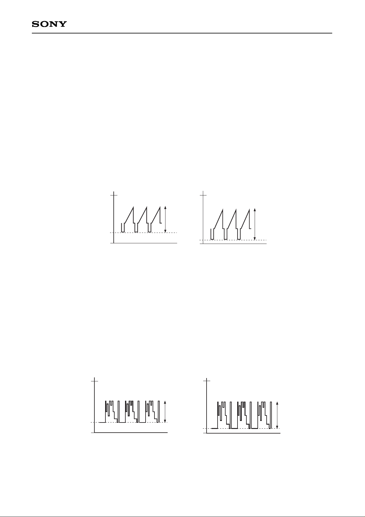
Zero Cross Status [Bit 5]
This audio function is used to determine if an input audio signal has passed the zero cross point. For dual
supply operation the zero cross point is 0V. For Single supply, the zero cross point is approximately 6V.
Input signal
Bias voltage
Zero cross point
Fig. 9. Zero Cross Point
0 = No zero cross detected
1 = Signal has passed through zero cross point.
SCART mode
Page 29
– 29 –
CXA2161R
Description of Operation
Video Section
Inputs and Outputs
The video section comprises of thirteen (13) high impedance inputs switched through to seven (7) video
outputs. An internal +6dB amplifier is connected to each output. The amplifier is required to compensate for the
6dB attenuation that occurs at the 75Ω series output resistor. The outputs VOUT_1 to VOUT_6 are capable of
driving 150Ω loads. Output VOUT_7 is designed to interface to an RF Modulator but requires an external buffer
to drive a 75Ω load.
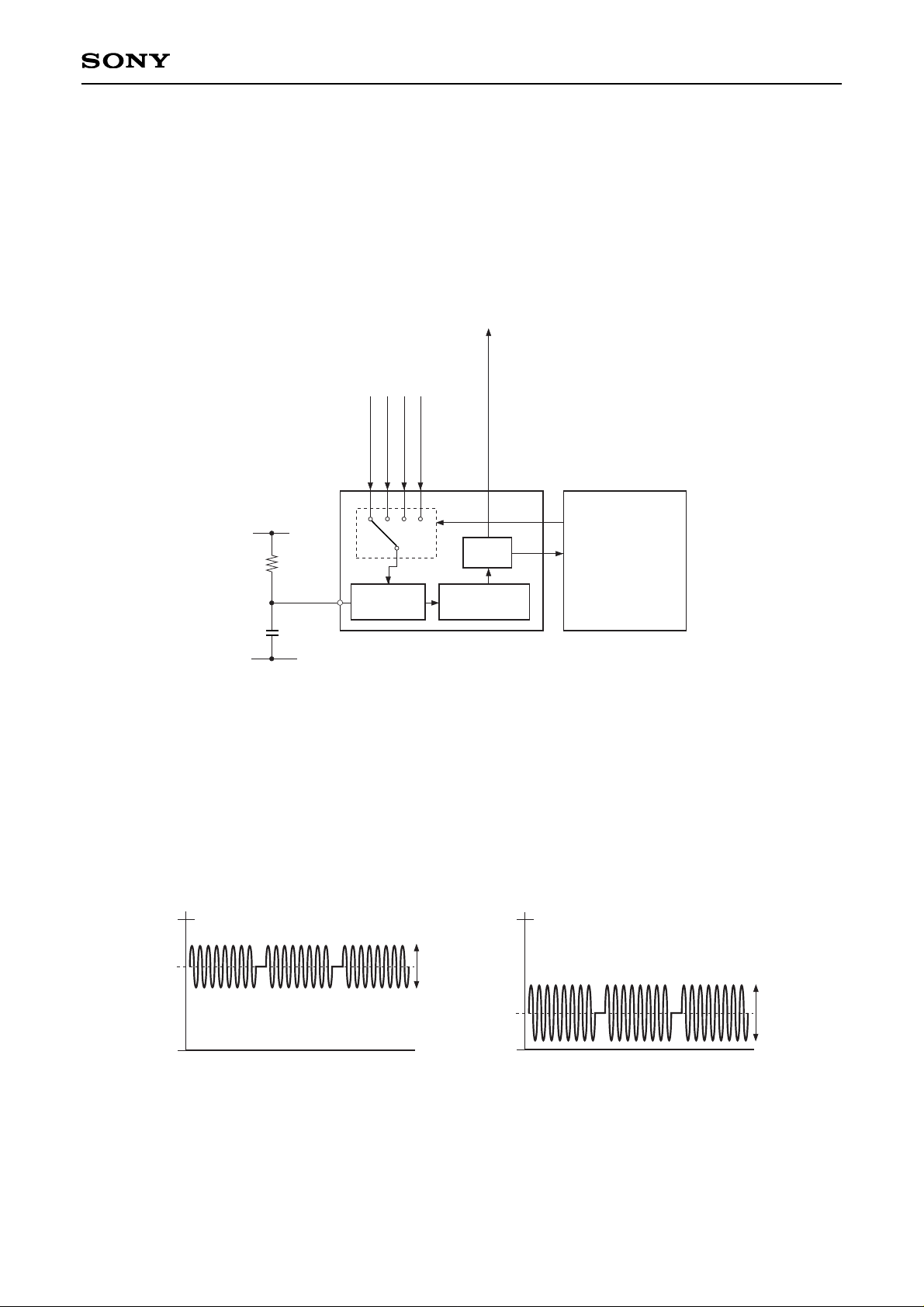
Composite/Luminance Inputs
The 4 composite (or luminance) inputs are ac coupled to the input pins. The signals are first sync tip clamped
to a set level. These clamps are permanently active, therefore these inputs should only be used for signals
with a sync.
2.4V
0V
1Vp-p
VCC = +5V
Input signal
0.3V
0V
2Vp-p
VCC = +5V
Output signal
Fig. 10. CVBS/Y Waveforms
RGB Inputs
The RGB inputs are ac coupled to the input pins. The inputs have a dc restore circuit, which is used to set the
blanking level to a fixed voltage. The clamps are controlled by the timing signal provided by the sync detect
circuit. It is necessary to select the correct luma or CVBS signal associated with the RGB inputs for the sync
select circuit. It is assumed that a sync signal will not be present on any of the RGB input signals. For inputs
that can be either red or chrominance then the clamp can be switched between the dc restore mode (for red
input) and average level bias (for chrominance). The RGB signals are fed through additional amplifiers that
are controlled via I2C. These allow the nominal 0.7Vp-p signal to be increased to 0.8Vp-p, 0.9Vp-p or 1Vp-p.
When the TV output is in Y/C mode, the RGB gain should be set to 0dB to prevent over amplification of the
chrominance output.
2.4V
0V
0.7Vp-p
VCC = +5V
Input signal
0.6V
0V
1.4Vp-p
VCC = +5V
Output signal
Fig. 11. RGB Waveforms
Page 30
– 30 –
CXA2161R
Sync Detection Circuit
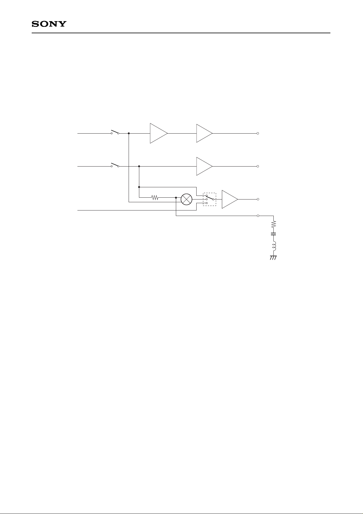
The clamp signals, used to restore the RGB level, are generated from the sync detect circuit. By using the
SYNC_SELECT control bits, the 4 different CVBS/Y inputs may be selected. Once selected, the clamped
signal is compared with a threshold voltage 65mV above the tip level. If the signal is less than this threshold it
is not passed to the next block. If greater than the threshold, it is passed to the discrimination circuit that
checks that the duty cycle is greater than 91%. The discrimination block also contains a time constant which,
when a sync is detected, holds the status line high for at least 11 video lines. If a valid sync signal is detected
the SYNC_DETECT bit in the read register is set to 1.
Comparator
Duty
Discrimination
LOGIC
DIG CVBS/Y
DIG CVBS/Y
VCR CVBS/Y
AUX CVBS/Y
RGB input clamp timing
SYNC_SELECT
Status register
SYNC_DETECT bit
I
2
CSync detect circuit
External R/C
SYNC_ID
GND_VID
+5V_VID
68kΩ
0.1µF
Fig. 12. Sync Detection Circuit
Chrominance Inputs
The chrominance signals are ac coupled to the input pins. The inputs have a fixed dc bias that sets the
average level to approximately 3V for VIN_5 & VIN_7 and 2.35V for VIN_6 & VIN_13. For inputs that can also
be RED signals the input circuit can be switched to the dc restore mode.
Typical waveforms:
2.35 or 3V
0V
0.7Vp-p
VCC = +5V
Chrominance input pin voltage
1.8V
0V
1.4Vp-p
VCC = +5V
Chrominance output pin voltage
Fig. 13. Chrominance Waveforms
Page 31
– 31 –
CXA2161R
Y/C Mixer
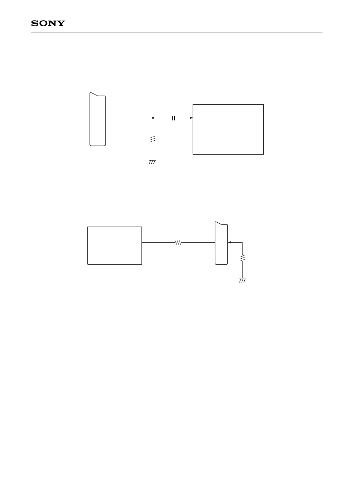
A Y/C mixer can be used for mixing Luminance and Chrominance signals for use with an external RF modulator
connected to VOUT_7. The Y/C mixer is controlled via the I2C data bus. The signal may be a mix of the TV Y/C
signals or simply the TV CVBS signal. It is also possible to select the CVBS signal from the digital encoder.
The circuit is shown in Fig 14. with a trap circuit used to give 6dB attenuation at 4.43MHz of the Luminance
signal. The output VOUT_7 cannot drive loads higher than 20kΩ resistive. If it is necessary to drive a 75Ω
load with this output then an external emitter follower arrangement should be used.
6dB
0, 1, 2
or 3dB
VIN_8 = CVBS
R/C
CVBS/Y
VOUT_3
VOUT_4
VOUT_7
TRAP
Mixer
switch
For recommended values:
see application circuit
6dB
R
C
L
2kΩ
6dB
Fig. 14. Internal Y/C Mixer Circuit
Switching the Video Outputs Off
Each video output can be individually turned off using the I2C. When turned off, the output is set to a high
impedance state and hence the current consumption and power dissipation is reduced. After power on, all the
video outputs are set to the high impedance state.
Page 32
– 32 –
CXA2161R
Typical Video Interface Circuits
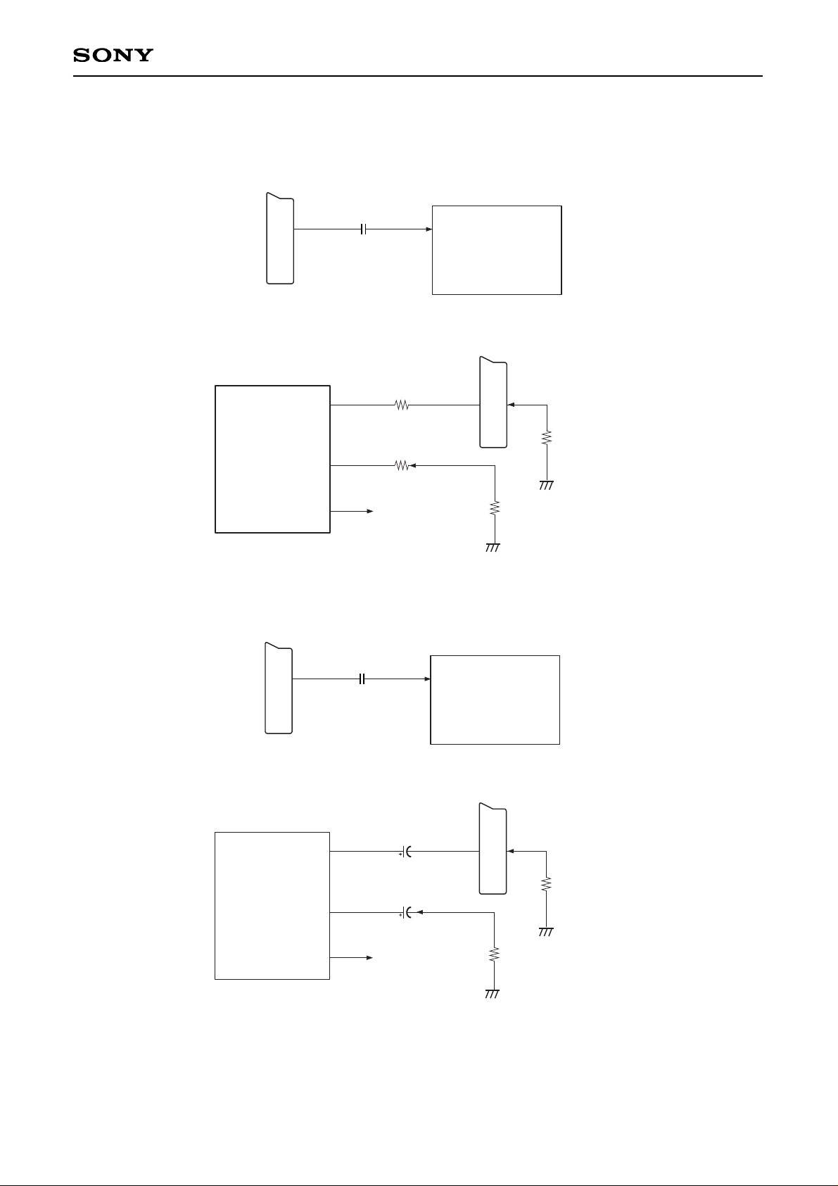
Single or Dual Supply
100nF
75Ω
Scart
VIN_1 to VIN_13
Fig. 15. Video Input Interface
75Ω
(Line C = 400pF max)
75Ω
Scart
VOUT_1 to VOUT_6
Fig. 16. Video Output Interface
Page 33

– 33 –
CXA2161R
Audio Section
Inputs and Outputs
The audio system consists of 4 stereo inputs, 2 stereo outputs and separate mono and Phono outputs. The
stereo outputs can be connected to any one of the 4 stereo inputs. All audio inputs have a –6dB attenuator
except RIN_1 and LIN_1. Therefore, the net gain of the audio system from input to output is 0dB, as an
amplifier having +6dB of gain follows the internal switch. The stereo input RIN_1/LIN_1 has extra switchable
gain as this input is typically connected to an audio DAC with full scale of 1Vrms or less.
The output impedance of each audio amplifier is near zero, and may be directly coupled to the scart in the
case of a dual supply but must be ac coupled through a capacitor (typically 10µF) for the single supply case.
The outputs are capable of driving 600Ω loads. The user may add additional low pass filters to the outputs.
TV Output Switching
The TV audio section is composed of an audio switch followed by a volume control stage. The volume is
adjustable from +6dB to –56dB in 2dB steps. The volume control block includes a switchable limiter function to
prevent the output signals exceeding 2.2Vrms. When activated, the output signals from the volume control
block will be clamped to 2.2Vrms. A mono switch that allows the mixed R + L signal to be switched to the R
and L output channels follows the volume control section. The mono switch is also capable of routing the R
signal onto both R and L channel and similarly the L signal to the R and L output channels. This may be used if
the audio channels consist of two different languages. It is also capable of swapping the R and L channels.
TV Mute
This I2C mute function acts only on the TV, Phono and mono audio circuits. Audio mute will be implemented
after an audio zero cross detection to reduce click noise if ZCD = 1.
Zero Cross Detector (ZCD)
The zero cross detector reduces the effect of click noise when implementing a volume change or an audio
mute. The volume change or mute instruction sent by I2C will only be implemented when a minimal (ie zero
cross) signal amplitude is detected.
It can be seen from the I2C write format that the same mute bit occurs in DATA1 and DATA3. This allows the
software to action a mute, then after a delay (1/Audio_freq (min)) make any suitable changes to the audio
source and then un-mute the output buffer. Such a period provides ample time to allow any audio signals to
pass the zero cross point before the signal source is changed.
VCR Output Switching
The outputs ROUT1, LOUT1 have a fixed gain of 0dB from the input. If any attenuation is required then it is
possible to insert a series resistance on the input. Again, this output has a mono switching block that allows
the mixed R + L to be inserted on both output channels.
Page 34

– 34 –
CXA2161R
Phono outputs
There is a stereo Phono output that carries the same signal as the TV output. This is typically used for
connection to a hi-fi. The signal level of the Phono outputs is normally the same as the TV outputs however it is
possible to bypass the volume section and set the Phono outputs to a fixed level. If any attenuation is required
then this can be done externally.
Mono Output
The mono output for the RF modulator has two settings. The first is a mix of the TV R + L channels. In this
case, the output signal will have the same volume control as the RTV/LTV outputs. The second setting is a mix
of the audio DAC inputs (RIN_1 + LIN_1). In this setting the output will always have fixed volume and if the
tone overlay is used, this will appear on the output.
Audio Overlay
The inputs RIN_3, LIN_3 may be used for a normal stereo audio input or alternatively to overlay an external
audio source onto the TV outputs. This may be a tone or voice. The R and L inputs are mixed and then added
equally to the RIN_1 and LIN_1 inputs. The I2C control bit Audio overlay enable is used to switch on this facility
and control the attenuator block on RIN_3 which is set to give an extra 5dB of attenuation when switched on. If
two tones are used then it is up to the user to switch them individually before the A/V switch. When the tone
overlay is activated, the signals RIN_1, LIN_1 are attenuated by approximately 16dB before mixing.
Audio Disable
All the audio outputs may be disabled using the Audio Output Disable function in the VCR mono switching
block [Data Byte 3 Bits 3, 4, 5 set to 111]. This disable mode is different from the normal mute as it can be
used for power reduction in stand by modes.
Page 35
– 35 –
CXA2161R
Typical Audio Interface Circuits
Supply type 1: Dual supply
Scart
RIN_1, 2, 3, 4
LIN_1, 2, 3, 4
0.1µF
Fig. 17. Audio Input Interface
Scart
To RF modulator
Optional protection
resistor
600Ω to 10kΩ
(Line C = 400pF max)
600Ω to 10kΩ
(Line C = 400pF max)
Optional protection
resistor
RTV, LTV
ROUT1, LOUT1
PHONO_R,
PHONO_L
MONO
Fig. 18. Audio Output Interface
Supply type 2: Single supply
Scart
RIN_1, 2, 3, 4
LIN_1, 2, 3, 4
0.1µF
Fig. 19. Audio Input Interface
Scart
To RF modulator
The user may use larger capacitors if required.
10µF
600Ω to 10kΩ
(Line C = 400pF max)
600Ω to 10kΩ
(Line C = 400pF max)
RTV, LTV
ROUT1, LOUT1
PHONO_R,
PHONO_L
MONO
10µF
Fig. 20. Audio Output Interface
Page 36

– 36 –
CXA2161R
Application in Set Top Box
VIN_1B
BVOUT_1
GVOUT_2
R/CVOUT_3
CVBS/YVOUT_4
TV_FBLK
TV_FNC
FAST BLANKING
FUNCTION SWITCH
CVOUT_5
CVBS/YVOUT_6
CVBSVOUT_7
VIN_3G
VIN_5R
VIN_8CVBS
VIN_6C
VIN_9
FBLK_IN1
Y
FAST BLANKING
VIN_2B
VIN_11CVBS
VIN_12CVBS/Y
VIN_13C
VIN_4G
VIN_7R/C
VIN_10
FBLK_IN2
VCR_FNC
CVBS/Y
FAST BLANKING
FUNCTION SWITCH
Digtal
Encoder
VCR
VCR
RF
MOD.
TV
TV
AUX
Inputs Outputs
CXA2161R
A/V switch
Fig. 21. Video Application with 6 Output Digital Encoder
VIN_1B
BVOUT_1
GVOUT_2
R/CVOUT_3
CVBS/YVOUT_4
TV_FBLK
TV_FNC
FAST BLANKING
FUNCTION SWITCH
CVOUT_5
CVBS/YVOUT_6
CVBSVOUT_7
VIN_3G/CVBS
VIN_5R/C
VIN_8
FBLK_IN1
CVBS/Y
FAST BLANKING
VIN_6
VIN_9
C
CVBS/Y
VIN_2B
VIN_11CVBS
VIN12CVBS/Y
VIN13C
VIN_4G
VIN_7R/C
VIN_10
FBLK_IN2
VCR_FNC
CVBS/Y
FAST BLANKING
FUNCTION SWITCH
Digtal
Encoder
VCR
Analogue
Sat.
VCR
RF
MOD.
TV
TV
AUX
Inputs Outputs
CXA2161R
A/V switch
Fig. 22. Video Application with 4 Output Digital Encoder
Page 37

– 37 –
CXA2161R
Audio Application
STB audio DAC
full scale = 2Vrms
RIN_1
LIN_1
VCR
fs = 2Vrms
RIN_2
LIN_2
TV or
STB generated voice/
tone
RIN_3
LIN_3
AUX
fs = 2Vrms
RIN_4
LIN_4
RTV
LTV
ROUT1
LOUT1
PHONO_R
PHONO_L
TV
(Mono)
MONO
TVL R
VCR
Hi-Fi
RF
Modulator
L R
Fig. 23. Audio Application
Page 38
– 38 –
CXA2161R
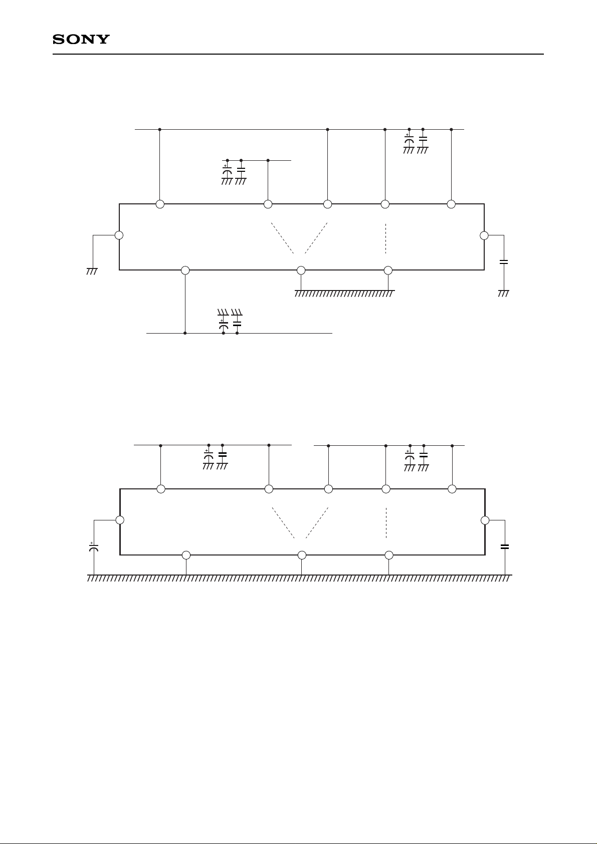
Supply Connections
+12V (±0.6V)
–5V (±0.25V)
+5V (±0.25V)
+5V/12V_VCCA +12V_DIG +5V_DIG +5V_VID
GND_VIDGND_DIG–5V_GNDA
AUD_BIAS
+5V_VOUT
VID_BIAS
0.1µF
Fig. 24. Dual Supply
+12V (±0.6V)
+5V (±0.25V)
+5V/12V_VCCA +12V_DIG +5V_DIG +5V_VID
GND_VIDGND_DIG–5V_GNDA
AUD_BIAS
+5V_VOUT
VID_BIAS
0.1µF
22µF
Fig. 25. Single Ended Supply
Page 39
– 39 –
CXA2161R
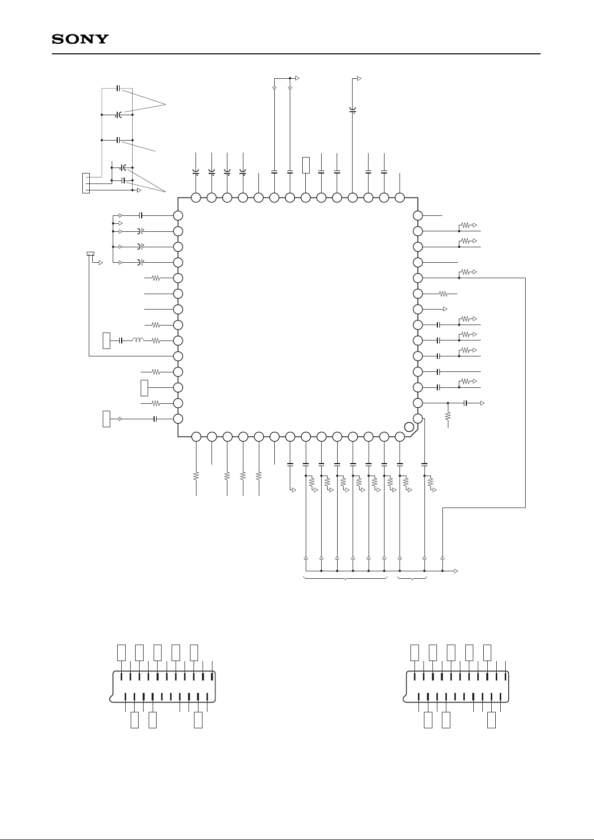
Application Circuit 1
Single Ended Supply
+12V
+5V
TV_FNC
TV_FBLANK
10kΩ
VCR_FNC
+12V
TV_LOUT
VCR_RIN
VCR_LIN
TV_RIN
TV_LIN
TV_ROUT
VCR_LOUT
VCR_ROUT
100nF
100nF
100nF
100nF
100nF
100nF
DIGITAL_AUDIO_R
Digital Audio Input
DIGITAL_AUDIO_L
75Ω
VCR_FBLANK
75Ω
VCR_BLUE
75Ω
75Ω
75Ω
VCR_GREEN
100nF
75Ω
VCR_RED/C
100nF
VCR_CVBS_IN
100nF
75Ω
68kΩ
TV_CVBS_IN
100nF100nF
100nF
+5V
75Ω
100nF
75Ω
100nF
CXA2161R
100nF
DIG_GREEN
DIG_BLUE
75Ω
100nF
DIG_RED
75Ω
100nF
DIG_CHROMA
75Ω
100nF
DIG_CVBS
75Ω
100nF
DIG_LUMA
75Ω
100nF
AUX_Y/CVBS
75Ω
100nF
AUX_C
DIG_FBLANK
GNDGND
GND
TV_CVBS_OUT
VCR_RED/C
VCR_CVBS_OUT
+5V
SCL
SDA
+5V
75Ω
75Ω100nF 75Ω
1.8kΩ
12pF
10kΩ
10kΩ
100nF
TV_RED/C
75Ω
TV_GREEN
75Ω
TV_BLUE
+5V
+5V
75Ω
AUX_L
100µH
10µF100nF
+5V
100nF
10µF
Supplies
100nF
10µF 10µF 10µF
10µF
10µF
10µF
10µF
22µF
TV
21
19
TV_CVBS_OUT
17
15
TV_RED/C
13
11
TV_GREEN
9
7
TV_BLUE
5
3
TV_LOUT1TV_ROUT
20
TV_CVBS_IN
18
16
TV_FBLANK
141210
8
TV_FNC
6
TV_LIN
4
2
TV_RIN
GND
GND
GND
GND
GND
GND
GND
GND
VCR
21
19
VCR_CVBS_OUT
17
15
VCR_RED/C
13
11
VCR_GREEN
9
7
VCR_BLUE
5
3
VCR_LOUT1VCR_ROUT
20
VCR_CVBS_IN
18
16
VCR_FBLANK
141210
8
VCR_FNC
6
VCR_LIN
4
2
VCR_RIN
GND
GND
GND
GND
GND
GND
GND
GND
Digital encoder
inputs
AUX video
inputs
Digital fast
blank
+12V
VOUT_7 to RF Modulator
Place close to Pin 14
Place close to Pin 44
Place close to Pin 24
GND
+5V_VOUT
VOUT_3
VOUT_2
VOUT_1
+5V_VID
VID_BIAS
VIN_1
VIN_3
VIN_5
VIN_6
VIN_8
VIN_9
SYNC_ID
VIN_11
VIN_10
VIN_7
VlN_4
VIN_2
GND_DIG
TV_FBLK
FBLK_IN1
FNC_TV
FBLK_IN2
FNC VCR
VOUT_5
GND_VID
VOUT_6
VOUT_7
TRAP
INTRUPT
SCL
SDA
LOGIC
MONO
PHONO_R
PHONO_L
1 2 3 4 5 6 7 8 9 11 12 13 14
15
16
17
18
19
21
22
23
24
25
26
27
28
293132333435363738394142
43
44
45
46
47
48
49
50
51
52
53
54
55
56
10
20
3040
LOUT1
RTV
LTV
+5V/12V_V
CCA
RIN_1
LIN_1
–5V_GNDA
RIN_2
LIN_2
AUD_BIAS
RIN_3
LIN_3
+5V_
DIG
+12V_
DIG
LlN_4
RIN_4
VIN_13
AUX_R
VIN_12
VOUT_4
ROUT1
Application circuits shown are typical
examples illustrating the operation of
the devices. Sony cannot assume
responsibility for any problems arising
out of the use of these circuits or for
any infringement of third party patent
and other right due to same.
Page 40
– 40 –
CXA2161R
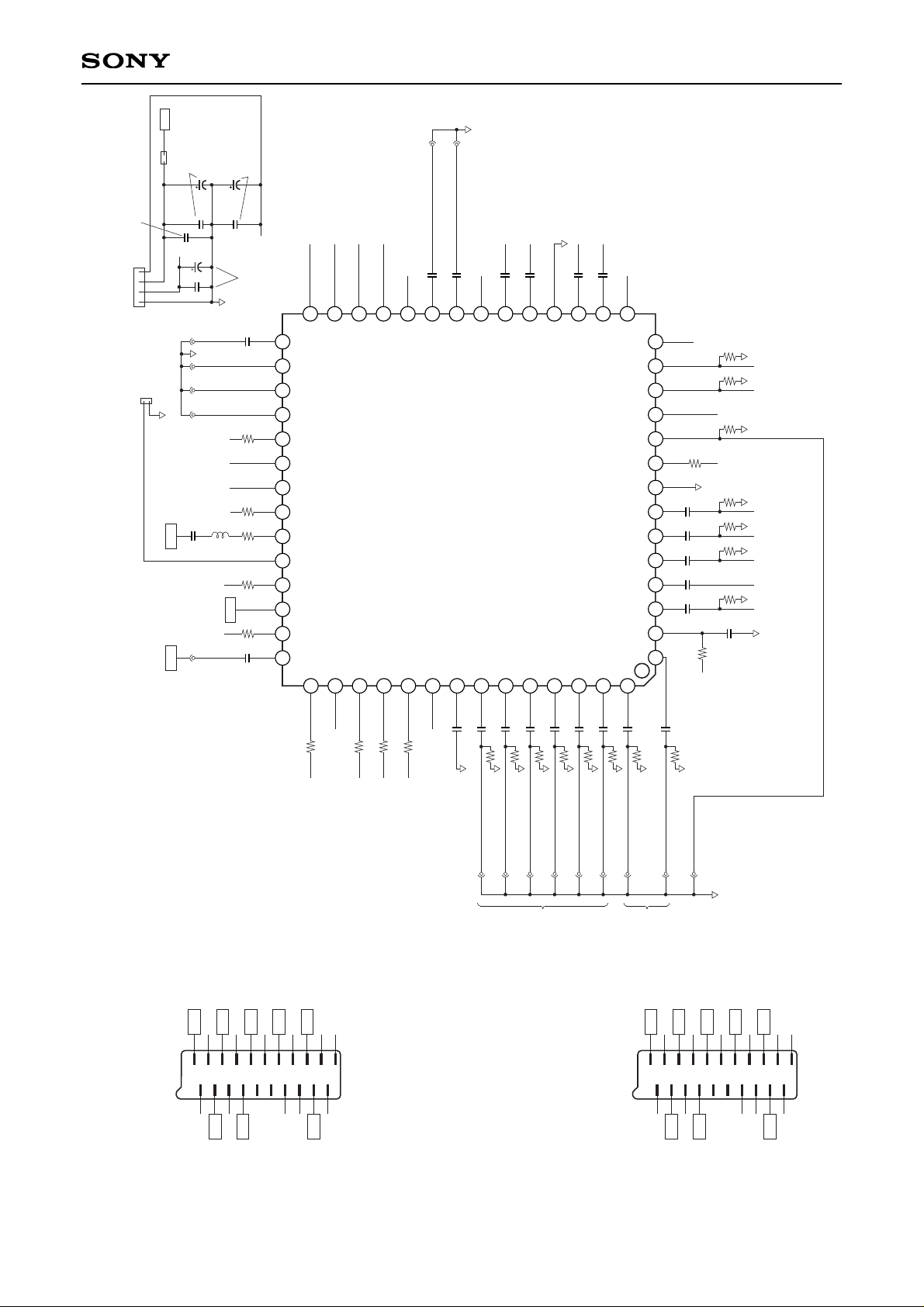
Application Circuit 2
Dual Supply
+12V
+5V
TV_FNC
TV_FBLANK
10kΩ
VCR_FNC
–5V
+5V
TV_LOUT
VCR_RIN
VCR_LIN
TV_RIN
TV_LIN
TV_ROUT
VCR_LOUT
VCR_ROUT
100nF
100nF
100nF
100nF
100nF
100nF
DIGITAL_AUDIO_R
Digital Audio Input
DIGITAL_AUDIO_L
75Ω
VCR_FBLANK
75Ω
VCR_BLUE
75Ω
75Ω75Ω
VCR_GREEN
100nF
75Ω
VCR_RED/C
100nF
VCR_CVBS_IN
100nF
75Ω
68kΩ
TV_CVBS_IN
100nF100nF
100nF
+5V
75Ω
100nF
75Ω
100nF
100nF
DIG_GREEN
DIG_BLUE
75Ω
100nF
DIG_RED
75Ω
100nF
DIG_CHROMA
75Ω
100nF
DIG_CVBS
75Ω
100nF
DIG_LUMA
75Ω
100nF
AUX_Y/CVBS
75Ω
100nF
AUX_C
DIG_FBLANK
VOUT_7 to RF Modulator
GNDGND
GND
TV_CVBS_OUT
VCR_RED/C
VCR_CVBS_OUT
+5V
SCL
SDA
+5V
75Ω
75Ω100nF 75Ω
1.8kΩ
12pF
10kΩ
10kΩ
100nF
TV_RED/C
75Ω
TV_GREEN
75Ω
TV_BLUE
+5V
+5V
75Ω
AUX_L
100µH
10µF
10µF
100nF
100nF
100nF
100nF
10µF
Supplies
Place close to Pin 44
–5V
VCC
+5V
TV
21
19
TV_CVBS_OUT
17
15
TV_RED/C
13
11
TV_GREEN
9
7
TV_BLUE
5
3
TV_LOUT1TV_ROUT
20
TV_CVBS_IN
18
16
TV_FBLANK
141210
8
TV_FNC
6
TV_LIN
4
2
TV_RIN
GND
GND
GND
GND
GND
GND
GND
GND
VCR
21
19
VCR_CVBS_OUT
17
15
VCR_RED/C
13
11
VCR_GREEN
9
7
VCR_BLUE
5
3
VCR_LOUT1VCR_ROUT
20
VCR_CVBS_IN
18
16
VCR_FBLANK
141210
8
VCR_FNC
6
VCR_LIN
4
2
VCR_RIN
GND
GND
GND
GND
GND
GND
GND
GND
Digital encoder
inputs
AUX video
inputs
Digital fast
blank
AUX_R
1 2 3 4 5 6 7 8 9 11 12 13 14
15
16
17
18
19
21
22
23
24
25
26
27
28
293132333435363738394142
43
44
45
46
47
48
49
50
51
52
53
54
55
56
10
20
3040
+12V
+5V_VOUT
VOUT_3
VOUT_2
VOUT_1
+5V_VID
VID_BIAS
VIN_1
VIN_3
VIN_5
VIN_6
VIN_8
VIN_9
SYNC_ID
VIN_11
VIN_10
VIN_7
VlN_4
VIN_2
GND_DIG
TV_FBLK
FBLK_IN1
FNC_TV
FBLK_IN2
FNC VCR
VOUT_5
GND_VID
VOUT_6
VOUT_7
TRAP
INTRUPT
SCL
SDA
LOGIC
MONO
PHONO_R
PHONO_L
LOUT1
RTV
LTV
+5V/12V_VCCA
RIN_1
LIN_1
–5V_GNDA
RIN_2
LIN_2
AUD_BIAS
RIN_3
LIN_3
+5V_
DIG
+12V_
DIG
LlN_4
RIN_4
VIN_13
VIN_12
VOUT_4
ROUT1
CXA2161R
Place close to Pin 21
Place close
to Pin 24
Place close to Pin 14
Application circuits shown are typical
examples illustrating the operation of
the devices. Sony cannot assume
responsibility for any problems arising
out of the use of these circuits or for
any infringement of third party patent
and other right due to same.
Page 41

– 41 –
CXA2161R
Notes on operation
1) Supply de-coupling capacitors, 10nF and 10µF in parallel should be inserted as close as possible to the
supply Pins 14, 15, 24 and 44. When using the dual supply configuration apply the capacitors to Pin 21 in
addition to the listed supply pins.
2) For best results with dual supply configuration, two +5V supplies should be used, audio (Pin 24) and
video/digital (Pins 14, 44 and 49).
3) To minimize crosstalk, attention should be given to the routing of audio and video to the IC inputs. PCB track
lengths should be kept as short as possible and preferably, audio placed on a separate layer to the video.
4) Attention should be given to the electrolytic capacitors on the output pins. In single supply configuration the
audio pin dc bias voltage will be approximately 6.0V, therefore the positive terminal of the capacitors should
be orientated towards the device pin.
5) To minimise stray capacitance the 75Ω series resistor on video outputs VOUT_1 to VOUT_6 should be
mounted as close as possible to the device Pins 47, 46, 45, 44, 41 and 39.
6) When driving video loads with impedance of 75Ω, video output VOUT_7 (Pin 38) must be connected to the
load via a buffer or line driver. This buffer should be located close to the output (Pin 38).
7) In dual supply mode, series protection resistors may be added on Audio outputs which are connected Scart
connectors.
Page 42
– 42 –
CXA2161R
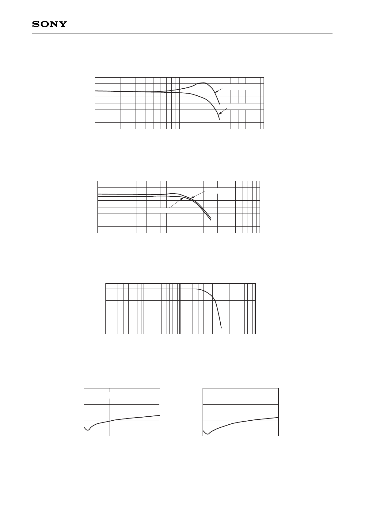
Typical Performance Curves
8
7
6
5
1
Gain [dB]
Frequency [MHz]
Video gain – VOUT_1, 2, 3, 4, 5, 6
10 100
4
3
2
1
0
VOUT_1, 2, 3
VOUT_4, 5, 6
8
7
6
5
1
Gain [dB]
Frequency [MHz]
Video gain – VOUT_7
10 100
4
3
2
1
0
Mixer Off
Mixer On
0.00
–1.00
1
Gain [dB]
Frequency [kHz]
Audio gain
10010 100001000
–2.00
–3.00
–4.00
1
0.1
0.00 1.00 2.00 3.00
THD [%]
Input level [Vrms]
Audio output distortion
TV outputs
0.01
0.001
Single supply configuration
1
0.1
0.00 1.00 2.00 3.00
THD [%]
Input level [Vrms]
Audio output distortion
ROUT1, LOUT1
0.01
0.001
Single supply configuration
Page 43

– 43 –
CXA2161R
Package Outline Unit: mm
SONY CODE
EIAJ CODE
JEDEC CODE
PACKAGE MATERIAL
LEAD TREATMENT
LEAD MATERIAL
PACKAGE MASS
EPOXY RESIN
PALLADIUM PLATING
COPPER ALLOY
PACKAGE STRUCTURE
56PIN LQFP(PLASTIC)
DETAIL
A
NOTE: Dimension “∗” does not include mold protrusion.
(0.3)
0.32 – 0.07
+ 0.08
(0.125)
0.145 – 0.025
+ 0.04
0° to 10°
(0.5)
(11.0)
0.6 ± 0.15
0.25
0.1 ± 0.1
DETAIL
B
0.1
0.13
M
∗ 10.0 ± 0.1
12.0 ± 0.2
0.65
A
B
1.7MAX
0.32 – 0.07
+ 0.08
1
56
14
15
28
29
42
43
LQFP-56P-L01
LQFP056-P-1010
0.3g
Sony Corporation
 Loading...