

Page 1
—1—
E99946A9Y-TE
Sony reserves the right to change products and specifications without prior notice. This information does not convey any license by
any implication or otherwise under any patents or other right. Application circuits shown, if any, are typical examples illustrating the
operation of the devices. Sony cannot assume responsibility for any problems arising out of the use of these circuits.
Absolute Maximum Ratings
(Ta=25 °C unless stated)
• Supply voltage VCC 12 V
• Storage temperature Tstg –65 to +150 °C
• Allowable power dissipation
PD 900 mW
Operating Conditions
• Supply voltage VCC 9+/–0.5 V
• Typical supply current 75 mA
• Operating temperature Topr –20 to +75 °C
Description
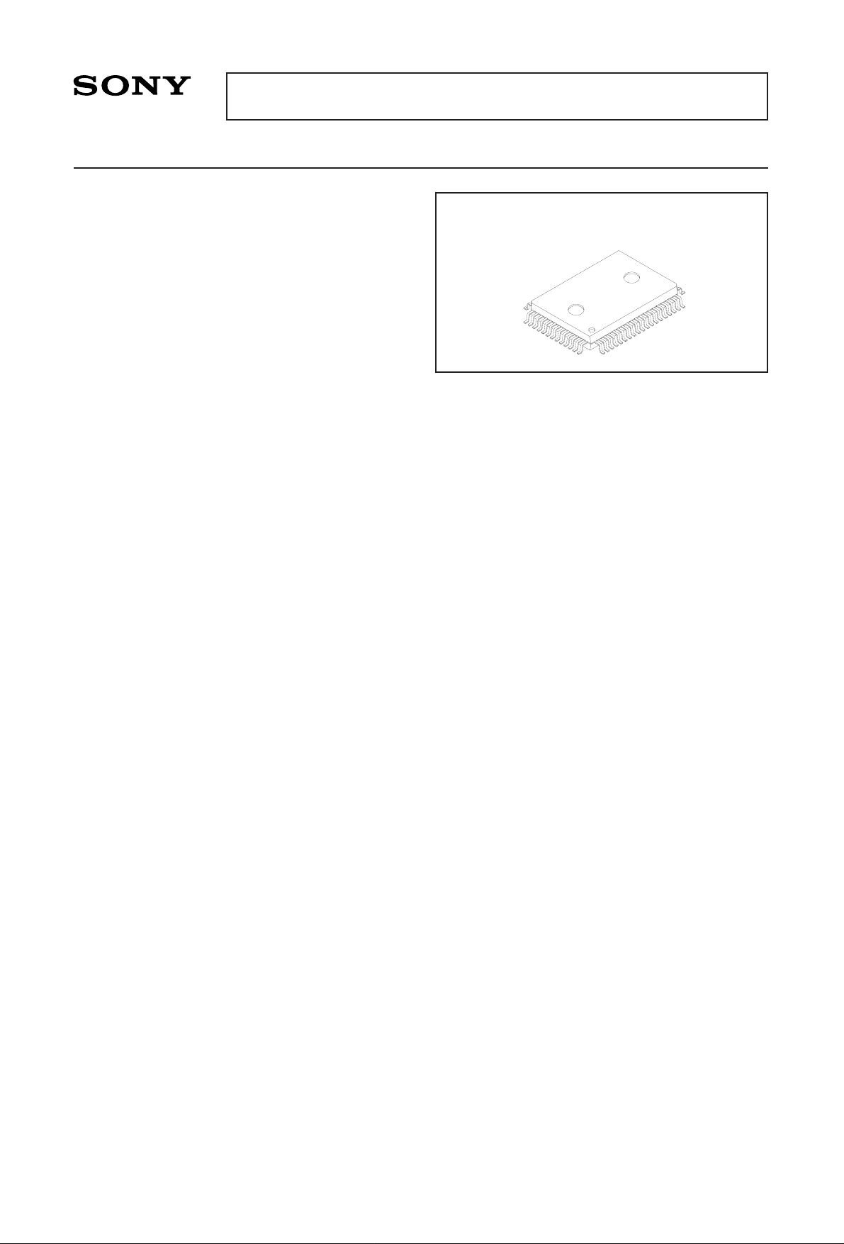
The CXA2149Q is a video and audio switch IC
featuring I2C bus compatibility for TV’s. The IC has
input pins that are compatible with the SCART
protocols. It offers other features such as an
electronic mute function with switching noise
reduction (zero cross detection), electronic volume
control, automatic SYNC pulse detection, and group
delay control.
Features
• 3 CVBS inputs.
• 2 CVBS outputs.
• Group delay control on TV and CVIN1.
• SYNC ID on TV and CVIN1.
• 3 Y/C inputs.
• 2 Y/C outputs.
• 6 L/R/2 inputs.
• 3 L/R/2 outputs.
• Mode inputs compatible with the SCART protocol.
• 3 Y/C mixer circuits.
• Audio muting via software control.
• External muting input.
• Audio switching noise elimination circuit.
• Volume adjustment via software control on L/R
channel 3.
• Wide band video amplifiers (20 MHz, –3 dB).
• Wide audio dynamic range (3 Vrms typ)
• Serial control via I2C bus.
• Separate control of video and audio switches.
• High impedance maintained by I2C lines (SDA,
SCL) even when power is off.
• Configurable dual slave address 90/92.
• I2C bus 5 and 3.3 V compatible.
Applications
TV’s
Structure
Bipolar silicon monolithic IC
I2C-Bus-Compatible Audio/Video Switch
64 pin QFP (Plastic)
CXA2149Q
For the availability of this product, please contact the sales office.
Page 2
—2—
CXA2149Q
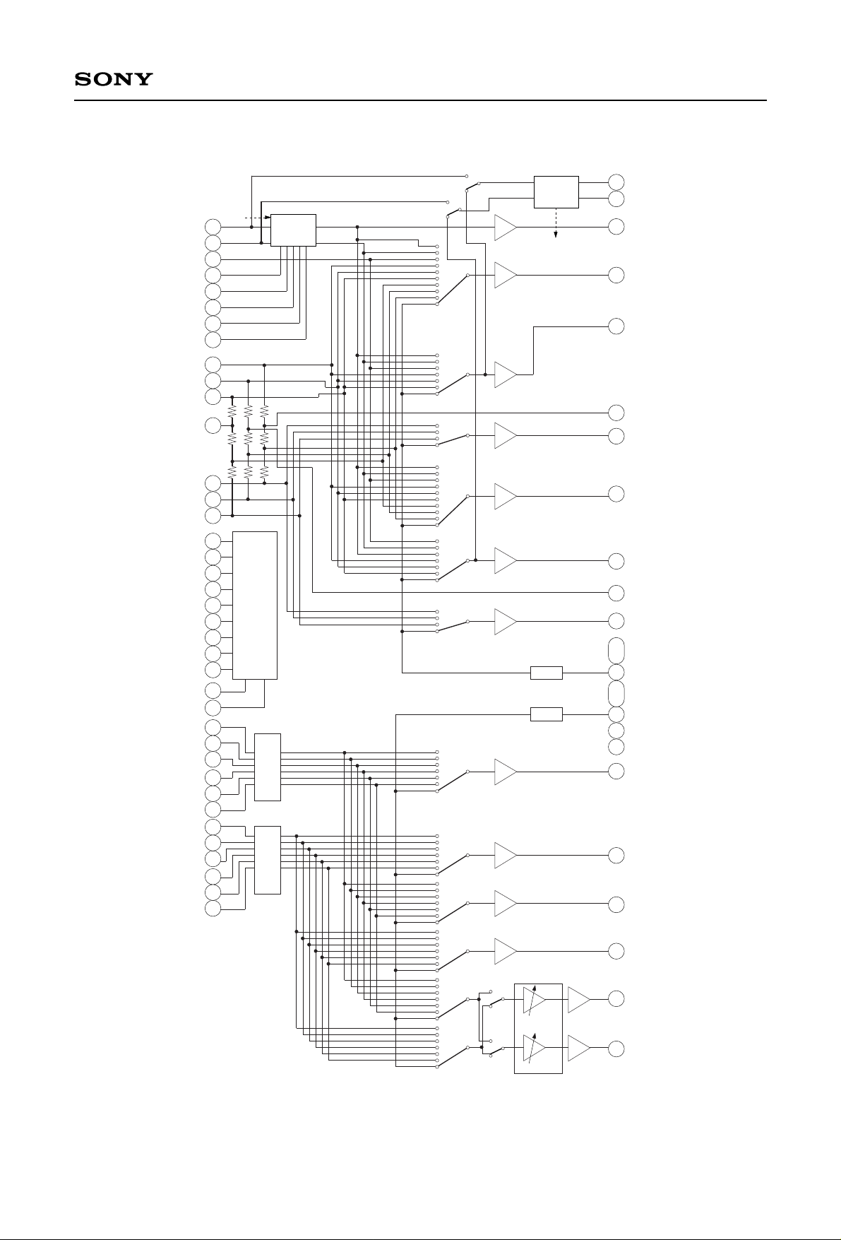
Block Diagram
REXT
TVOUT
RGD4
RGD3
LO0
RGD2
RGD1
LO1
CVOUT1
TRAP1
YOUT1
COUT1
SCL
SDA
ADR
MUTE
MODE1
MODE2
C2
C3
COUT2
TRAP2
YOUT2
DVCC
CVOUT2
DGND
LOUT2
ROUT2
LOUT1
ROUT1
RV1
RV2
RV3
RV4
RV5
RTV
AGND
LV1
LV2
LV3
LV4
LV5
LTV
ROUT3
LOUT3
ABIAS
AVCC
MODE3
C1
Y3
TRAP3
VBIAS
Y2
VGND1, 2
Y1
VVCC1, 2
CVIN2
TC2
CVIN1
TC1
TV
SYNC
DETECT
GROUP
DELAYS
I C
6dB
6dB
0dB
0dB
6dB
0dB
0dB
6dB
6dB
6dB
6dB
6dB
6dB
I C
LOGIC
BIAS
BIAS
–6dB
–6dB
0 to –63dB
0 to –63dB
38
39
40
41
21
23
24
2
9
11
10
13
45
47
46
43
59
12
55
57
22
31
61
63
1
3
4
6
7
60
62
64
54
53
56
58
49
51
52
14
15
16
17
18
19
42
44
20
5
8
25
26
27
28
29
30
33
34
35
36
37
32
2
I C
2
2
,
48
,
Page 3
—3—
CXA2149Q
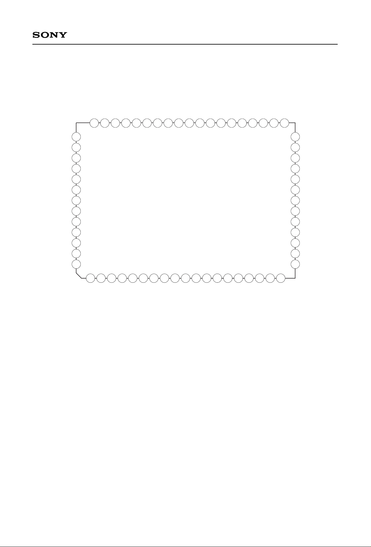
Pin Configuration
1 2 3 4 5 6 7 8 9
10 11 12
13
14 15 16 17 18 19
33343536373839404142434445464748495051
REXT
TVOUT
RGD4
RGD3
LO0
RGD2
RGD1
LO1
CVOUT1
TRAP1
YOUT1
VVCC2
COUT1
SCL
SDA
ADR
MUTE
MODE1
MODE2
C2
NC
C3
VGND2
COUT2
TRAP2
YOUT2
DVCC
CVOUT2
DGND
LOUT2
ROUT2
LOUT1
ROUT1
RV1
RV2
RV3
RV4
RV5
52
53
54
55
56
57
58
59
60
61
62
63
64 20
21
22
23
24
25
26
27
28
29
30
31
32
RTV
AGND
LV1
LV2
LV3
LV4
LV5
LTV
ROUT3
LOUT3
ABIAS
AVCC
MODE3
C1
TRAP3
Y3
VBIAS
Y2
VGND1
Y1
VVCC1
CVIN2
TC2
CVIN1
TC1
TV
CXA2149Q
Page 4
—4—
CXA2149Q
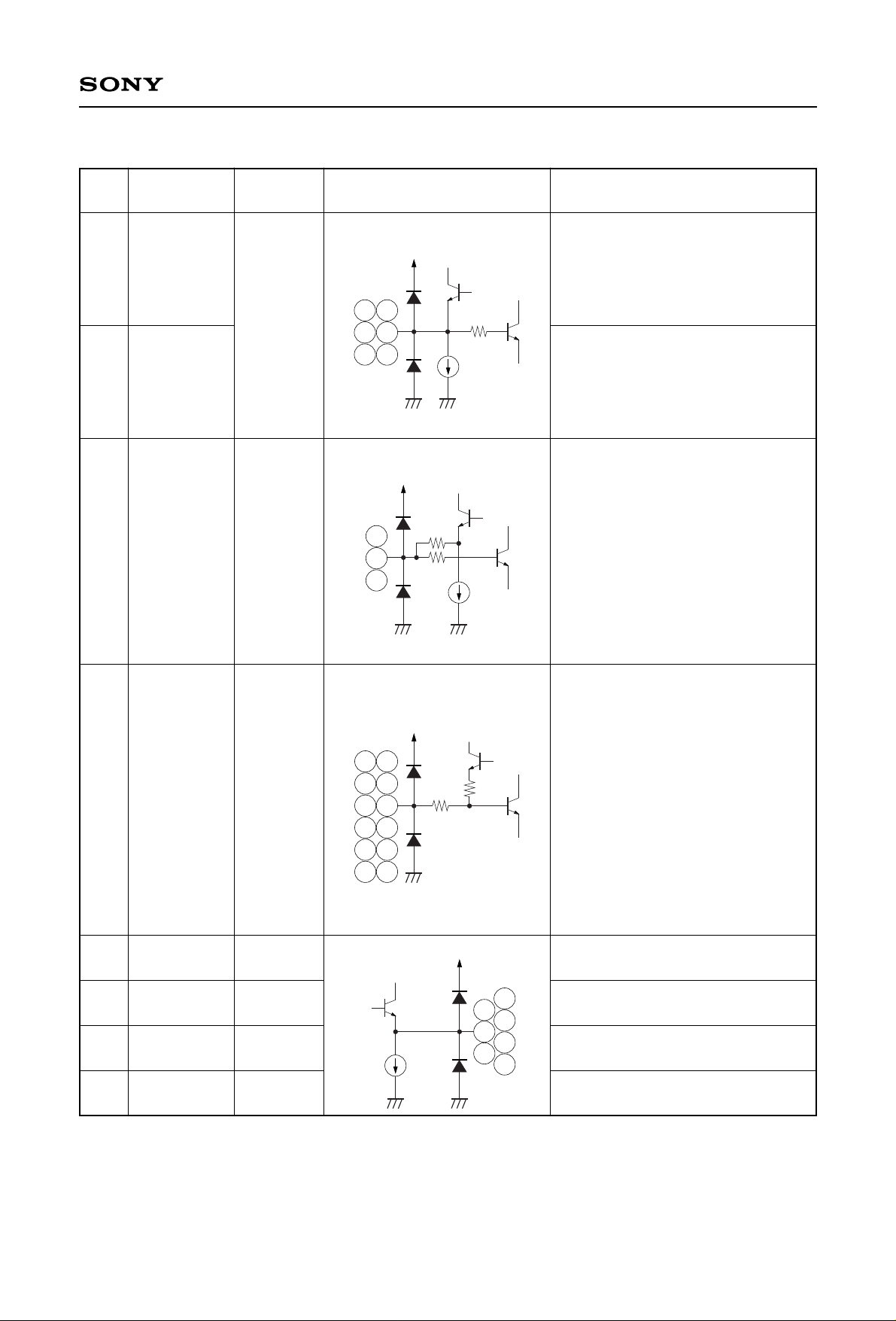
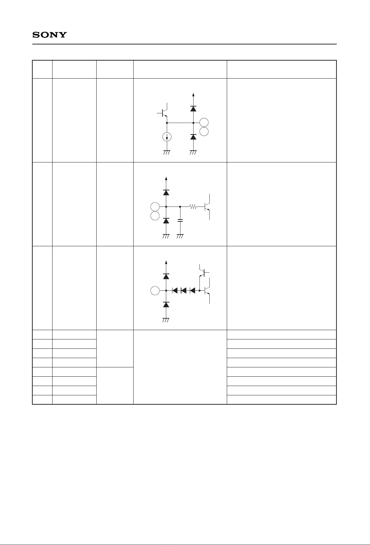
Pin Description
64
62
60
58
56
54
52
51
49
25
30
29
28
27
26
32
37
36
35
34
33
9
43
11
45
13
47
2
TV
CVIN1
CVIN2
Y1
Y2
Y3
C1
C2
C3
LTV
LV1
LV2
LV3
LV4
LV5
RTV
RV1
RV2
RV3
RV4
RV5
CVOUT1
CVOUT2
YOUT1
YOUT2
COUT1
COUT2
TVOUT
3.9
4.5
4.5
3.8
3.5
4.5
3.8
Pin
Symbol
Pin
Equivalent circuit Description
No voltage (V)
54
56
58
60
62
64
VCC
0.5µ
147
VCC
100µ
147
20k
49
51
52
5.2V
VCC
33k
33k
4.5V
25
26
27
28
29
30
32
33
34
35
36
37
VCC
1.8m
2
9
11
13
43
45
47
Video signal inputs.
Luminance signal inputs.
Chrominance signal inputs.
Audio signal inputs.
Composite video signal outputs.
Luminance signal outputs.
Chrominance signal outputs.
TV signal group delayed output.
Page 5
—5—
CXA2149Q
7
3
6
4
1
44
59
12
21
42
57
48
31
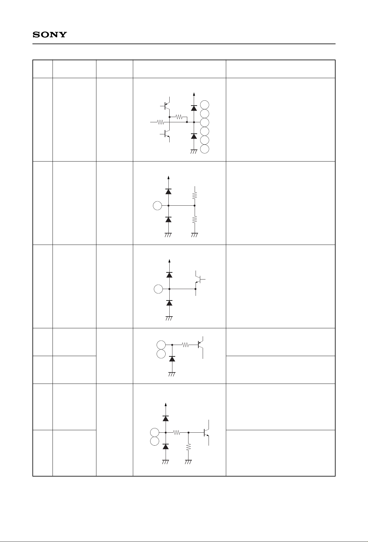
RGD1
RGD4
RGD2
RGD3
REXT
DVCC
VVCC1
VVCC2
AVCC
DGND
VGND1
VGND2
AGND
4.5
4.5
1.7
9
0
Pin
Symbol
Pin
Equivalent circuit Description
No voltage (V)
VCC
0.5m
3
7
VCC
1.7k
4
6
VCC
3.8V
1
Group delay output to external
filter.
Group delay inputs from external
filter.
Pin connection for 39 kΩ group delay
setting resistor. Pin voltage is group
delay control dependent.
Digital supply.
Video supply.
Video supply.
Audio supply.
Digital ground.
Video ground.
Video ground.
Audio ground.
Page 6
—6—
CXA2149Q
39
41
23
38
40
24
22
55
14
15
16
17
LOUT1
LOUT2
LOUT3
ROUT1
ROUT2
ROUT3
ABIAS
VBIAS
SCL
SDA
ADR
MUTE
4.5
4.5
4.5
Pin
Symbol
Pin
Equivalent circuit Description
No voltage (V)
VCC
4.5V
22
20k
20k
VCC
4.5V
55
14
15
4k
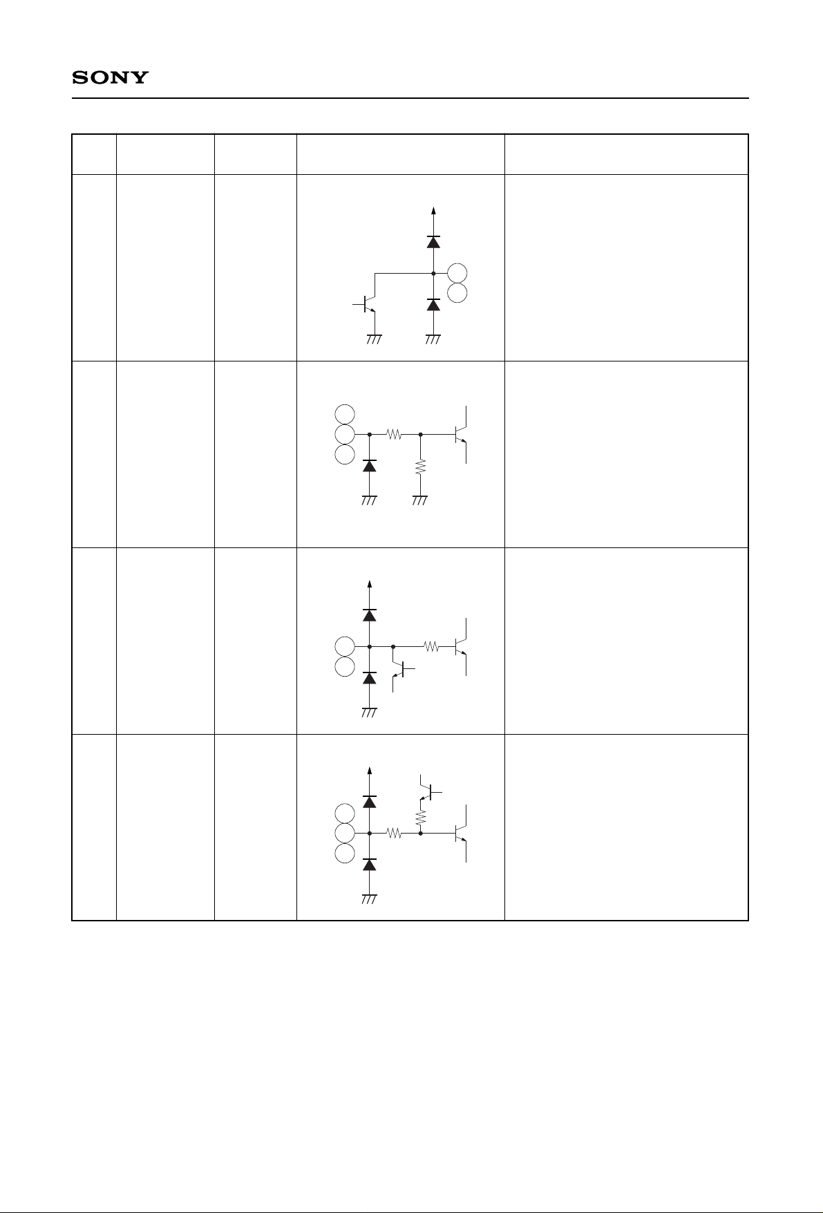
Audio signal outputs.
Internal reference bias for audio
circuits. A capacitor is connected
from this pin to GND.
Internal reference bias for video
circuits. A capacitor is connected
from this pin to GND.
I2C bus clock line.
I2C bus data line.
Slave address control.
Audio signal output mute.
VCC
72k
28k
16
17
VCC
23
24
38
39
40
41
56
20k
Page 7
—7—
CXA2149Q
5
8
18
19
20
63
61
10
46
53
LO0
LO1
MODE1
MODE2
MODE3
TC1
TC2
TRAP1
TRAP2
TRAP3
5
3.5
Pin
Symbol
Pin
Equivalent circuit Description
No voltage (V)
VCC
5
8
I C
control
2
25k
25k
19
18
20
VCC
147
61
63
VCC
200
200
46
10
53
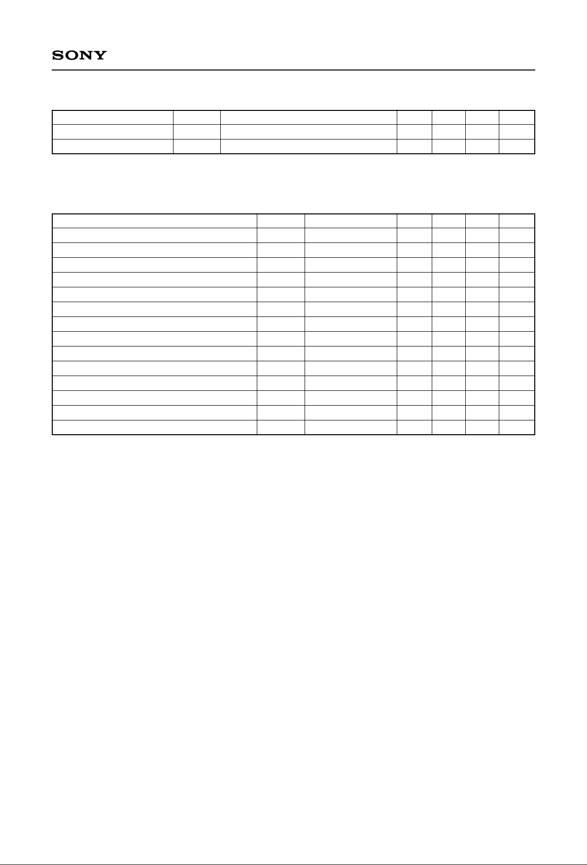
Open collector logic outputs.
Function SCART inputs from SCART
connectors.
Video detect time constant capacitor
connection pins.
Connects trap circuit for subcarrier.
Note. Pin voltages indicated the approximate DC voltage levels with no signals inputs.
Page 8
—8—
CXA2149Q
Electrical Characteristics (Ta=25 °C, VCC=9 V unless stated.)
Item
Supply voltage
Supply current
Symbol
VCC
ICC
Conditions Min. Typ. Max. Unit
8.5 9.0 9.5 V
40 75 100 mA
I2C (Operation of the I2C using either a 3.3 or 5 V supply on the external controller is possible)
Item
High level input voltage
Low level input voltage
Low level output voltage
Max. clock frequency
Min. waiting time for data change
Min. waiting time for data transfer start
Low level clock pulse width
High level clock pulse width
Min. waiting time for start preparation
Min. data hold time
Min data preparation time
Rise time
Fall time
Min. waiting time for stop preparation
Symbol
VIH
VIL
VOL
fSCL
tBUF
tHDSTA
tL
tH
tSUSTA
tHDDAT
tSUDAT
tR
tF
tSUSTO
Conditions
SDA 3 mA sink
Min. Typ. Max. Unit
2.3 — 5 V
0 — 1.5 V
0 — 0.4 V
0 — 100 kHz
4.5 — — µs
4 — — µs
4.7 — — µs
4 — — µs
4.7 — — µs
5 — — s
250 — — ns
— — 1 µs
— — 300 ns
4.7 50 — µs
Page 9
—9—
CXA2149Q
Audio System
Item
Gain
Channel 1/Channel 2
Channel 3 (max.)
Channel 3 (min.)
–3 dB bandwidth
Total harmonic distortion
Input dynamic range
Crosstalk
Ripple rejection ratio
Output DC offset
Input impedance
Output impedance
Phase difference
S/N ratio
Mute
Volume control
Fine
Coarse
Symbol
FGVA1
VGVAF
VGVA0
FBWA
THD
VDRA
VCtA
RRA
Voff
Zin
Zout
VPDA
S/NA
Amute
FEVC
CEVC
Conditions
f=1 kHz, 1 Vp-p I/P.
1 Vp-p I/P, 1 kHz serving as 0 dB ref.
f=1 kHz, 0.5 Vp-p I/P with a 400 Hz to
80 kHz passband.
f=100 kHz, distortion at O/P less than
0.3 %
f=1 kHz, 1 Vp-p I/P, measure other
outputs.
f=100 Hz, 0.3 Vp-p signal applied to
AVCC
Offset voltage between I/P and O/P.
f=1 kHz, 1 Vrms input.
Compare left and right channels.
f=1 kHz, 1 Vp-p input with a 20 Hz to
20 kHz passband. See note 1.
f=1 kHz, 1 Vp-p input.
f=1 kHz, 0.5 Vp-p input.
Min. Typ. Max. Unit
–0.5 0 0.5 dB
–0.5 0 0.5 dB
–68 –63 –58 dB
— 1 — MHz
— 0.01 0.05 %
2.8 3.0 — Vrms
— –90 –76 dB
— –55 — dB
–30 0 30 mV
— 66 — kΩ
— 20 — Ω
— 0.1 — Deg
85 90 — dB
— –90 –70 dB
0.6 1 1.4 dB
7.6 8 8.4 dB
Audio System Notes
1. Channel 3 should be set at maximum volume.
Page 10

—10—
CXA2149Q
Video System
Item
CVOUT1/2 gain
Y/COUT1/2 gain
–3 dB bandwidth
–3 dB bandwidth
Y/C mixer
Input level, TV and CVIN1
Input dynamic range,
CVIN2 and Y inputs.
Crosstalk
S/N ratio
Differential gain
Differential phase
Group delay
SYNC identification
detected when
SYNC amplitude
SYNC duty cycle
not detected when
SYNC amplitude
SYNC duty cycle
Symbol
GVCV
GVYC
FBWV1
FBWV2
VRIV
VDRV
VCtV
S/NV
DG
DP
GD
SYNC1
Conditions
f=200 kHz, 0.3 Vp-p I/P.
f=200 kHz, 0.3 Vp-p I/P.
0.3 Vp-p I/P. See note 1.
0.3 Vp-p I/P. See note 1.
f=200 kHz, distortion at O/P less
than 1 %, GD=OFF
f=200 kHz, distortion at O/P less
than 1.0 %.
f=4.43 MHz, 0.7 Vp-p I/P,
measure other outputs.
Ratio of 0.7 Vp-p white level to
‘black line’ noise. 5 kHz to 5 MHz
passband. See note 2.
1.4 Vp-p 5 step staircase,
modulated with 150 mVp-p 4.43 MHz.
As above.
f=200 kHz, 0.7 Vp-p.
See figure 1 and note 3.
See note 4.
64 µs period.
64 µs period.
Min. Typ. Max. Unit
5.5 6 6.5 dB
–0.5 0 0.5 dB
15 20 — MHz
10 15 — MHz
1.4 — — Vp-p
1.7 — — Vp-p
— –55 — dB
— 72 — dB
–1.5 0 1.5 %
–1.5 0 1.5 Deg
200 250 350 ns
100 — — mV
91 — — %
— — 30 mV
— — 84 %
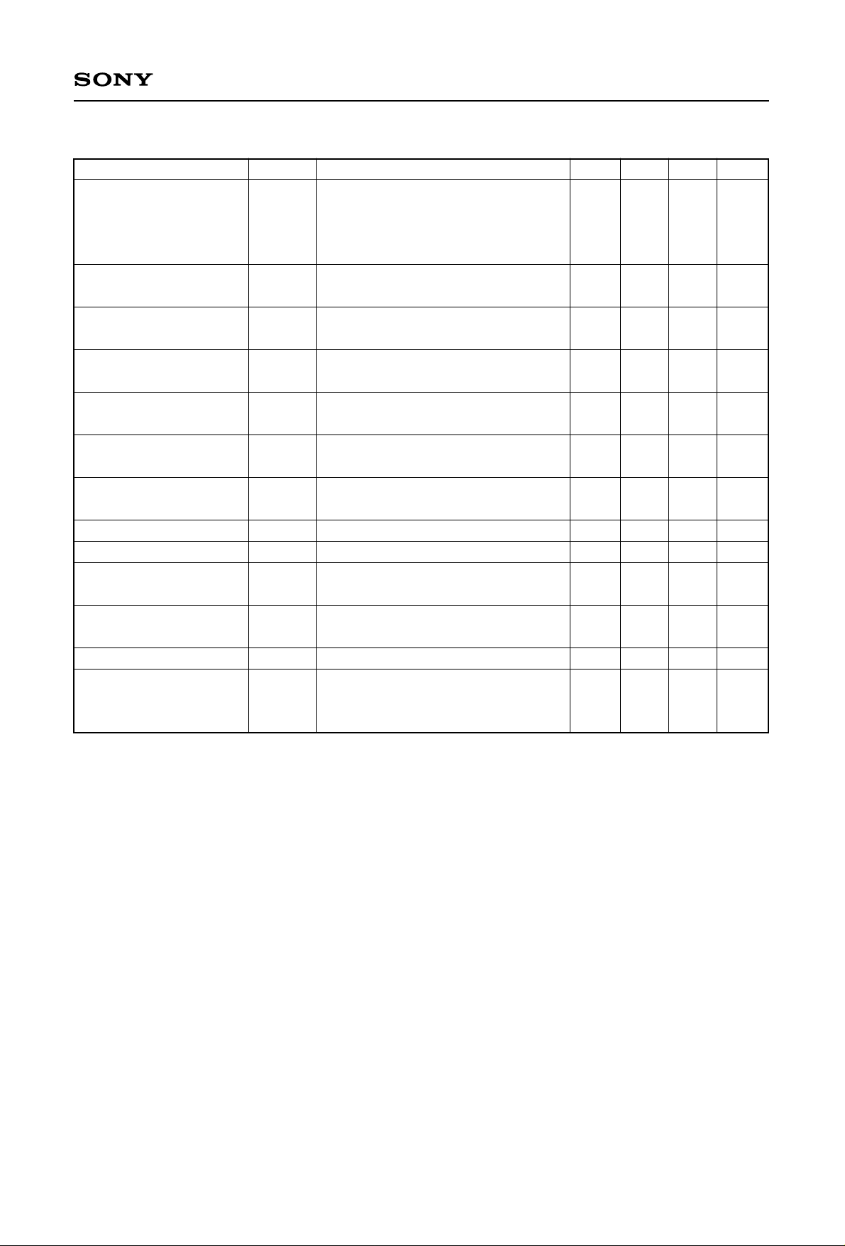
Figure 1 Group delay characteristic
Frequency (Hz)
4.5
4
3.5
3
2.5
2
1.5
1
0 1 2 3 4 5 6
Group delay (seconds)
×10
–7
×10
6
Page 11

—11—
CXA2149Q
Video System Notes
1. 200 kHz is taken to be 0 dB for the purpose of this measurement. Where applicable, the group delay
function will be turned off to make this measurement.
2. Weighted using CCIR567.
3. This group delay characteristic, figure 1, is for the B, G specifications. It does not take into account the
input and output delays inherent within the AV switch.
4. The sync detection circuits operate on the video sources that have been switched into the TV and CVIN1
channels, respectively.
The internal SYNC discriminator circuit functions in the following way. The SYNC tip of the incoming video
input is clamped to a fixed level and the signal is then compared in magnitude with an internal threshold
voltage. If the signal is smaller than the threshold level the IC determines that the SYNC does not exist.
Conversely, if the signal is found to be greater than the threshold then the duty cycle of signal is passed to
the duty discrimination circuit. The discriminator circuit will identify whether the duty cycle of the signal is
above 91 % at which point SYNC is detected, or below 84 % when SYNC is not detected.
To prevent occasional video disturbances such as IF noise from the tuner causing malfunctioning of the
SYNC detector, a time constant of approximately 14 line periods is applied during which the status of the
SYNC detection is maintained.
Page 12

—12—
CXA2149Q
Video System Test Configuration (gain, dynamic range, bandwidth, signal to noise, crosstalk, differential gain, differential phase, sync ID, group delay)
Signals applied to inputs on Pins 64, 62, 60, 58, 56, 54, 52, 51, 49
Output signal measured form Pins 9, 11, 13, 43, 45, 47
Notes:
1) All +9 V supplies de-coupled close to supply Pins 21, 44, 59 with 10 nF ceramic capacitor.
2) Refer to application schematic for external pin configuration of sync detect circuits.
3) Input signal assumes 75 ohm video driver. All video outputs are loaded with an emitter follower during tests.
REXT
TVOUT
RGD4
RGD3
LO0
RGD2
RGD1
LO1
CVOUT1
TRAP1
YOUT1
VVCC2
COUT1
SCL
SDA
ADR
MUTE
MODE1
MODE2
C2
NC
C3
VGND2
COUT2
TRAP2
YOUT2
DVCC
CVOUT2
DGND
LOUT2
ROUT2
LOUT1
ROUT1
RV1
RV2
RV3
RV4
RV5
RTV
AGND
LV1
LV2
LV3
LV4
LV5
LTV
ROUT3
LOUT3
ABIAS
AVCC
MODE3
C1
TRAP3
Y3
VBIAS
Y2
VGND1
Y1
VVCC1
CVIN2
TC2
CVIN1
TC1
TV
CXA2149Q
100nF
100nF
100nF
75
75
75
+9V
+12V
1k
BC547B
+12V
1k
BC547B
+12V
+12V
1k
BC547B
BC547B
1k
100nF
100nF
75
100nF
75
100nF
75
1µF
75
100nF
75
+9V
+9V
1µF
75
Input Signal
10µF 100nF
V
Measurement Point
+12V
BC547B
1k
+12V
BC547B
1k
+12V
BC547B
1k
200
200
52
53
54
55
56
57
58
59
60
61
62
63
64
33343536373839404142434445464748495051
20
21
22
23
24
25
26
27
28
29
30
31
32
10µF
I C
2
39k
3.3k
3.3k 3.3k
1 2
3 4
5
6 7
8 9
10 11 12
13
14 15 16 17 18 19
Video Test Configuration
Page 13

—13—
CXA2149Q
Audio System Test Configuration (gain, dynamic range, signal to noise, crosstalk, distortion, volume control, ZCD and mute)
Signals applied to inputs on Pins 25, 26, 27, 28, 29, 30, 32, 33, 34, 35, 36, 37
Output signal measured form Pins 23, 24, 39, 40, 41
Notes:
1) All +9 V supplies de-coupled close to supply Pins 21, 44, 59 with 10 nF ceramic capacitor.
2) When muting audio using hardware mute, SW1 is closed.
REXT
TVOUT
RGD4
RGD3
LO0
RGD2
RGD1
LO1
CVOUT1
TRAP1
YOUT1
VVCC2
COUT1
SCL
SDA
ADR
MUTE
MODE1
MODE2
C2
NC
C3
VGND2
COUT2
TRAP2
YOUT2
DVCC
CVOUT2
DGND
LOUT2
ROUT2
LOUT1
ROUT1
RV1
RV2
RV3
RV4
RV5
RTV
AGND
LV1
LV2
LV3
LV4
LV5
LTV
ROUT3
LOUT3
ABIAS
AVCC
MODE3
C1
TRAP3
Y3
VBIAS
Y2
VGND1
Y1
VVCC1
CVIN2
TC2
CVIN1
TC1
TV
CXA2149Q
1µF
1k
+9V
100nF
+9V
+9V
+5V
10µF 100nF
200
200
1 2 3 4 5 6 7 8 9
10 11 12
13
14 15
16
17 18 19
10µF
1µF
1k
1µF
1k
1µF
1k
1µF
1k
10µF
10µF10µF
10µF
33343536373839404142434445464748495051
V
10k
Measurement
Point
SW1
HW mute
10µF
1µF
10µF
1k
1µF1k1µF1k1µF1k1µF1k1µF
1k
1µF
1k
Input Signal
20
21
22
23
24
25
26
27
28
29
30
31
32
52
53
54
55
56
57
58
59
60
61
62
63
64
I C
2
Audio Test Configuration
Page 14

—14—
CXA2149Q
DC Tests (Audio and Video System)
Notes:
1) All +9 V supplies de-coupled close to supply Pins 21, 44, 59 with 10 nF ceramic capacitor.
2) All video outputs are loaded with an emitter follower during test.
REXT
TVOUT
RGD4
RGD3
LO0
RGD2
RGD1
LO1
CVOUT1
TRAP1
YOUT1
VVCC2
COUT1
SCL
SDA
ADR
MUTE
MODE1
MODE2
C2
NC
C3
VGND2
COUT2
TRAP2
YOUT2
DVCC
CVOUT2
DGND
LOUT2
ROUT2
LOUT1
ROUT1
RV1
RV2
RV3
RV4
RV5
RTV
AGND
LV1
LV2
LV3
LV4
LV5
LTV
ROUT3
LOUT3
ABIAS
AVCC
MODE3
C1
TRAP3
Y3
VBIAS
Y2
VGND1
Y1
VVCC1
CVIN2
TC2
CVIN1
TC1
TV
CXA2149Q
+9V
100nF
+9V
+9V
10µF 100nF
200
200
10µF
V
Video Output
Signal
Measurement
Audio Input
Signal
Measurement
I C
2
V
Video Input
Signal
Measurement
V
Audio Output
Signal
Measurement
V
1 2
3 4
5
6 7
8 9
10 11 12
13
14 15 16 17 18 19
52
53
54
55
56
57
58
59
60
61
62
63
64 20
21
22
23
24
25
26
27
28
29
30
31
32
33343536373839404142434445464748495051
DC Test Configuration
Page 15
—15—
CXA2149Q
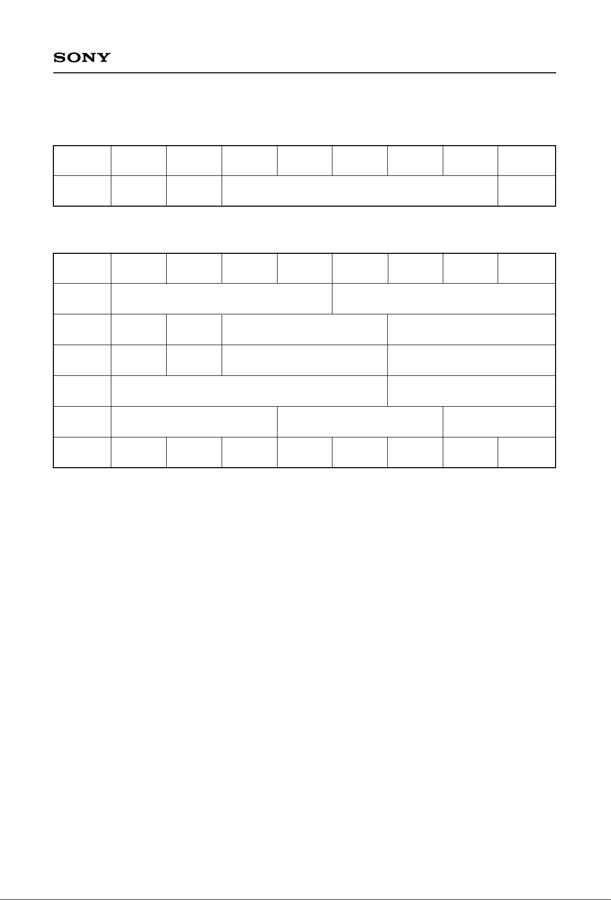
I2C Bus Register Assignment
Status Register
Slave
1 0 0 1 0 0 ADR R/W
Address
Data1
SYNC1 SYNC2 Mode
POR
Status status Status
Slave
1 0 0 1 0 0 ADR R/W
Address
Data1 CVOUT1 CVOUT2
Data2
LO0 LO1
YCOUT1 YCOUT2
Control Control
Data3
ZCD AOUT3
AOUT1 AOUT2
Switch Mute
Data4
Group
AOUT3
Delay
Data5
AOUT3 Volume Control AOUT3 Volume Control AOUT3L/R
Coarse Fine Switch
Data6
GD1 GD2 SYNC1 SYNC2
∗ ∗ ∗ ∗
Switch Switch Switch Switch
Control Registers
Note.
1. The names CVOUT1, YCOUT1, AOUT1 etc., refer to the particular output or outputs that the register
controls.
2. ∗ Register undefined.
Status Register Descriptions
SYNC Detection Circuits Data1 Bit 6 (SYNC1) and Bit 7 (SYNC2)
Indicates whether a video signal is present or not. SYNC1 takes its input from TV and YOUT1. SYNC2 takes
its input from CVIN1 and YOUT2.
SYNC1 or SYNC2 bit Meaning
0 no SYNC
1 SYNC present
Page 16

—16—
CXA2149Q
Mode Status Data1 Bits 1 to 5
The mode inputs from the SCART ports are driven at three different voltage levels to indicate the mode format
of the port. These inputs are detected and then encoded to the status register in the following manner.
Input pin voltage Meaning
0 to 2 V Internal TV
4.5 to 7 V External 16:9
9.5 to 12 V External 4:3
Mode status bits Meaning Meaning Meaning
for MODE1 for MODE2 for MODE3
00000 Internal TV Internal TV Internal TV
00001 External 16:9 Internal TV Internal TV
00010 External 4:3 Internal TV Internal TV
00011 Internal TV External 16:9 Internal TV
00100 External 16:9 External 16:9 Internal TV
00101 External 4:3 External 16:9 Internal TV
00110 Internal TV External 4:3 Internal TV
00111 External 16:9 External 4:3 Internal TV
01000 External 4:3 External 4:3 Internal TV
01001 Internal TV Internal TV External 16:9
01010 External 16:9 Internal TV External 16:9
01011 External 4:3 Internal TV External 16:9
01100 Internal TV External 16:9 External 16:9
01101 External 16:9 External 16:9 External 16:9
01110 External 4:3 External 16:9 External 16:9
01111 Internal TV External 4:3 External 16:9
10000 External 16:9 External 4:3 External 16:9
10001 External 4:3 External 4:3 External 16:9
10010 Internal TV Internal TV External 4:3
10011 External 16:9 Internal TV External 4:3
10100 External 4:3 Internal TV External 4:3
10101 Internal TV External 16:9 External 4:3
10110 External 16:9 External 16:9 External 4:3
10111 External 4:3 External 16:9 External 4:3
11000 Internal TV External 4:3 External 4:3
11001 External 16:9 External 4:3 External 4:3
11010 External 4:3 External 4:3 External 4:3
11011 to 11111 Not used Not used Not used
Page 17

—17—
CXA2149Q
Power on Reset Data1 Bit 0
After power on this bit will be set to 1 when DVCC, Pin 44, passes through a defined threshold level. The
control registers are then defined as below. After the first write command the bit will be reset to 0.
CVOUT1=CVOUT2=1001, LO0 switch=LO1 switch=1, YCOUT1=YCOUT2=111,
ZCD switch=AOUT3 mute=1, AOUT1=AOUT2=111, Group delay=10000,
AOUT3=111, AOUT3 volume control coarse=AOUT3 volume control fine=111,
AOUT3L/R switch=00, GD1 switch=GD2 switch=1, SYNC1 switch=SYNC2 switch=1.
Control Register Descriptions
Video Inputs
CVOUT1 Data1 Bits 4 to 7
These bits select the input signal that will be output on the CVOUT1 pin.
CVOUT1 Input or function selected
0000 TV
0001 CVin1
0010 CVin2
0011 Y1
0100 Y2
0101 Y3
0110 Y1+C1
0111 Y2+C2
1000 Y3+C3
1001 Mute
1010 to 1111 Not used
CVOUT2 Data1 Bits 0 to 3
These bits select the input signal that will be output on the CVOUT2 pin.
CVOUT2 Input or function selected
0000 TV
0001 CVin1
0010 CVin2
0011 Y1
0100 Y2
0101 Y3
0110 Y1+C1
0111 Y2+C2
1000 Y3+C3
1001 Mute
1010 to 111 Not used
Page 18

—18—
CXA2149Q
YCOUT1 Data2 Bits 3 to 5
These bits select the input signals that will be output on the YOUT1/COUT1 pins.
YCOUT1/2 Input or function selected
000 TV and Mute
001 CVin1 and Mute
010 CVin2 and Mute
011 Mute and Mute
100 Y1 and C1
101 Y2 and C2
110 Y3 and C3
111 Mute and Mute
YCOUT2 Data2 Bits 0 to 2
These bits select the input signals that will be output on the YOUT2/COUT2 pins.
YCOUT2 Input or function selected
000 TV and Mute
001 CVin1 and Mute
010 CVin2 and Mute
011 Mute and Mute
100 Y1 and C1
101 Y2 and C2
110 Y3 and C3
111 Mute and Mute
Page 19

—19—
CXA2149Q
Audio Inputs
AOUT1 Data3 Bits 3 to 5
These bits select the input signal that will be output on the ROUT1 and LOUT1.
AOUT1 bits Input or function selected
000 Mute
001 LTV and RTV
010 LV1 and RV1
011 LV2 and RV2
100 LV3 and RV3
101 LV4 and RV4
110 LV5 and RV5
111 Mute
AOUT2 Data3 Bits 0 to 2
These bits select the input signal that will be output on ROUT2 and LOUT2
AOUT2 bits Input or function selected
000 Mute
001 LTV and RTV
010 LV1 and RV1
011 LV2 and RV2
100 LV3 and RV3
101 LV4 and RV4
110 LV5 and RV5
111 Mute
AOUT3 Data4 Bits 0 to 2
These bits select the input signal that will be output on ROUT3 and LOUT3
AOUT3 bits Input or function selected
000 Mute
001 LTV and RTV
010 LV1 and RV1
011 LV2 and RV2
100 LV3 and RV3
101 LV4 and RV4
110 LV5 and RV5
111 Mute
Page 20

—20—
CXA2149Q
Group Delay Switches Data1 Bit 7 (GD1 Switch) and Bit 6 (GD2 Switch)
Switch the respective group delay function on or off. GD2 switches on and off the group delay on the TV input
and GD1 switches on and off the group delay on the CVIN1 input.
GD1 or GD2 bit Group delay function
0 off
1 on
Group Delay Control Data4 Bits 3 to 7
Used to control the variation in group delay. If no adjustment is required then set a value 10000.
Group Delay bits Change in the Max. delay frequency
00000 –800 kHz
11111 +800 kHz
AOUT3 Volume Control Coarse Data5 Bits 5 to 7
Selects the gain for the internal audio amplifiers in 8 dB steps.
Coarse bits Gain of AOUT3 channels
000 0 dB
111 –56 dB
AOUT3 Volume Control Fine Data5 Bits 2 to 4
Selects the gain for the internal audio amplifiers in 1 dB steps.
Fine bits Gain of AOUT3 channels
000 0 dB
111 –7 dB
AOUT3L/R Switch Data5 Bits 0 and 1
Controls which of channel 3’s left or right channels is output to LOUT3 and ROUT3, respectively.
AOUT3L/R bits Output to LOUT3 and ROUT3
00 Normal
01 Left channel
10 Right channel
11 Inverted
Page 21

—21—
CXA2149Q
AOUT3 Mute Switch Data3 Bit 6
Mutes the LOUT3 and ROUT3 channels at the electronic volume control output so that a click free audio
channel change can take place.
AOUT3 mute bit Meaning
0 Mute off
1 Mute on
The normal sequence for a click free channel change is as follows:-
1. Mute the channel 3 outputs (AOUT3 mute=1) with zero cross detection on (ZCD switch=1).
2. Change the channel 3 audio source, AOUT3L/R control.
3. Un-mute the channel 3 outputs still with zero cross detection on.
LO0 or LO1 Control Data2 Bit 7 (LO0 control) and Bit 6 (LO1 control)
Used to control the switching of the open collector outputs. The output transistor emitters are connected to
digital ground. Each output is capable of sinking 1 mA.
LO0 or LO1 bit Collector output
0 Low impedance
1 High impedance
Zero Cross Detection Switch Data3 Bit 7
Switches the ZCD function on or off. When the ZCD is on, a volume control change or mute instruction sent
via the I2C bus will only be implemented when a minimal, ie., zero cross, signal amplitude is detected.
ZCD bit Meaning
0 ZCD off
1 ZCD on
SYNC ID Switches Data6 Bit 5 (SYNC1 Switch) and Bit 4 (SYNC2 Switch)
Switches the respective SYNC ID circuit to an input our output. SYNC1 switches between the TV input and
YOUT1 output. SYNC2 switches between the CVIN1 input and YOUT2 output.
SYNC1 or SYNC2 bit Input to SYNC ID
0 YOUT1 and YOUT2
1 YV and CVIN1
External Logic Inputs and Output
Hardware Mute
The hardware mute (Pin 17) provided will mute all audio outputs when the pin voltage exceeds 2.5 V.
In this case the muting will be instantaneous.
SCART Modes
Three Mode inputs (Pins 18, 19 and 20) are used to allow the format identification of up to three SCART ports.
See the description for mode status.
LO0 and LO1 Logic Outputs
LO0 and LO1 are open collector output I2C controllable logic switch for any external switching functions an
application may require. See the description for LO0 and LO1 control.
Page 22
—22—
CXA2149Q
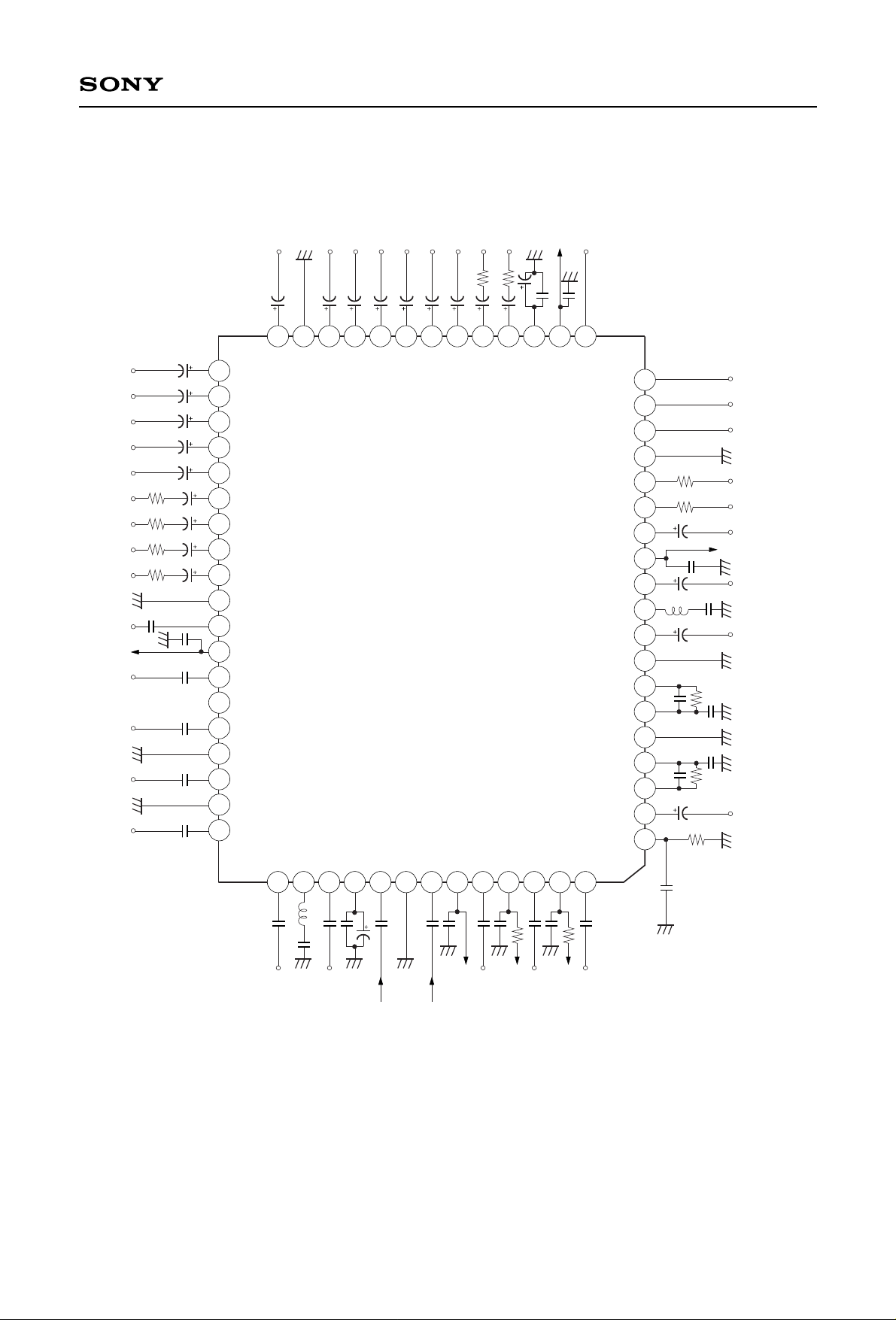
Application Diagram
REXT
TVOUT
RGD4
RGD3
LO0
RGD2
RGD1
LO1
CVOUT1
TRAP1
YOUT1
VVCC2
COUT1
SCL
SDA
ADR
MUTE
MODE1
MODE2
C2
NC
C3
VGND2
COUT2
TRAP2
YOUT2
DVCC
CVOUT2
DGND
LOUT2
ROUT2
LOUT1
ROUT1
RV1
RV2
RV3
RV4
RV5
RTV
AGND
LV1
LV2
LV3
LV4
LV5
LTV
ROUT3
LOUT3
ABIAS
AVCC
MODE3
C1
TRAP3
Y3
VBIAS
Y2
VGND1
Y1
VVCC1
CVIN2
TC2
CVIN1
TC1
TV
CXA2149Q
9V
20
21
22
23
24
25
26
27
28
29
30
31
32
33343536373839404142434445464748495051
0.1µ
0.1µ
10p
0.1µ
0.1µ
0.1µ
0.1µ
0.1µ
0.1µ
0.1µ
0.1µ
10µ
0.1µ
0.1µ
10µ
10µ
10µ
0.1µ
600
10µ
600
10µ
600
10µ
1µ
1µ
1µ
1µ
1µ
1µ 1µ
1µ 1µ 1µ 1µ 1µ 10µ
600
9V
9V
0.1µ
0.1µ
9V
68k
9V
68k
52
53
54
55
56
57
58
59
60
61
62
63
64
10µ
10p
10p
100p
10µ
10µ
0.1µ
0.1µ
0.1µ
39k
(1%)
220
560
10p
100p
560
220
600
10µ
10µ
0.1µ 0.1µ
600
1 2 3 4 5 6 7 8 9
10 11 12
13
14 15 16 17 18 19
Y2 DRIVE
Y1 DRIVE
180µ
180µ
9V
Application circuits shown are typical examples illustrating the operation of the devices. Sony cannot assume responsibility for
any problems arising out of the use of these circuits or for any infringement of third party patent and other right due to same.
Page 23

—23—
CXA2149Q
Applications Notes (see circuits diagram on next page).
1. Care should be taken with polarity sensitive capacitors. The respective bias voltages for audio and video
inputs and outputs are as follows.
C1, C2, C3, COUT1 and COUT2 are biased at approximately 4.5 V.
TV, CVIN1, CVIN2, Y1, Y2 and Y3 are SYNC tip clamped at approximately 3.9 V.
CVOUT1, CVOUT2, TVOUT have their SYNC tip output at approximately 3.5 V.
YOUT1, YOUT2 have their SYNC tip output at approximately 3.3 V.
ABIAS and VBIAS are equal to approximately 4.5 V.
2. Connect ADR to VCC when wishing to set the slave address to 92H.
3. Setting the MUTE pin to 2.5 V or more can mute the audio outputs.
4. TRAP1, TRAP2 and TRAP3 are set for a 3.58 MHz subcarrier. For a 4.43 MHz subcarrier typical values for
the two traps would be 47 µ and 27 p, respectively. Values may require adjustment dependent upon the
application. Each trap gives 6 dB’s of attenuation at the desired frequency.
5. LO0 and LO1 connected to ground when not required.
6. Connect all NC to ground in application.
Page 24
—24—
CXA2149Q
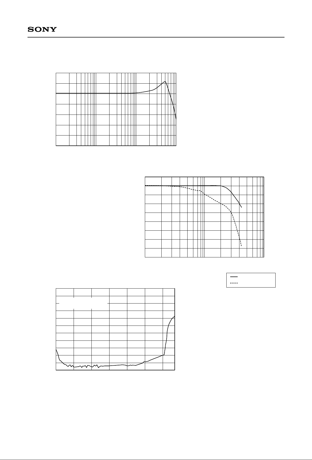
Typical audio system frequency response LTV-LOUT1
Frequency [Hz]
Audio system input/output gain [dB]
1000 10000 100000 1000000
4
2
0
–2
–4
–6
–8
–10
Video system typical frequency response
Frequency [MHz]
Video system input/output gain [dB]
1 10 100
8
4
6
2
0
–2
–4
–6
–10
–8
Typical audio system distortion vs. Input amplitude
Input amplitude [Vrms]
Total harmonic distortion [dB]
1.5 2 2.50.5 1 3
0
–40
–30
–20
–10
–50
–60
–70
–80
–90
–110
–100
f=1kHz
400Hz HPE, 80kHz LPF
TV-CVOUT1
Y1-CVOUT2 (Mx)
Example of Representative Characteristics
Page 25
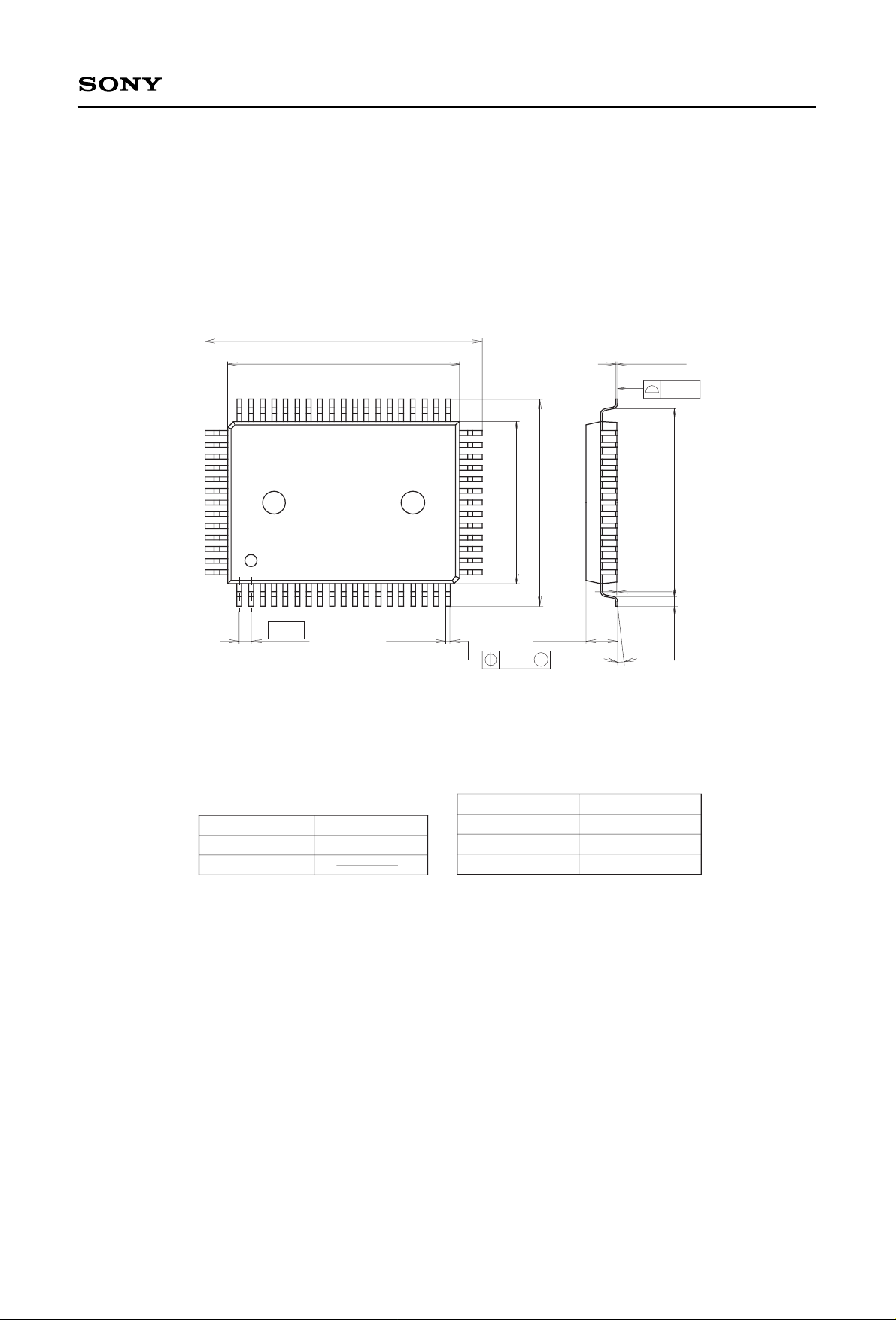
SONY CODE
EIAJ CODE
JEDEC CODE
23.9 ± 0.4
20.0 – 0.1
0.4 – 0.1
+ 0.15
14.0 – 0.1
1
19
20
32
33
51
52
64
0.15 – 0.05
+ 0.1
2.75 – 0.15
16.3
0.1 – 0.05
+ 0.2
0.8 ± 0.2
M
0.2
0.15
+ 0.4
17.9 ± 0.4
+ 0.4
+ 0.35
64PIN QFP(PLASTIC)
QFP-64P-L01
QFP064-P-1420
PACKAGE MATERIAL
LEAD TREATMENT
LEAD MATERIAL
PACKAGE MASS
EPOXY RESIN
SOLDER/PALLADIUM
42/COPPER ALLOY
PACKAGE STRUCTURE
PLATING
1.5g
1.0
0° to10°
Package Outline Unit : mm
CXA2149Q
—25—
 Loading...