

Page 1

LCD Signal Processor (Gamma Correction)
Description
The CXA2111R is a signal processor IC developed
for LCD panels. Gamma correction, gain and bias,
etc., can be adjusted using the I2C bus and external
adjustment pins. The output of this IC is ideal as the
input of the CXA2112R (LCD sample-and-hold
driver IC), and the sample-and-hold position, etc.,
can also be adjusted using the I2C bus.
CXA2111R
52 pin LQFP (Plastic)
Features
• Independent R, G and B gamma adjustment
• Three-point gamma gain and position adjustment
(one white side point, two black side points)
• Independent R, G and B output amplifier gain and
bias adjustment
• Various I2C bus-based controls and adjustment of
various characteristics by external DC input
• Input signal clamp function (variable clamp voltage)
• Black side limiter adjustment
• CXA2112R adjustment output
• Precharge output (for CXA2112R)
• High frequency response
• High slew rate output
Applications
• Liquid crystal projectors
• Compact liquid crystal monitors
Structure
Bipolar silicon monolithic IC
Absolute Maximum Ratings
• Supply voltage VCC –0.3 to +5.5 V
• Input voltage VI –0.3 to VCC + 0.3 V
• Storage temperature Tstg –65 to +150 °C
• Allowable power dissipation
PD 1000 mW
Operating Conditions
• Supply voltage VCC 4.75 to 5.25 V
• Digital input voltage high VH 2.2 to VCC V
• Digital input voltage low VL 0 to 0.8 V
• Operating temperature Topr –20 to +70 V
Sony reserves the right to change products and specifications without prior notice. This information does not convey any license by
any implication or otherwise under any patents or other right. Application circuits shown, if any, are typical examples illustrating the
operation of the devices. Sony cannot assume responsibility for any problems arising out of the use of these circuits.
– 1 –
E97448-PS
Page 2
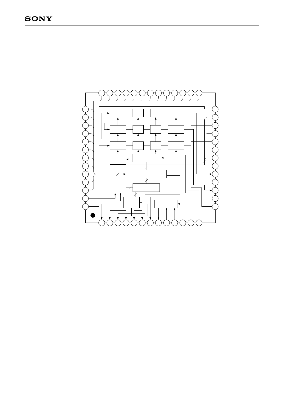
Pin Configuration and Block Diagram
GAMR_B2P
39
GAMG_B1P
GAMB_B1P
37
38
GAMB_WHP
GAMR_B1P
35
36
GAMR_WHP
GAMG_WHP
33
34
AMPGBIAS
AMPBBIAS
32
31
AMPBGAIN
AMPRBIAS
30
29
AMPRGAIN
AMPGGAIN
27
28
CXA2111R
GAMG_B2P BIN
GAMB_B2P CLPLEV
GAMR_WHG GIN
GAMG_WHG ATT
GAMB_WHG RIN
GAMR_B1G V
GAMG_B1G CLPPLS
GAMB_B1G GND
GAMR_B2G ROUT
GAMG_B2G PVCC
GAMB_B2G GOUT
40
41
42
43
44
45
46
47
48
49
50
SCL PGND
51
SDA BOUT
52
CLAMP DRIVERAMP
CLAMP DRIVERAMP
CLAMP DRIVERAMP
CLAMP
Control
Input
I/F
1
2
3
DLY_CNT
POS_CNT2
POS_CNT1
γ • AMP Adjust
Output
I/F
5
4
INV_CNT
DIR_CNT
γ
γ
γ
DAC/Control
6bit × 25
I2C Bus
6
7
SIDOUT
DATEST
PRG/SID
9
8
V33
SIDLEV
10
PRGPLS
11
PRGLEV
12
BLKLIM
13
23
20
18
16
GAMOFF
26
25
24
22
21
19
17
15
14
CC
– 2 –
Page 3
Pin Description
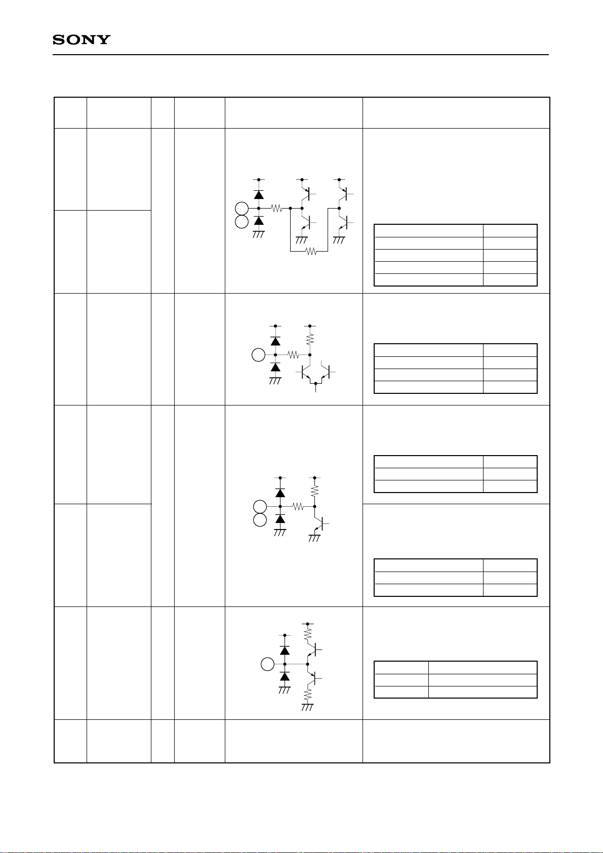
CXA2111R
Pin
No.
1
2
3
Symbol
POS_CNT1
POS_CNT2
DLY_CNT
I/O
O
O
Typical
pin voltage
0 to 5V
(4 value)
3 to 5V
Equivalent circuit
V
CC
1
2
300
VCC
300
3
VCC VCC
70k
VCC
25k
Description
CXA2112R control.
The sample-and-hold position is
determined by the I2C data.
POS_CNT1 is the low-order 4-value
output and POS_CNT2 is the highorder 4-value output for a total of 16value control.
I2C data input (2 bits)
00
01
10
11
Pin output
L
↓
↓
H
CXA2112R control.
The clock delay time is controlled by
output analog value using I2C data.
I2C data input (6 bits)
all 0
↓
all 1
Pin output
5V
↓
3V
4
5
6
DIR_CNT
INV_CNT
SIDOUT
O
(0V/5V)
2.3 to 3.3V
O
L/H
CXA2112R control.
The scan direction is determined by
the I2C data.
CC
300
VCC
20k
V
4
5
I2C data input (1 bit)
0
1
CXA2112R control.
Pin output
H
L
The clock polarity is determined by the
I2C data.
I2C data input (1 bit)
0
1
VCC
VCC
Pin output
H
L
Output for CXA2112R.
This pin outputs the precharge signal.
6
Pin 10 input
H
L
Pin 6 output
Level controlled by Pin 11
Level controlled by Pin 9
7
DATEST
DAC test output.
Set the I2C data to "1". This pin is
normally open.
– 3 –
Page 4
CXA2111R
Pin
No.
8
9
11
10
Symbol
V33
SIDLEV
PRGLEV
PRGPLS I
Typical
I/O
pin voltage
O
I
L: 0 to 0.8V
H: 2.2 to 5V
3.3V
0 to 5V
L/H
Equivalent circuit
VCC
8
VCC
9
11
10
VCC
50k
VCC
300
VCC
50k
75k
VCC
25µ
Description
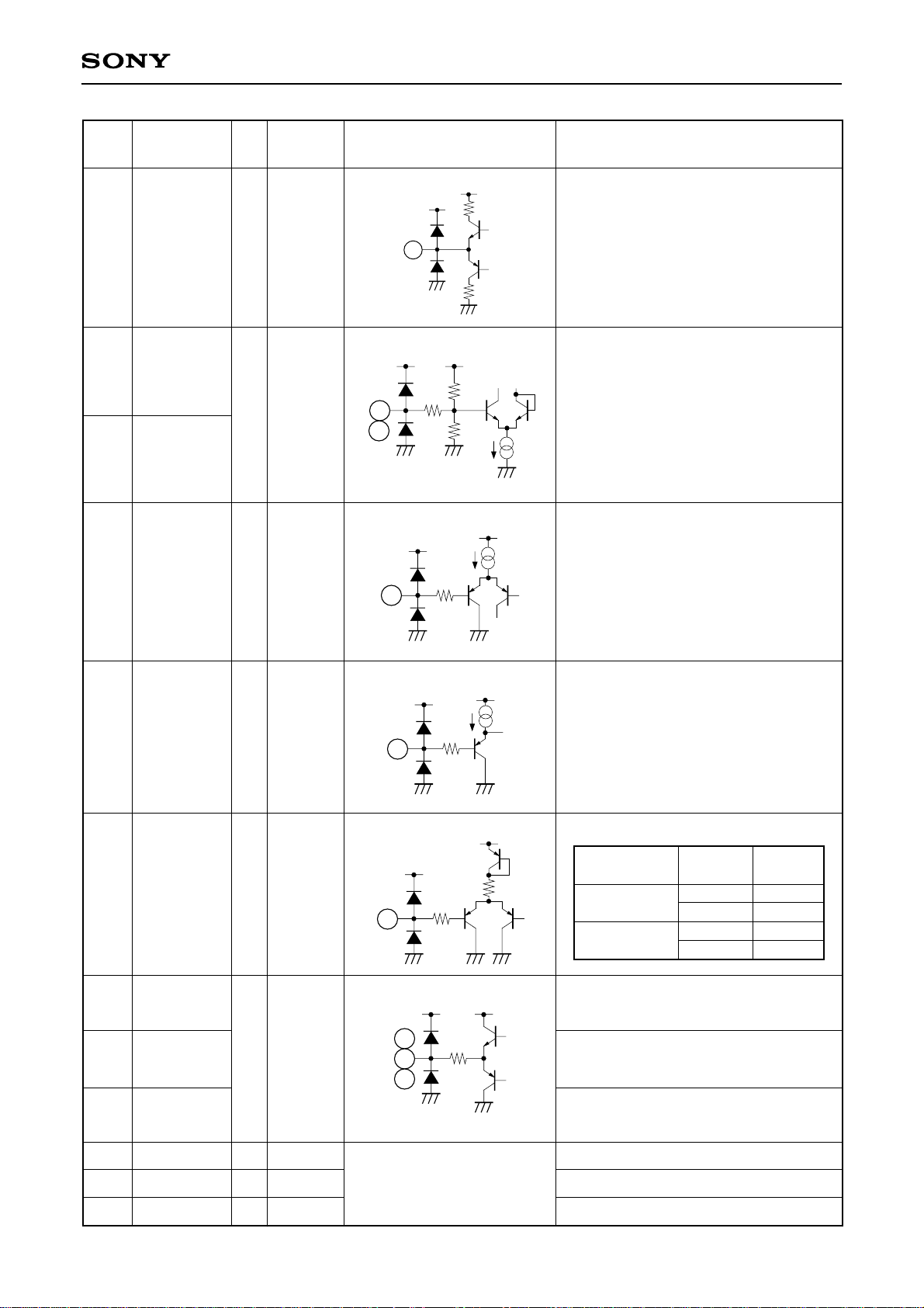
Output for CXA2112R.
This pin outputs 3.3V.
These pins determine the Pin 6 output
level.
See Pin 6.
100µ
This pin determines the Pin 6 output.
See Pin 6.
Set to low or high when using SIDOUT
(Pin 6) as a DC output.
BLKLIM
12
13
GAMOFF I
BOUT
14
GOUT
16
ROUT
18
I
1 to 5V
L: 0 to 0.8V
H: 2.2 to 5V
O
1.8 to 3.3V
L/H
13
12
18
14
16
VCC
VCC
PV
1.6k
300
CC
50
VCC
VCC
PVCC
GND
750µ
50k
Output black level (low level side) limit
voltage control.
Apply voltage of 1V DC or more.
Gamma characteristics ON/OFF setting.
I2C data input
(1bit)
0
1
Pin 13 input
H
L
H
L
γ mode
γ ON
γ OFF
γ OFF
γ OFF
B channel output.
G channel output.
R channel output.
15
17
19
PGND
PVcc
GND
GND
5V
GND
GND.
5V
GND.
– 4 –
Page 5
CXA2111R
Pin
No.
20
21
22
24
26
23
Symbol
CLPPLS
Vcc
RIN
GIN
BIN
ATT
Typical
I/O
pin voltage
I
L: 0 to 0.8V
H: 2.2 to 5V
5V
1.5 to 3.5V
I
I
L: 0 to 0.8V
H: 2.2 to 5V
L/H
L/H
Equivalent circuit
VCC
20
22
24
26
23
300
VCC
300
VCC
300
VCC
170µ
VCC
50µ
VCC
50µ
Description
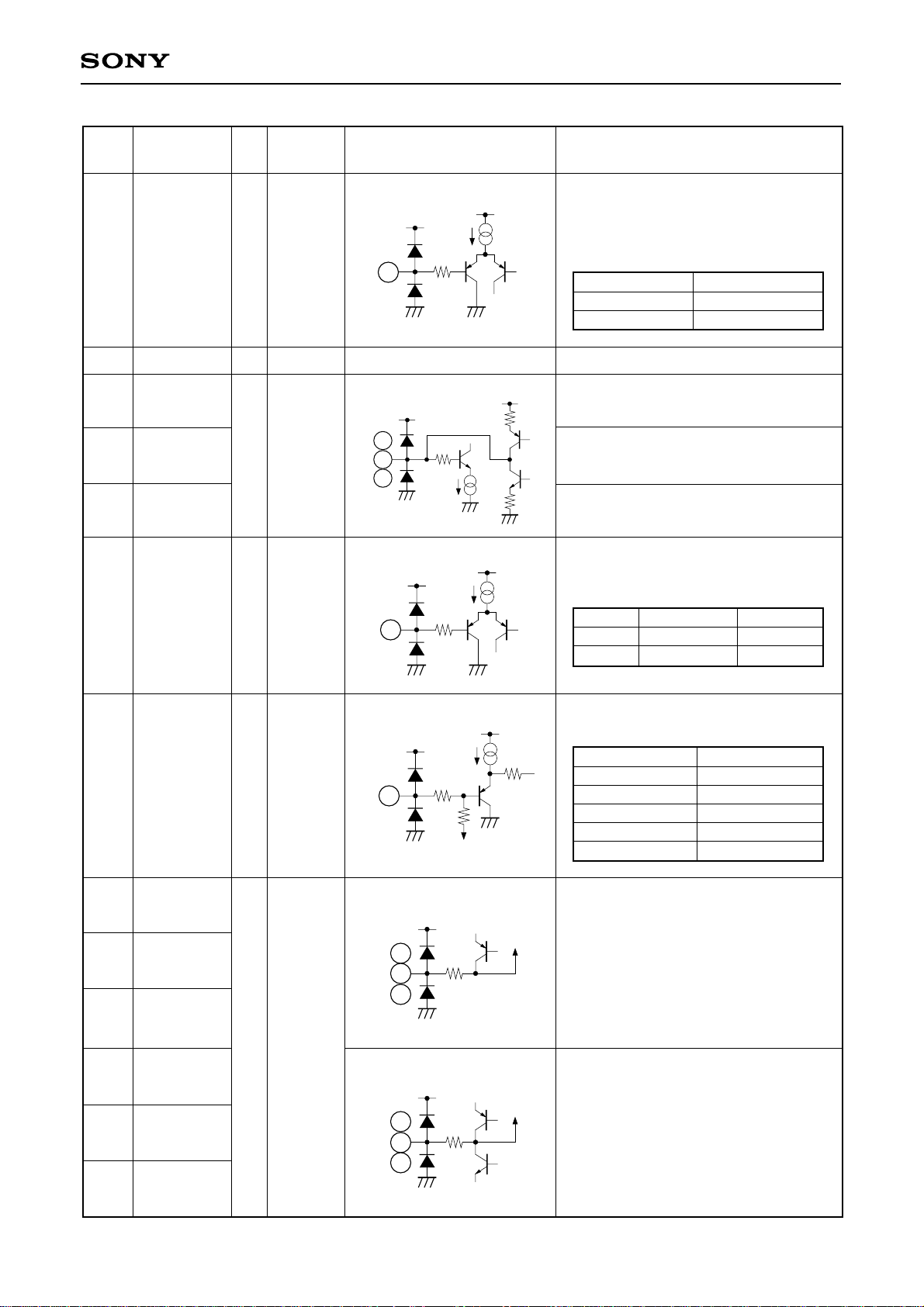
Input signal clamp pulse input.
Set to low when not using the clamp
function.
Pin input
H
L
Clamp function
ON
OFF
5V
R channel input.
G channel input.
B channel input.
Input signal gain control.
This pin also supports 2Vp-p input.
Pin input
H
L
Clamp block gain
0dB
–6dB
Signal level
For 1Vp-p
For 2Vp-p
25
27
28
29
30
31
32
CLPLEV
AMPRGAIN
AMPGGAIN
AMPBGAIN
AMPRBIAS
AMPGBIAS
AMPBBIAS
I
I
0 to 5V
0 to 5V
25
27
28
29
30
32
31
VCC
VCC
VCC
60k
20k
2.5V
25k
25k
VCC
50µ
2.5V
2.5V
Clamp voltage control during clamp
operation.
Pin input
5V
↓
2.5V (open)
↓
0V
Clamp voltage
2.5V
↓
2.0V
↓
1.5V
Amplifier gain control.
Independent control for R, G and B.
Equivalent to 2.5V input when open.
Amplifier bias control.
Independent control for R, G and B.
Equivalent to 2.5V input when open.
– 5 –
Page 6
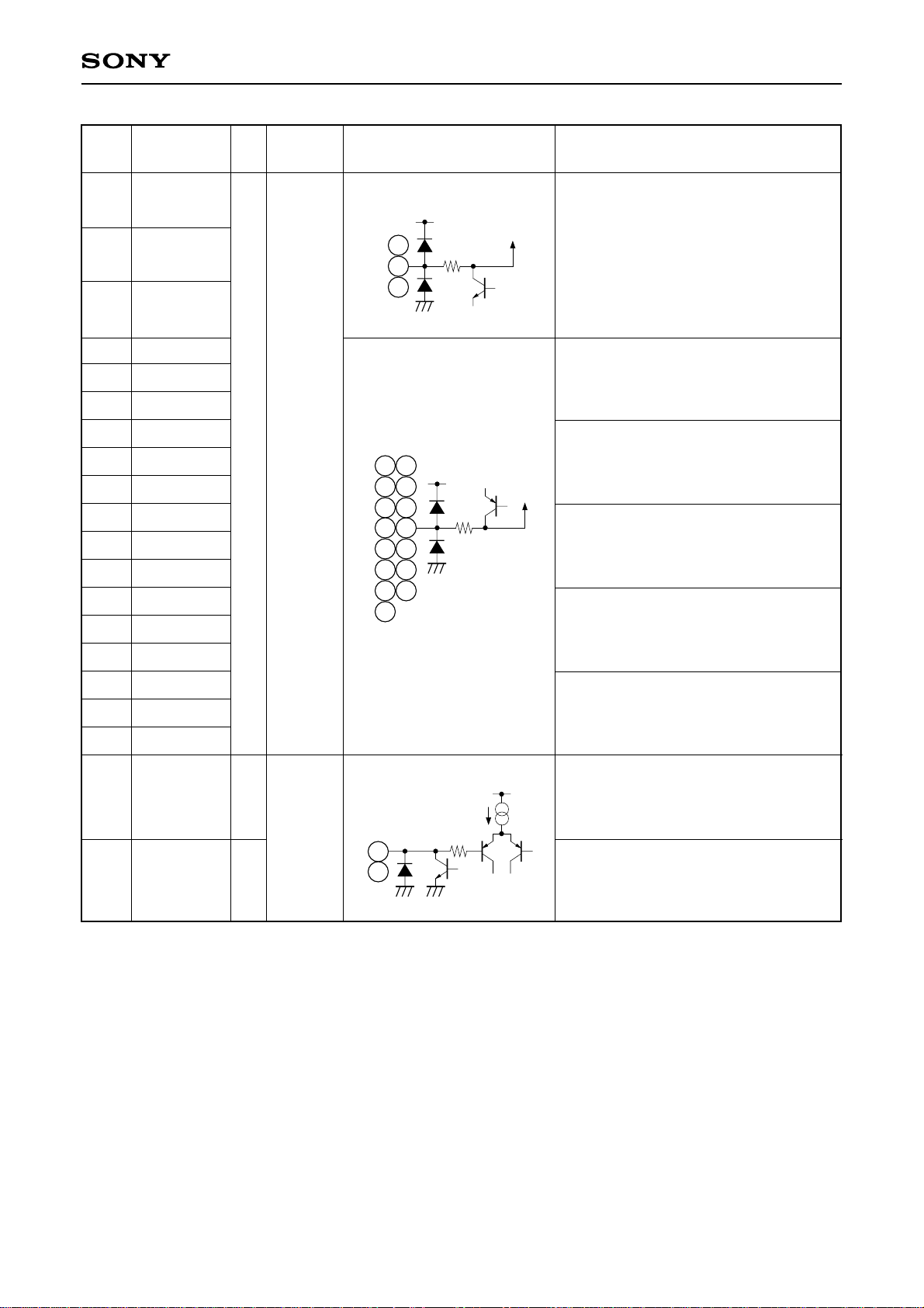
CXA2111R
Pin
No.
33
34
35
36
37
38
39
40
41
42
43
44
45
46
47
Symbol
GAMR_WHP
GAMG_WHP
GAMB_WHP
GAMR_B1P
GAMG_B1P
GAMB_B1P
GAMR_B2P
GAMG_B2P
GAMB_B2P
GAMR_WHG
GAMG_WHG
GAMB_WHG
GAMR_B1G
GAMG_B1G
GAMB_B1G
I/O
I
Typical
pin voltage
0 to 5V
Equivalent circuit
VCC
33
34
35
43
44
45
46
47
48
49
50
36
37
38
39
40
41
42
25k
VCC
25k
2.5V
2.5V
Description
Gamma white position control.
Independent control for R, G and B.
Equivalent to 2.5V input when open.
Gamma black 1 position control.
Independent control for R, G and B.
Equivalent to 2.5V input when open.
Gamma black 2 position control.
Independent control for R, G and B.
Equivalent to 2.5V input when open.
Gamma white gain control.
Independent control for R, G and B.
Equivalent to 2.5V input when open.
Gamma black 1 gain control.
Independent control for R, G and B.
Equivalent to 2.5V input when open.
48
49
50
51
52
GAMR_B2G
GAMG_B2G
GAMB_B2G
SCL
SDA
I/O
I
L/H
(0V/5V)
51
52
Gamma black 2 gain control.
Independent control for R, G and B.
Equivalent to 2.5V input when open.
VCC
I2C bus clock input.
50µ
4k
I2C bus data input.
– 6 –
Page 7

I2C Bus Format
Slave address: 0111 0110 (76h)
CXA2111R
Sub address bit7 bit1 bit0
∗∗∗00000 (00h)
∗∗∗00001 (01h)
∗∗∗00010 (02h)
∗∗∗00011 (03h)
∗∗∗00100 (04h)
∗∗∗00101 (05h)
∗∗∗00110 (06h)
∗∗∗00111 (07h)
∗∗∗01000 (08h)
∗∗∗01001 (09h)
∗∗∗01010 (0Ah)
∗∗∗01011 (0Bh)
∗∗∗01100 (0Ch)
∗∗∗01101 (0Dh)
∗∗∗01110 (0Eh)
∗∗∗01111 (0Fh)
bit6 bit5 bit4 bit3 bit2
AMPRGAIN
AMPGGAIN
AMPBGAIN
AMPRBIAS
AMPGBIAS
AMPBBIAS
GAMR_WHP
GAMG_WHP
GAMB_WHP
GAMR_B1P
GAMG_B1P
GAMB_B1P
GAMR_B2P
GAMG_B2P
GAMB_B2P
GAMR_WHG
∗∗∗10000 (10h)
∗∗∗10001 (11h)
∗∗∗10010 (12h)
∗∗∗10011 (13h)
∗∗∗10100 (14h)
∗∗∗10101 (15h)
∗∗∗10110 (16h)
∗∗∗10111 (17h)
∗∗∗11000 (18h)
GAMG_WHG
GAMB_WHG
GAMR_B1G
GAMG_B1G
GAMB_B1G
GAMR_B2G
GAMG_B2G
GAMB_B2G
DLY_CNT
GAMOFF
POS_CNT2
POS_CNT1
DIR_CNT
DATEST
INV_CNT
– 7 –
Page 8
CXA2111R
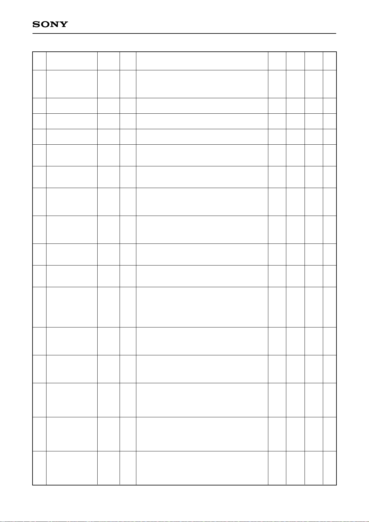
Electrical Characteristics (See the Electrical Characteristics Measurement Circuit.) (VCC, PVCC = 5V, Ta = 25°C)
No. Item Symbol
Current
1
consumption
Digital input
2
voltage high
Digital input
3
voltage low
Maximum input
4
voltage amplitude
Maximum output
5
voltage amplitude
Gamma white gain
6
max.
Gamma black 1
7
gain max.
Gamma black 2
8
gain max.
9
Amplifier gain max.
10
Amplifier gain min.
Icc
Vih
Vil
Vix
Vox
Ggwx
Ggb1x
Ggb2x
Gax
Gan
Amplifier bias
11
output variable
Vab
range
Gamma white gain
12
2
I
C max.
Gamma white gain
13
I2C min.
Gamma black 1
14
15
16
2
gain I
C max.
Gamma black 1
2
gain I
C min.
Gamma black 2
2
gain I
C max.
Ggwxi
Ggwni
Ggb1xi
Ggb1ni
Ggb2xi
Measurement
point
I21
V14
V16
V18
V14
V16
V18
V14
V16
V18
V14
V16
V18
V14
V16
V18
V14
V16
V18
V14
V16
V18
V14
V16
V18
V14
V16
V18
V14
V16
V18
V14
V16
V18
V14
V16
V18
Measurement conditions and measurement outline Min. Typ. Max.
[Gamma gain (white, black 1, black 2) = max.,
amplifier gain = max.]
V22, 24, and 26 = 2.5V, V27 to 29 and 42 to 50 =
80
135
180
5V, V30 to 41 = open, Measure the I21 current.
Excluding the I
Excluding the I
Pins 22, 24 and 26 input
Pins 14, 16 and 18 output
2
C bus pins (Pins 51 and 52).
2
C bus pins (Pins 51 and 52).
2.2
GND
2
1.5
Vcc
0.8
V27 to 29 and 36 to 44 = 5V, V30 to 35 = open, V45 to 50 = 0V
Calculate Vwx/Vo (a) for the maximum Vwx at Vo (e),
6.0
7.4
9.2
Vo (f) and Vo (g).
V27 to 29, 39 to 41 and 45 to 47 = 5V, V30 to 32 and
36 to 38 = open, V33 to 35, 42 to 44 and 48 to 50 = 0V.
Calculate Vb1x/Vo (i) for the maximum Vb1x at Vo (c),
8.0
9.5
11.6
Vo (d) Vo (e) and Vo (f).
V27 to 29, 36 to 38 and 48 to 50 = 5V, V30 to 32 =
3.75V, V33 to 35 and 42 to 47 = 0V, V39 to 41 = 3.3V
Calculate Vb2x/Vo (h) for the maximum Vb2x at Vo (a),
16.0
19.7
26.8
Vo (b) and Vo (c).
V13 = 0V, V27 to 29 = 0V, V30 to 50 = open
Calculate Vo (j)/0.1.
V13 = 0V, V27 to 29 = 5V, V30 to 50 = open
Calculate Vo (j)/0.1.
1.65
0.28
2.26
0.35
3.25
0.46
V13 = 0V, V22, 24 and 26 = 2.5V,
V27 to 29 = 0.75V, V33 to 50 = open
V14, 16 and 18 voltages when V30 to 32 = 0V,
open and 5V.
±0.80
±0.96
±1.15
Calculate Vb (0V) – Vb (open) and Vb (5V) – Vb
(open) at Vb (0V), Vb (open) and Vb (5V).
V27 to 29 and 36 to 44 = 5V, V30 to 35 and 42 to
44 = open, V45 to 50 = 0V, I
Calculate Vwxi/Vo (a) for the maximum Vwxi at
2
C data = 3Fh
5.85
7.21
8.65
Vo (e), Vo (f) and Vo (g).
V27 to 29 and 36 to 44 = 5V, V30 to 35 and 42 to
44 = open, V45 to 50 = 0V, I2C data = 00h
Calculate Vwni/Vo (a) for the maximum Vwni at
3.80
4.71
5.65
Vo (e), Vo (f) and Vo (g).
V27 to 29, 39 to 41 and 45 to 47 = 5V, V30 to 32,
36 to 38 and 45 to 47 = open, V33 to 35, 42 to 44
and 48 to 50 = 0V, I
2
C data = 3Fh
7.6
9.11
10.7
Calculate Vb1xi/Vo (i) for the maximum Vb1xi at
Vo (c), Vo (d) Vo (e) and Vo (f).
V27 to 29, 39 to 41 and 45 to 47 = 5V, V30 to 32,
36 to 38 and 45 to 47 = open, V33 to 35, 42 to 44
and 48 to 50 = 0V, I
2
C data = 00h
5.05
6.02
7.00
Calculate Vb1ni/Vo (i) for the maximum Vb1ni at
Vo (c), Vo (d) Vo (e) and Vo (f).
V27 to 29, 36 to 38 and 48 to 50 = 5V, V30 to 32 =
3.75V, V33 to 35 and 42 to 47 = 0V, V39 to 41 =
3.3V, V48 to 50 = open, I
2
C data = 3Fh
15.8
19.5
23.2
Calculate Vb2xi/Vo (h) for the maximum Vb2xi at
Vo (a), Vo (b) and Vo (c).
Unit
mA
V
V
V
V
times
times
times
times
times
V
times
times
times
times
times
– 8 –
Page 9
CXA2111R
No.
17
18
19
Item Symbol
Gamma black 2
2
C min.
gain I
Amplifier gain
I2C max.
Amplifier gain
2
C min.
I
Amplifier bias I
output variable
20
range
Frequency
21
response
Clamp voltage
22
min.
Clamp voltage
23
max.
Black limiter
24
voltage
Output maximum
voltage value
25
(white limiter voltage)
SIDOUT output min.
26
SIDOUT output max.
27
I2C DAC (6-bit)
28
DLE
Output rise/fall
time
29
<Reference data>
Gamma position max.
(white/black 1/black 2)
30
<Reference data>
Gamma position min.
(white/black 1/black 2)
31
<Reference data>
Gamma position
2
C max. (white)
I
32
<Reference data>
Gamma position
2
C min. (white)
I
33
<Reference data>
Gamma position I2C
max. (black 1/black 2)
34
<Reference data>
Gamma position I2C
min. (black 1/black 2)
35
<Reference data>
Measurement
point
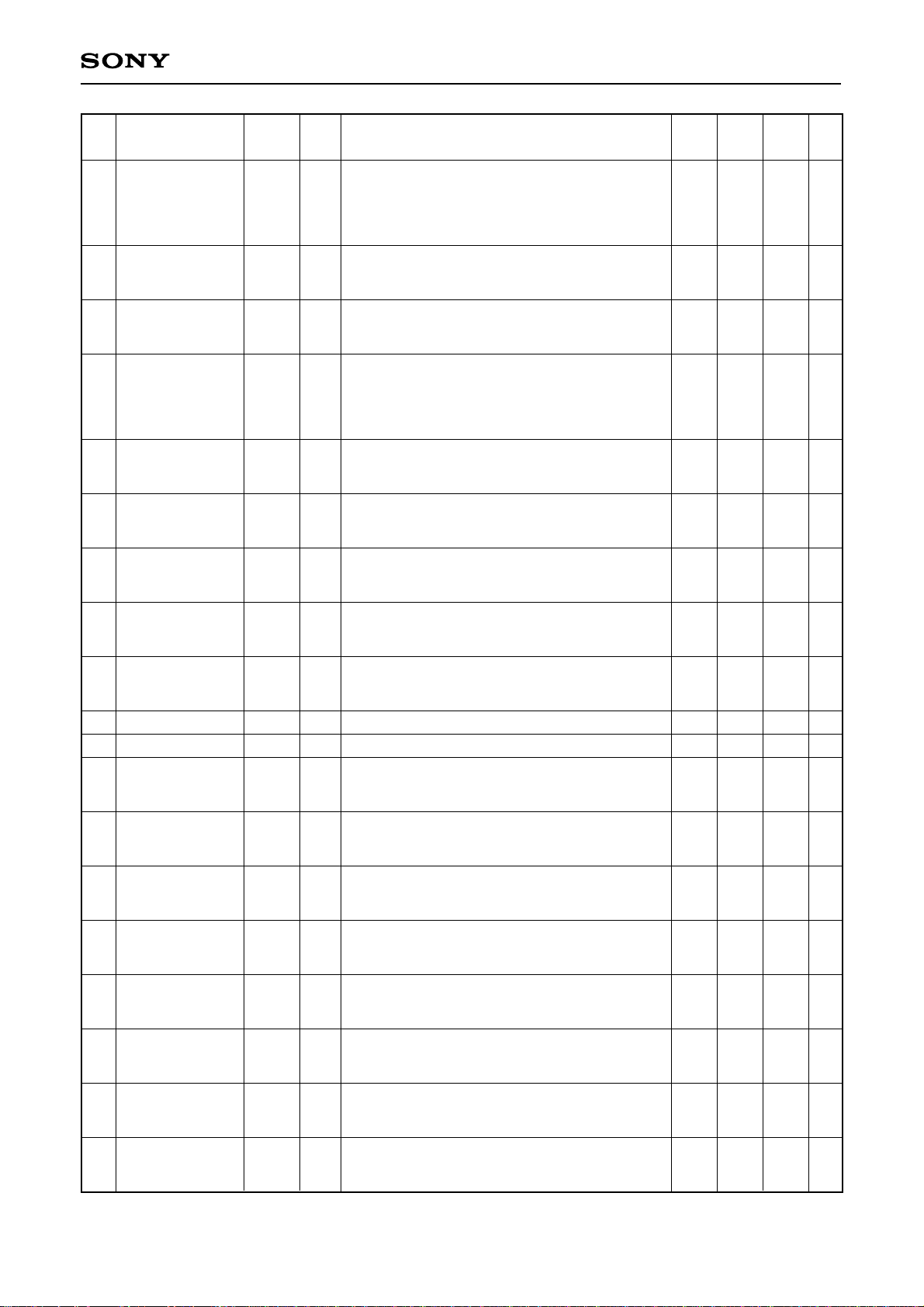
Measurement conditions and measurement outline Min. Typ. Max.
Unit
V27 to 29, 36 to 38 and 48 to 50 = 5V, V30 to 32 =
3.75V, V33 to 35 and 42 to 47 = 0V, V39 to 41 =
Ggb2ni
V14
3.3V, V48 to 50 = open, I
V16
Calculate Vb2xi/Vo (h) for the maximum Vb2xi at
V18
2
C data = 3Fh
11.3
14.0
16.7
times
Vo (a), Vo (b) and Vo (c).
V14
Gaxi
Gani
2
C
Vabi
V13 = 0V, V27 to 50 = open, I
V16
Calculate Vo (j)/0.1.
V18
V14
V13 = 0V, V27 to 50 = open, I
V16
Calculate Vo (j)/0.1.
V18
V13 = 0V, V22, 24 and 26 = 2.5V, V27 to 29 = 0.75V,
V30 to 50 = open
V14
V14, 16 and 18 voltages when I
V16
Calculate Vbi (00h) – Vbi (20h) and Vbi (3Fh) –
V18
2
C data = 00h
2
C data = 3Fh
2
C data = 00h, 20h and 3Fh.
0.44
0.30
±0.34
0.55
0.39
±0.39
0.67
0.47
±0.45
times
times
V
Vbi (20h) at Vbi (00h), Vbi (20h) and Vbi (3Fh).
[Gamma OFF, amplifier gain min., ratio of 100MHz to 20MHz]
V14
Gf
Vcn
Vcx
Vbl
Vwl
Vsn
Vsx
V13 = 0V, V27 to 29 = 5V, V30 to 50 = open
V16
Calculate 20∗LOG {Vo (k)/Vo (j)}.
V18
Vr
SW22, 24, 26 = b, SW25 = ON
Vg
V20 = 5V, V25 = 0V
Vb
Vr
SW22, 24, 26 = b, SW25 = ON
Vg
V20 = 5V, V25 = 5V
Vb
V14
V12 = 1.3V, V13 = 0V, V22, 24, 26 = 2V,
V16
V27 to 29 = 0.75V, V30 to 32 = 0V, V33 to 50 = open
V18
V14
V13, 27 to 29 = 0V, V22, 24, 26 = 3.1V,
V16
V30 to 32 = 5V, V33 to 50 = open
V18
V9 = V11 = 0.5 V, V10 = 0V or 5V
V6
V9 = V11 = 4.5 V, V10 = 0V or 5V
V6
–2.7
1.35
2.75
1.00
3.50
1.75
3.30
1.45
2.85
1.19
3.71
1.98
3.48
1.55
2.95
1.35
4.00
2.15
3.65
dB
V
V
V
V
V
V
DAC output when DAC data = 00h, 1Fh, 20h and 3Fh.
Dle
Trf
Pgx
Pgn
Pgwxi
Pgwni
Pgbxi
Pgbni
Calculate | {V (20h) – V (1Fh)}/[{V (3Fh) – V (00h}/63] |
–
1 at V (00h), V (1Fh), V (20h) and V (3Fh).
V14
Gamma OFF, gain adjusted so that 1Vp-p pulse
V16
input results in 1.5Vp-p output, output 3pF load
V18
With input DC 2.0 to 3.0V set as 0 to 100 IRE
V33 to V41 = 0V
With input DC 2.0 to 3.0V set as 0 to 100 IRE
V33 to V41 = 5V
With input DC 2.0 to 3.0V set as 0 to 100 IRE
V33 to 35 = open, I2C data = 3Fh
With input DC 2.0 to 3.0V set as 0 to 100 IRE
V33 to 35 = open, I
With input DC 2.0 to 3.0V set as 0 to 100 IRE
V36 to 41 = open, I
With input DC 2.0 to 3.0V set as 0 to 100 IRE
V36 to 41 = open, I
2
C data = 00h
2
C data = 00h
2
C data = 3Fh
–0.9
4
100
100
40
70
0
0.6
0
LSB
ns
IRE
IRE
IRE
IRE
IRE
IRE
– 9 –
Page 10
V27
V28V29V30V31V32V33V34V35V36V37V38V39
Vr
Vb
Vg
AMPRGAIN
2728
AMPGGAIN
AMPBGAIN
29
0.1µ
V26
b
BIN
CXA2111R
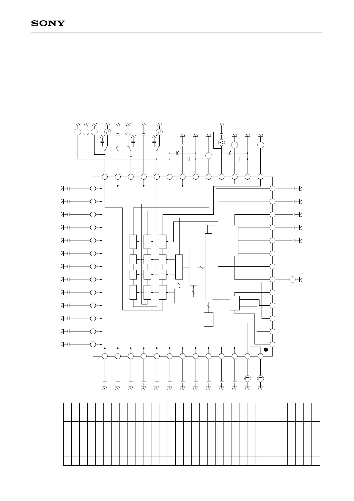
(a) 2.15Vdc + 0.1Vp-p 20MHz
(b) 2.25Vdc + 0.1Vp-p 20MHz
(c) 2.35Vdc + 0.1Vp-p 20MHz
(d) 2.45Vdc + 0.1Vp-p 20MHz
(e) 2.55Vdc + 0.1Vp-p 20MHz
(f) 2.65Vdc + 0.1Vp-p 20MHz
(g) 2.75Vdc + 0.1Vp-p 20MHz
(h) 2.85Vdc + 0.1Vp-p 20MHz
(i) 2.95Vdc + 0.1Vp-p 20MHz
(j) 2.5Vdc + 0.1Vp-p 20MHz
V13
GAMOFF
V12
BLKLIM
PRGLEV
(k) 2.5Vdc + 0.1Vp-p 100MHz
In addition, the V14, 16 and 18
output levels for the above inputs
(x) are labeled Vo (x).
5V
1V
V11V10V9
The following sine wave signals
are defined as the V22, 24 and
26 inputs.
V23 5V
ATT
23
V22
0.1µ
b
RIN
22
to CLAMP
Control
SW22
a
V21 5V
47µ/16V
V20 0V
CLPPLS
20
to CLAMP
0.1µ
GND
19
Control
CC
V
21
I21
V18
ROUT
18
V16
47µ/16V
CC
PV
17
0.1µ
GOUT
16
PGND
15
V14
BOUT
14
13
12
11
V24
V25 5V
SW26
SW24
a
CLPLEV
25
26
a
SW25
GIN
24
to CLAMP
Control
0.1µ
b
AMPRBIAS
30
AMPGBIAS
31
AMPBBIAS
32
GAMR_WHP
33
GAMG_WHP
34
GAMB_WHP
35
GAMR_B1P
36
GAMG_B1P
37
GAMB_B1P
38
GAMR_B2P
39
GAMG_B2P
to DAC/Control
41
40
GAMB_B2P
V40
GAMR_WHG
V41
γ
CLAMP DRIVERAMP
42
V42
γ
CLAMP DRIVERAMP
43
GAMB_WHG
GAMG_WHG
V43
44
V44
γ
CLAMP DRIVERAMP
to DAC/Control
45
GAMR_B1G
γ • AMP Adjust
Control
CLAMP
GAMG_B1G
V45
46
DAC/Control
GAMB_B1G
V46
47
6bit × 25
Input
GAMR_B2G
V47
C Bus
2
I
I/F
48
GAMG_B2G
V48
49
Output
GAMB_B2G
V49
PRG/SID
I/F
50
V50
SCL
51
2
C input
I
(clock)
V51
SDA
52
C input
2
I
(data)
V52
PRGPLS
10
SIDLEV
9
V33
8
DATEST
7
6
SIDOUT
V6
INV_CNT
5
DIR_CNT
4
DLY_CNT
3
2
1
POS_CNT2
POS_CNT1
00h
00h
00h
20h
20h
20h
00h
00h
00h
00h
Data
00h
Item
AMPRGAIN
AMPGGAIN
AMPBGAIN
AMPRBIAS
AMPGBIAS
AMPBBIAS
GAMR_WHP
GAMG_WHP
GAMB_WHP
GAMR_B1P
C standard data>
2
<I
Slave address = 76h
1
2
3
4
5
6
7
Electrical Characteristics Measurement Circuit
No.
8
GAMG_B1P
9
101112131415161718192021222324252627282930
00h
00h
00h
GAMB_B1P
GAMR_B2P
GAMG_B2P
– 10 –
00h
00h
00h
GAMB_B2P
GAMR_WHG
GAMG_WHG
00h
00h
00h
GAMB_WHG
GAMR_B1G
GAMG_B1G
00h
00h
00h
GAMB_B1G
GAMR_B2G
GAMG_B2G
00
00h
00h
GAMB_B2G
DLY_CNT
POS_CNT1
0
0
00
POS_CNT2
DIR_CNT
INV_CNT
0
1
GAMOFF
DATEST
31
Page 11

CXA2111R
Description of Operation
1. Gamma control
The bend positions and respective gains of one
white side point and two black side points can be
varied.
Control is performed independently for R, G and B
Black 1 position
White gain
Gamma
OFF
White position
by the I2C bus or by external DC.
In addition, the gamma function can easily be
Black 2 position
Black 1 gain
forced OFF (by Pin 13 or the I2C bus).
Black 2 gain
2. Amplifier gain and bias control
After adjusting the gamma, the signal gain and DC voltage can also be adjusted.
3. SIDOUT
SIDOUT generates the precharge signal.
After the CXA2111R determines the DC level (Pins 9 and 11) and the pulse width (Pin 10), the signal is
inverted by the CXA2112R and applied to the LCD panel.
See the Example of Representative Characteristics for the DC level.
PRGPLS input
(Pin 10)
Voltage determined by Pin 9
SIDOUT output
(Pin 6)
Voltage determined by Pin 11
Output example
4. I2C bus
The various gamma and amplifier controls can be performed in accordance with the I2C Bus Format table.
In addition, the sample-and-hold position and other items can also be controlled by connecting the
CXA2112R.
– 11 –
Page 12
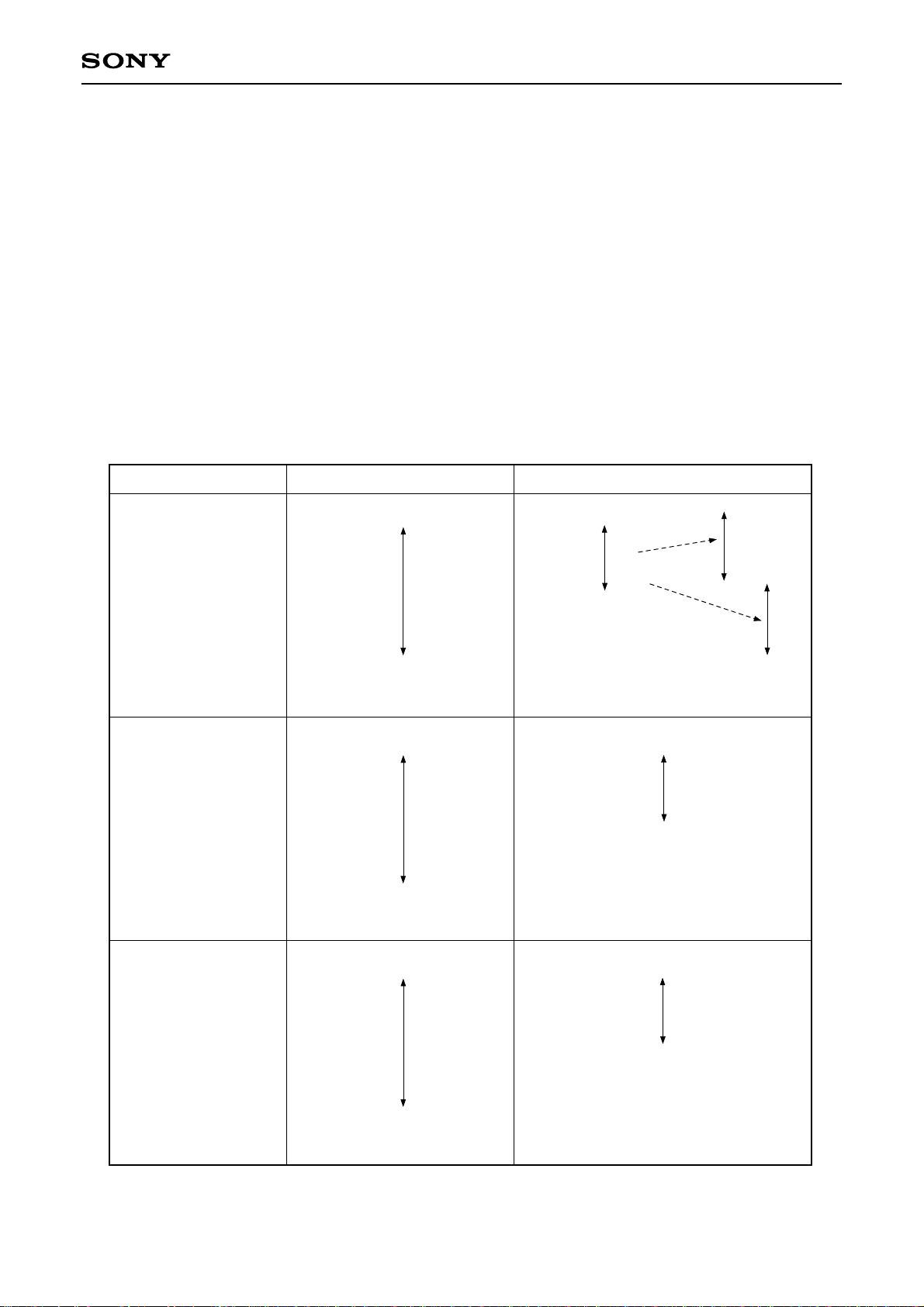
Notes on Operation
1. External DC voltage adjustment, I2C adjustment and variable ranges
(a) When varying the external DC voltage
Setting the I2C data to the standard setting values (listed in the Electrical Characteristics Measurement
Circuit) is recommended when performing the various adjustments using the external pins (Pins 27 to 50).
Note that setting data that differs from these standard setting values may clip one side of the variable
ranges below.
(b) When varying the I2C setting
The variable ranges when the external pins are open or 2.5V are as shown in the table below. The I2C
variable range position can be altered by changing the voltage applied to the external pins. However, note
that characteristics in excess of the range in (a) above cannot be obtained.
CXA2111R
γ white gain
γ black 1 gain
(a) External voltage adjustment
× 7.4
× 1
5V
0V
(I2C standard setting 00h)
× 9.5
× 1
5V
0V
(I2C standard setting 00h)
(b) I2C adjustment (external pins open or 2.5V)
× 7.21
3Fh
× 4.71 00h
The variable position can be altered
by changing the external voltage.
× 9.11
× 6.02
3Fh
00h
γ black 2 gain
× 19.7
× 1
5V
0V
(I2C standard setting 00h)
– 12 –
× 19.5
× 14.0
3Fh
00h
Page 13

CXA2111R
γ white position
γ black 1 position
(a) External voltage adjustment
100 IRE
0 IRE
0V
5V
(I2C standard setting 00h)
100 IRE
0 IRE
0V
5V
(I2C standard setting 00h)
(b) I2C adjustment (external pins open or 2.5V)
100 IRE
40 IRE
70 IRE
0 IRE
3Fh
00h
00h
3Fh
100 IRE
0V
70 IRE
00h
γ black 2 position
0 IRE
5V
0 IRE
3Fh
(I2C standard setting 00h)
Note) The 0 to 100 IRE levels here correspond to the following values when ATT (Pin 23) is high.
Clamp OFF: Input 2 to 3V (1Vp-p)
Clamp ON: Input 1Vp-p (however, Pin 25 = open or 2.5V)
– 13 –
Page 14
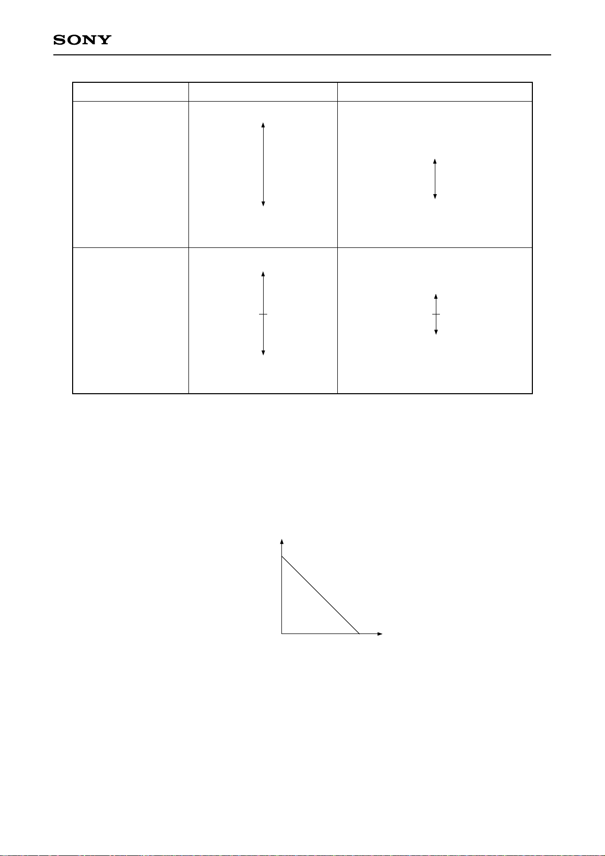
CXA2111R
Amplifier gain
Amplifier bias
(relative variation)
(a) External voltage adjustment
× 2.26
× 0.35
0V
5V
(I2C standard setting 00h)
+0.96V
0V
–0.96V
5V
2.5V
0V
(I2C standard setting 20h)
(b) I2C adjustment (external pins open or 2.5V)
× 0.55
× 0.39
+0.39V
0V
–0.39V
00h
3Fh
00h
20h
3Fh
2. Input signal level and clamp
Set Pin 23 (ATT) low when the input amplitude exceeds 1Vp-p (up to 2Vp-p).
In this case, care should be taken for the clamp voltage setting (Pin 25) when applying the clamp. See the
figure below.
(The input pin voltage should not exceed the range of 1.5V DC to 3.5V DC.)
Pin 25 setting voltage range
2.5Vdc ± 2.5V
(0 to 5V)
2.5Vdc ± 0V
1Vp-p 2Vp-p
Input level
3. I2C bus
The CXA2111R requires I2C bus control.
The initial values must be set after power-on even when using only external DC adjustment.
– 14 –
Page 15
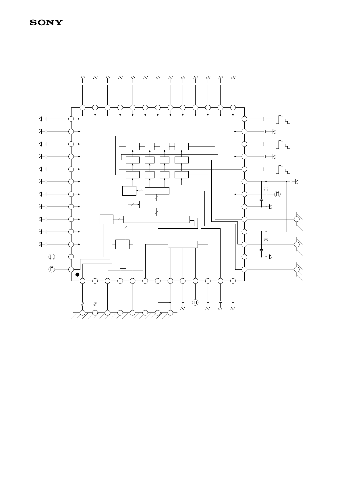
Application Circuit
CXA2111R
2
C bus
I
(clock)
2
C bus
I
(data)
GAMG_B2P
GAMB_B2P
GAMR_WHG
GAMG_WHG
GAMB_WHG
GAMR_B1G
GAMG_B1G
GAMB_B1G
GAMR_B2G
GAMG_B2G
GAMB_B2G
SCL
SDA
40
41
42
43
44
45
46
47
48
49
50
51
52
15k∗15k
GAMR_B2P
39
to DAC/Control
1
POS_CNT1
∗
1
GAMB_B1P
38
Input
I/F
2
POS_CNT2
2
GAMG_B1P
37
Output
3
DLY_CNT
13
49
GAMB_WHP
GAMR_B1P
36
CLAMP
Control
I/F
4
DIR_CNT
CXA2112R
GAMG_WHP
35
34
CLAMP DRIVERAMP
CLAMP DRIVERAMP
CLAMP DRIVERAMP
6
5
SIDOUT
INV_CNT
52
39
GAMR_WHP
33
to DAC/Control
γ
γ
γ
γ • AMP Adjust
DAC/Control
6bit × 25
I2C Bus
7
DATEST
42
AMPBBIAS
32
PRG/SID
8
V33
48
AMPGBIAS
31
30
9
10
SIDLEV
AMPRBIAS
29
11
PRGPLS
AMPGGAIN
AMPBGAIN
12
BLKLIM
PRGLEV
AMPRGAIN
2728
to CLAMP
Control
to CLAMP
Control
to CLAMP
Control
13
GAMOFF
26
25
24
23
22
21
20
19
18
17
16
15
14
BIN
CLPLEV
GIN
ATT
RIN
V
CC
CLPPLS
0.1µ
GND
ROUT
PV
CC
GOUT
0.1µ
PGND
BOUT
0.1µ
0.1µ
0.1µ
47µ/16V
Clamp
pulse
47µ/16V
5V
47
47
47
CXA2112R
∗
When using two CXA2112R, connect the ICs directly
without inserting resistors.
Application circuits shown are typical examples illustrating the operation of the devices. Sony cannot assume responsibility for
any problems arising out of the use of these circuits or for any infringement of third party patent and other right due to same.
– 15 –
Page 16
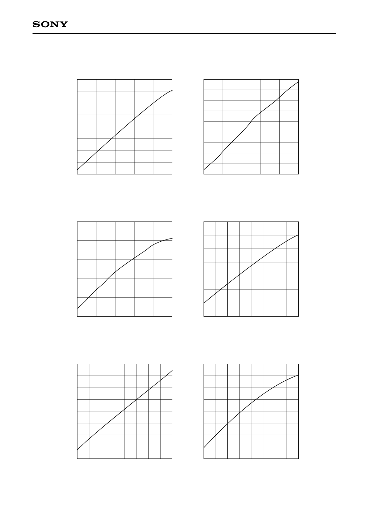
Example of Representative Characteristics (Vcc = 5V, Ta = 25°C)
CXA2111R
9
8
7
6
5
Gain [times]
4
3
2
1
0
25
20
R/G/B gamma white gain
2
(I
C: standard setting)
12345
Control pin voltage (Pins 42, 43 and 44) [V]
R/G/B gamma black 2 gain
2
(I
C: standard setting)
R/G/B gamma black 1 gain
2
(I
C: standard setting)
10
9
8
7
6
5
Gain [times]
4
3
2
1
0
12345
Control pin voltage (Pins 45, 46 and 47) [V]
R/G/B gamma white gain I2C characteristics
(Control pins = open)
8.0
7.5
7.0
15
10
Gain [times]
5
0
012345
Control pin voltage (pins 48, 49 and 50) [V]
R/G/B gamma black 1 gain I2C characteristics
(Control pins = open)
9.5
9.0
8.5
8.0
7.5
Gain [times]
7.0
6.5
6.5
6.0
Gain [times]
5.5
5.0
4.5
00
10 20 30
08 18 28 38 3F
2
I
C setting [HEX]
R/G/B gamma black 2 gain I2C characteristics
(Control pins = open)
21
20
19
18
17
Gain [times]
16
15
6.0
5.5
08 18 28 38 3F
00
10 20 30
2
C setting [HEX]
I
– 16 –
14
13
08 18 28 38 3F
00
10 20 30
2
C setting [HEX]
I
Page 17
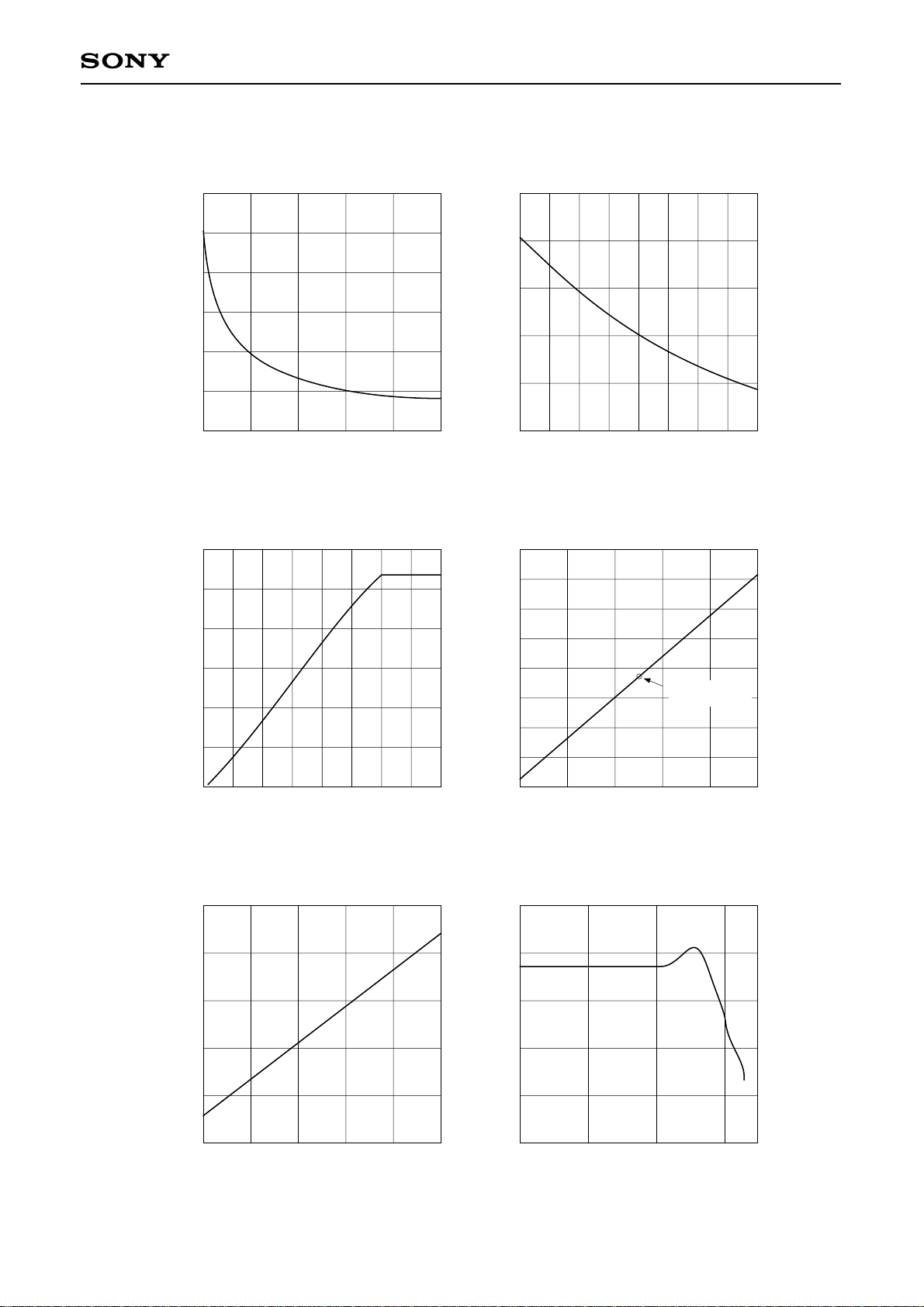
CXA2111R
3.0
2.5
2.0
1.5
Gain [times]
1.0
0.5
0
0
4.0
3.5
3.0
R/G/B amplifier gain
2
(I
C: Standard setting)
12345
Control pin voltage (Pins 27, 28 and 29) [V]
R/G/B output black limiter voltage
R/G/B amplifier gain I2C characteristics
(Control pins = open)
0.60
0.55
0.50
0.45
Gain [times]
0.40
0.35
08 18 28 38 3F10 20 30
00
2
C setting [HEX]
I
R/G/B input clamp voltage characteristics
3.0
2.8
2.6
2.4
2.5
2.0
Output voltage [V]
1.5
1.0
1.0 1.5 2.5 3.5 4.5 5.0
2.0 3.0 4.0
Pin 12 (BLKLIM) voltage [V]
Pin 6 (SIDOUT) output
4.0
3.5
3.0
2.5
Pin 6 voltage [V]
2.0
2.2
2.0
Clamp voltage [V]
1.8
1.6
1.4
0
(Gamma OFF, amplifier gain = min.)
–7
–8
–9
Gain [dB]
–10
–11
When Pin 25 =
open
145
23
Pin 25 (CLPLEV) voltage [V]
R/G/B frequency response
1.5
0
1 3452
Control voltage (Pin 9/11) [V]
–12
0.1
1 10 100
Frequency [MHz]
– 17 –
Page 18

Package Outline Unit: mm
CXA2111R
52PIN LQFP(PLASTIC)
40
52
+ 0.08
0.32 – 0.07
39
1
0.25
0.1 ± 0.1
12.0 ± 0.2
∗ 10.0 ± 0.1
0.13
M
(11.0)
27
13
0.6 ± 0.15
26
14
0.65
A
0.32 – 0.07
+ 0.08
(0.3)
+ 0.1
1.5 0
B
0.1
+ 0.04
0.145 – 0.025
(0.125)
0° to 10°
(0.5)
DETAIL
A
NOTE: Dimension “∗” does not include mold protrusion.
SONY CODE
EIAJ CODE
JEDEC CODE
LQFP-52P-L01
LQFP052-P-1010
DETAIL
B
PACKAGE STRUCTURE
PACKAGE MATERIAL
LEAD TREATMENT
LEAD MATERIAL
PACKAGE MASS
EPOXY RESIN
PALLADIUM PLATING
COPPER ALLOY
0.3g
– 18 –
 Loading...