

Page 1
Dolby∗B-C Type Noise Reduction System for Playback
Description
The CXA2502M is a bipolar IC incorporating stereo
Dolby B-C type noise reduction (NR) system for
playback.
Pins of this IC are compatible with those of the
Dolby B type NR ICs CXA1102M/ CXA1552M.
A reduction in the number of external parts and
small package have been achieved due to the fact
that the spectral skewing circuits are all on-chip and
this IC is intended for playback.
Features
• Few external parts
• Spectral skewing circuit are on-chip
• NR OFF/B/C and AUX/TAPE switches
• Small package (16-pin SOP)
• Low current consumption 12mA Typ.
• Built-in two channels
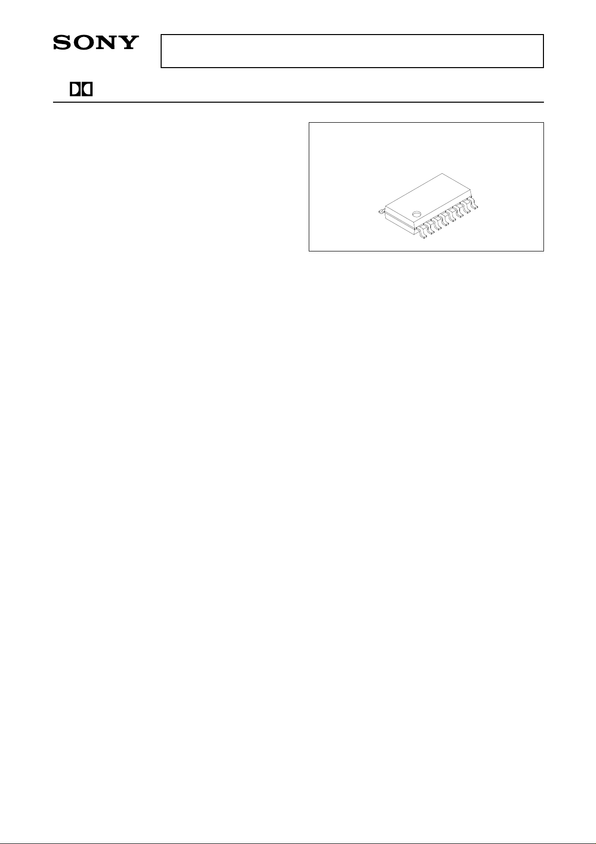
CXA2502M
16 pin SOP (Plastic)
Structure
Bipolar silicon monolithic IC
Absolute Maximum Ratings (Ta = 25°C)
• Supply voltage VCC 17 V
• Operating temperature Topr –40 to +85 °C
• Storage temperature Tstg –65 to +150 °C
• Allowable power dissipation
PD 600 (SOP) mW
∗
This IC is available only to the licensees of Dolby Laboratories Licensing Corporation from whom licensing and applications
information may be obtained.
∗
“Dolby” and the double D symbols are trademarks of Dolby Laboratories Licensing Corporation.
Sony reserves the right to change products and specifications without prior notice. This information does not convey any license by
any implication or otherwise under any patents or other right. Application circuits shown, if any, are typical examples illustrating the
operation of the devices. Sony cannot assume responsibility for any problems arising out of the use of these circuits.
– 1 –
E95621A5X-PS
Page 2
CXA2502M
(–6dBm)
LINEOUT1
P13
1µ
C13
C15
C14
TAPE AUXC12
68n
100n
9
TCL1
TCH1
10
LINEOUT1
11
MODE
12
LDET
HDET
LLS
HLS
CC
V
P1
SSK
Mode
Control
SSK
LLS
HLS
LDET
HDET
(–6dBm)
LINEOUT2
P23
8
TCL2
68n
C25
7
TCH2
C24
100n
6
5
LINEOUT2
NRSW
OFF
B
C
C23
1µ
P12
PBIN1
AUXIN1
(–30dBm)
R1
20k
1µ
1µ
C11
P11
(–30dBm)
IREF
13
PBIN1
1415
GND
AUXIN1
16
MOA
IREF
MOA
4
VCT
C1
47µ
3
PBIN2
Application circuits shown are typical examples illustrating the operation of the devices. Sony cannot assume responsibility for
1µ
C22
2
V
CC
C2
10µ
1
AUXIN2
1µ
C21
P21
PBIN2
AUXIN2
(–30dBm)
P22
(–30dBm)
any problems arising out of the use of these circuits or for any infringement of third party patent and other right due to same.
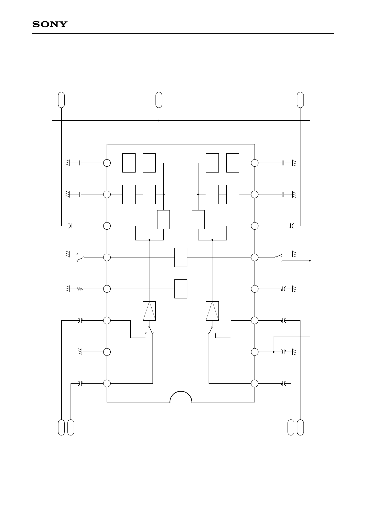
Block Diagram, Pin Configuration and Application Circuit
– 2 –
Page 3
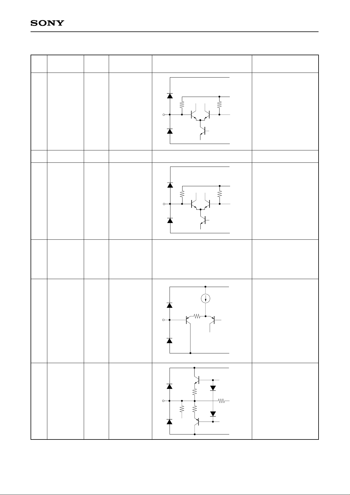
Pin Description
Pin
No.
1
16
2
3
14
Symbol Z (in) VDC (V) Equivalent circuit Description
AUX IN
VCC
PB IN
40K
40K
VCT
VCC
VCT
40k
40k
CXA2502M
VCC
VCT
Auxiliary input.
Reference level
= –30dBm
GND
Positive power supply.
VCC
VCT
Playback input.
Reference level
= –30dBm
4
5
6
11
VCT
NRSW
LINE OUT
—
GND
Dual power supply:
0
VCT
Ground
Single power supply:
Vcc/2
VCC
50µA
22k
—
NR control
High: C type
Medium:B type
Low: NR OFF
GND
VCC
200
0
VCT
200
Line output.
– 3 –
GND
Page 4
CXA2502M
Pin
No.
7
10
8
9
Symbol Z (in) VDC (V) Equivalent circuit Description
VCC
TCH
TCL
—
—
0.4V
0.4V
36k13k
330k
GND
VCC
13.5k
480k
GND
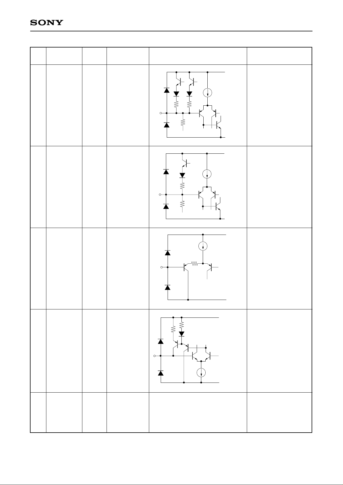
Time constant for the
HLS.
Time constant for the
LLS.
12
13
MODE
IREF
—
VCC
50µA
22k
—
MODE control
High: TAPE
Low: AUX
GND
VCC
Reference current
0
1.25V
1.25V
which determines the
built-in filter cut-off
frequency.
GND
15
GND
GND
Dual power supply:
Negative power supply
Single power supply:
Ground
– 4 –
Page 5
CXA2502M
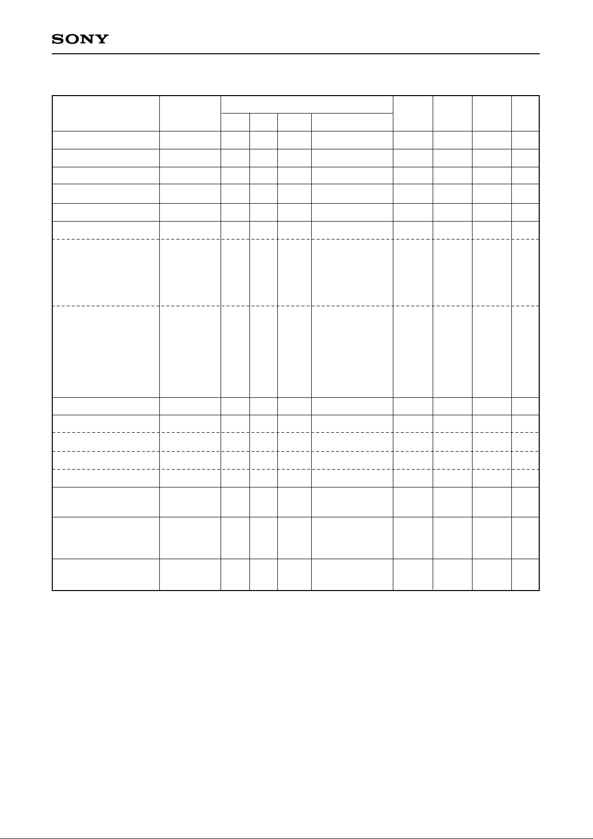
Electrical characteristics (Ta = 25°C, VCC = 9V)
∗
Min.
Typ.
Max.
Unit
Characteristics
Symbol
Measurement conditions
P/A
NR
f (Hz)
Other conditions
Operating voltage Vopr
Current consumption
LINEOUT level
AUX IN level
PB IN level
ICC
Vlout
Vlin
Vpin
Decode characteristics
B type boost
B-R-1
(1)
B-R-2
(2)
B-R-3
(3)
B-R-4
(4)
C type boost
C-R-1
(1)
C-R-2
(2)
C-R-3
(3)
C-R-4
(4)
C-R-5
(5)
C-R-6
(6)
Signal handling
Vomax PB OFF 1k THD = 1% 13.5 16.0 — dB
Total harmonic distortion
AUX
PB
PB
PB
PB
PB
PB
PB
PB
PB
PB
PB
OFF
OFF
OFF
B
B
B
B
C
C
C
C
C
C
1k
1k
1k
500
5k
10k
10k
500
500
2k
2k
5k
10k
No Signal
–25dB
–25dB
–40dB
0dB
–60dB
–25dB
–60dB
–25dB
–25dB
0dB
7.2
8.0
–7.0
–32
–32
1.4
3.9
9.7
–1.1
14.2
7.2
18.7
5.4
3.5
–5.5
—
12.0
–6.0
–30
–30
2.9
5.4
10.4
0.4
16.2
9.2
20.7
7.4
5.5
–3.5
16.0
18.0
–5.0
–28
–28
4.4
6.9
11.4
1.9
18.2
11.2
22.7
9.4
7.5
–1.5
V
mA
dBm
dBm
dBm
dB
dB
dB
dB
dB
dB
dB
dB
dB
dB
1) NR OFF
2) B
3) C
Decode
S/N ratio
REC-PB
PB-REC
ch to ch
Offset voltage
(OFF-C type)
∗
0dB means the level which provides –6dBm to the line output when NR is off.
THD (OFF)
THD (B)
PB OFF 1k +10dB — 0.01 0.1 %
PB B 1k +10dB — 0.03 0.1 %
THD (C) PB C 1k +10dB — 0.04 0.2 %
SN (CCIR)
CT-1
CT-2
CT-3
Voff
PB
PB
AUX
PB
PB
C—
OFF
OFF
OFF
OFF
→ C
1k
1k
1k
—
Rg = 5kΩ
(CCIR/ARM)
0dB
0dB
0dB
75 83 — dB
—
—
—
–100
–85
–85
–68
0 100
–70
–70
–60
dB
dB
dB
mV
– 5 –
Page 6
VCC
S3
Audio
Analyzer
CXA2502M
C13
1µ
S2_1
Meter
DC Volt
68n
C15
C14
100n
VMODE
R1
20K
1µ
C12
1µ
C11
9
10
11
12
13
14
15
16
TCL1
TCH1
MODE
IREF
PBIN1
GND
AUXIN1
A
LINEOUT1
CXA2502M
TCL2
8
TCH2
7
LINEOUT2
6
NRSW
5
VCT
4
PBIN2
3
V
CC
2
AUXIN2
1
C25
C24
C2
C22
C1
C21
68n
100n
100µ
1µ
100µ
1µ
S2_2
VNRSW
Filter
CCIR/ARM
1µ
C23
S12
S11
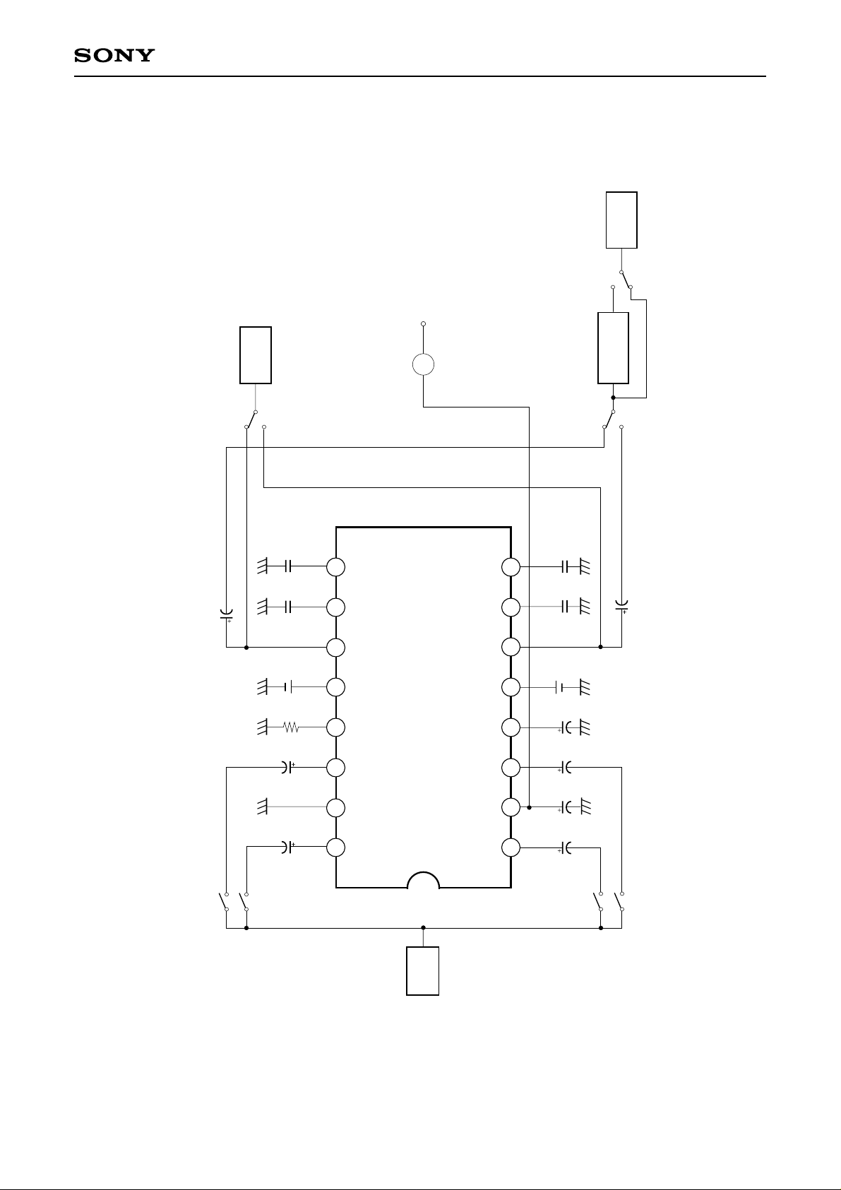
Electrical Characteristics Measurement Circuit
Audio
– 6 –
SG
S21
S22
Page 7
CXA2502M
Application Note
The CXA2502M is a stereo Dolby B-C type NR IC like the CXA1560 series.
Few external parts and smaller package can be achieved because this IC has a built-in spectral skewing circuit
and the reduced number of pins for playback.
1) Power Supply
The CXA2502M is designed to operate on either single or dual power supply.
For dual power supply, connect VCT pin to GND, and GND pin to the negative power supply.
For single power supply, connect GND pin to GND. VCC/2, generated from the internal circuit, is output to
VCT pin.
Connect a by-pass capacitor between this pin and GND.
The operating voltage range is 7.0 to 16V, which satisfies the signal handling of 12dB specified by the Dolby
Laboratories.
2) Operation Mode Control
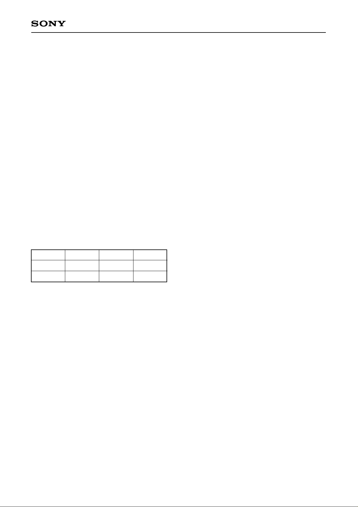
The CXA2502M has built-in electronic switches. The operations are controlled by the DC voltages of NRSW
and MODE control pins. Table 1 shows the switching truth tables.
For single power supply, VH, VM and VL correspond to VCC, VCC/2 and GND, respectivery.
For dual power supply, VH, VM and VL correspond to VCC, GND and VEE, respectively.
Refer to "threshold" on the characteristics graph for the thresholds of the control voltages. NRSW and MODE
control pins are connected to VCT via a 50kΩ resistor, so when the pin is open, VM condition results.
VH VM VL
NRSW C type B type NR OFF
MODE
→
TAPE AUX
Table 1
3) Reference level
The CXA2502M Dolby level is –6dBm (388mVrms). The reference level of the playback input pin (PB IN) is
defined as the levels which provide the line output level to the line output pin (LINE OUT) in NR OFF mode.
– 7 –
Page 8
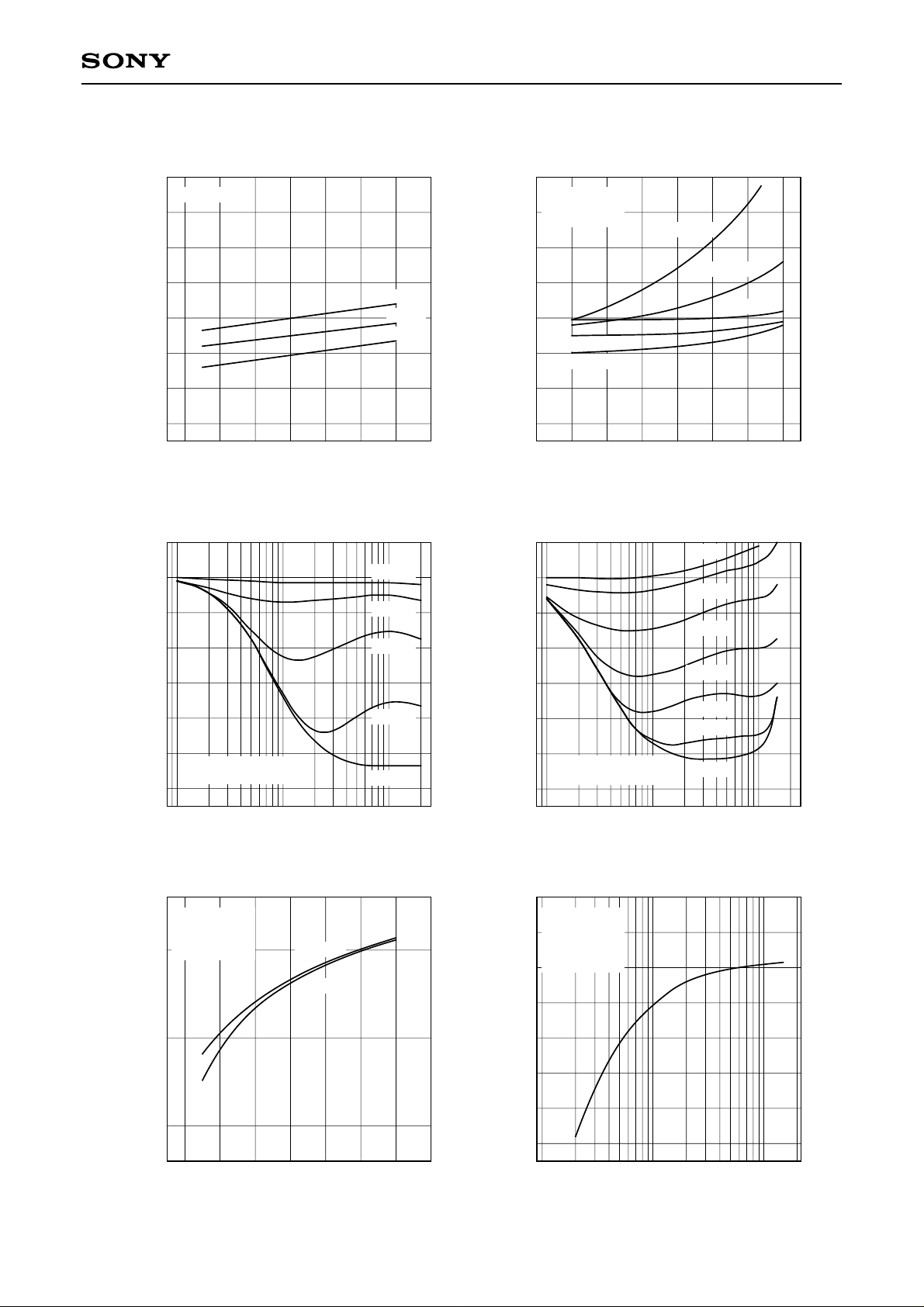
Example of Representative Characteristics
CXA2502M
Quiescent current consumption vs. Supply voltage
Decode Mode
15
14
13
12
11
10
– Quiescent current consumption [mA]
CC
I
9
4 6 8 10121416
VCC – Supply voltage [V]
NR OFF
B type
C type
B type decode characteristics
–2
0
2
4
6
8
Decode boost [dB]
0dB
–10dB
–20dB
–30dB
Quiescent current consumption vs. Input level
Decode Mode
VCC = 9V
15
0dB = –6dBm
14
13
12
B f = 1kHz
11
C f = 1kHz
10
– Quiescent current consumption [mA]
CC
I
9
–12 0 4 8 12
–8 –4
C f = 10kHz
B f = 10kHz
NR OFF
Input level [dB]
C type decode characteristics
–4
0
4
8
12
Decode boost [dB]
16
0dB
–10dB
–20dB
–30dB
–40dB
–50dB
10
VCC = 9V
0dB = Lineout Level
12
Decode Mode
f = 1kHz
THD = 1%
20
0dB = –6dBm
10
Signal handling [dB]
0
4 6 8 10121416
–40dB
500200100 1k 2k 5k 10k 20k
Frequency [Hz]
Signal handling
NR OFF
C type
VCC – Supply voltage [V]
20
VCC = 9V
0dB = Lineout Level
24
500200100 1k 2k 5k 10k 20k
Frequency [Hz]
Load characteristics
Decode Mode
VCC = 9V
12
THD = 1%
f = 1kHz
NR OFF
10
8
6
4
Maximum output level [dBm]
2
0
100 300 1k
Frequency [Hz]
–60dB
3k 10k
– 8 –
Page 9
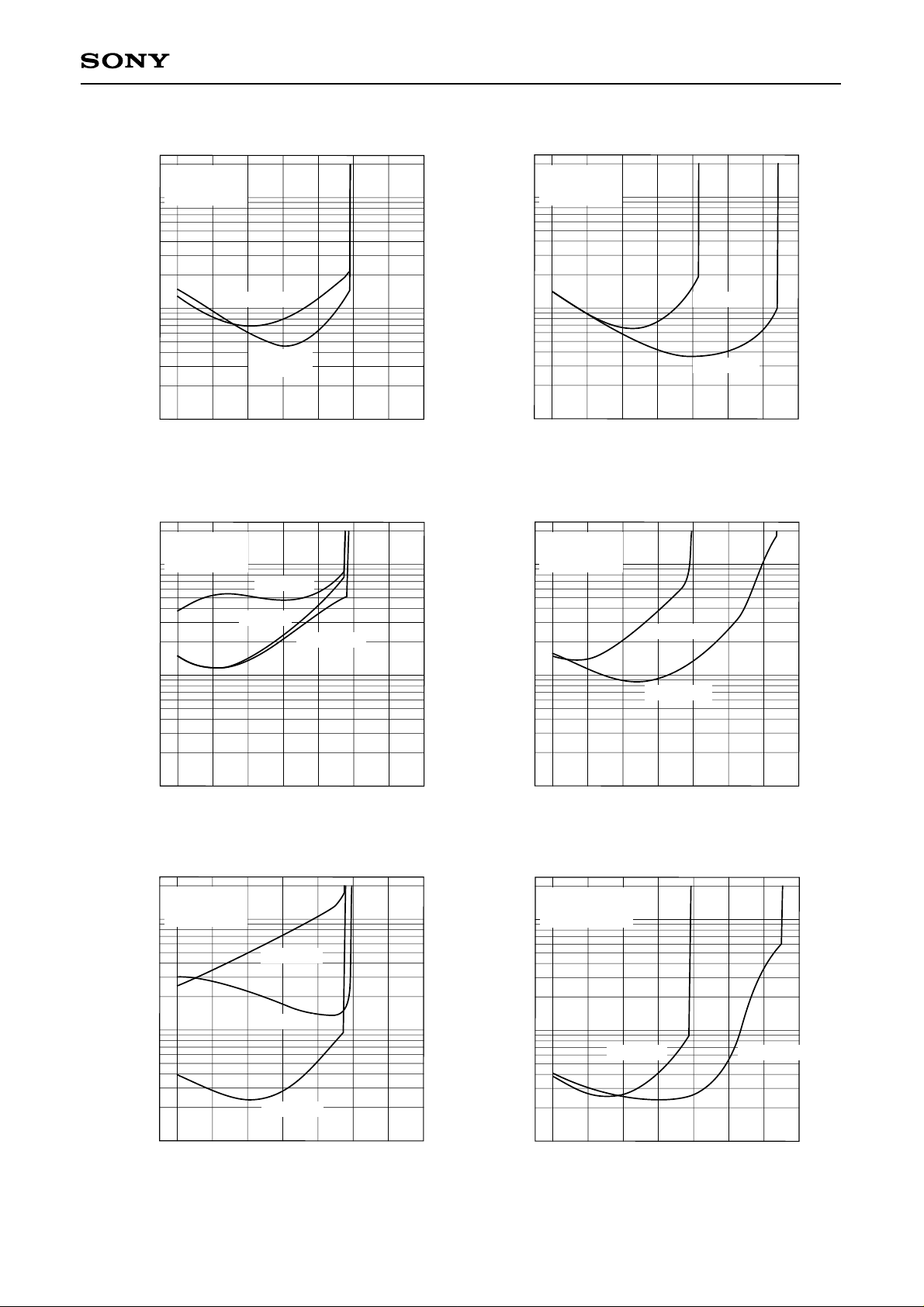
CXA2502M
Decode Mode
VCC = 9V
0.1
0dB = –6dBm
0.01
Distortion [%]
0.001
–4 0 4 8 12 16 20
Decode Mode
VCC = 9V
0.1
0dB = –6dBm
NR OFF total harmonic distortion-1
f = 10kHz
f = 100Hz
f = 1kHz
Output level [dB]
B type total harmonic distortion-1
f = 100Hz
Decode Mode
f = 1kHz
0.1
0dB = –6dBm
0.01
Distortion [%]
0.001
–4 0 4 8 12 16 20
Decode Mode
f = 1kHz
0.1
0dB = –6dBm
NR OFF total harmonic distortion-2
VCC = 7V
VCC = 16V
Output level [dB]
B type total harmonic distortion-2
0.01
Distortion [%]
0.001
Distortion [%]
–4 0 4 8 12 16 20
Decode Mode
VCC = 9V
0dB = –6dBm
1.0
0.1
f = 1kHz
f = 10kHz
Output level [dB]
C type total harmonic distortion-1
f = 10kHz
f = 100Hz
0.01
Distortion [%]
0.001
–4 0 4 8 12 16 20
Decode Mode
f = 1kHz
0dB = –6dBm
1.0
0.1
Distortion [%]
VCC = 7V
VCC = 16V
Output level [dB]
C type total harmonic distortion-2
VCC = 7V VCC = 16V
f = 1kHz
0.01
–4 0 4 8 12 16 20
Output level [dB]
– 9 –
0.01
–4 0 4 8 12 16 20
Output level [dB]
Page 10
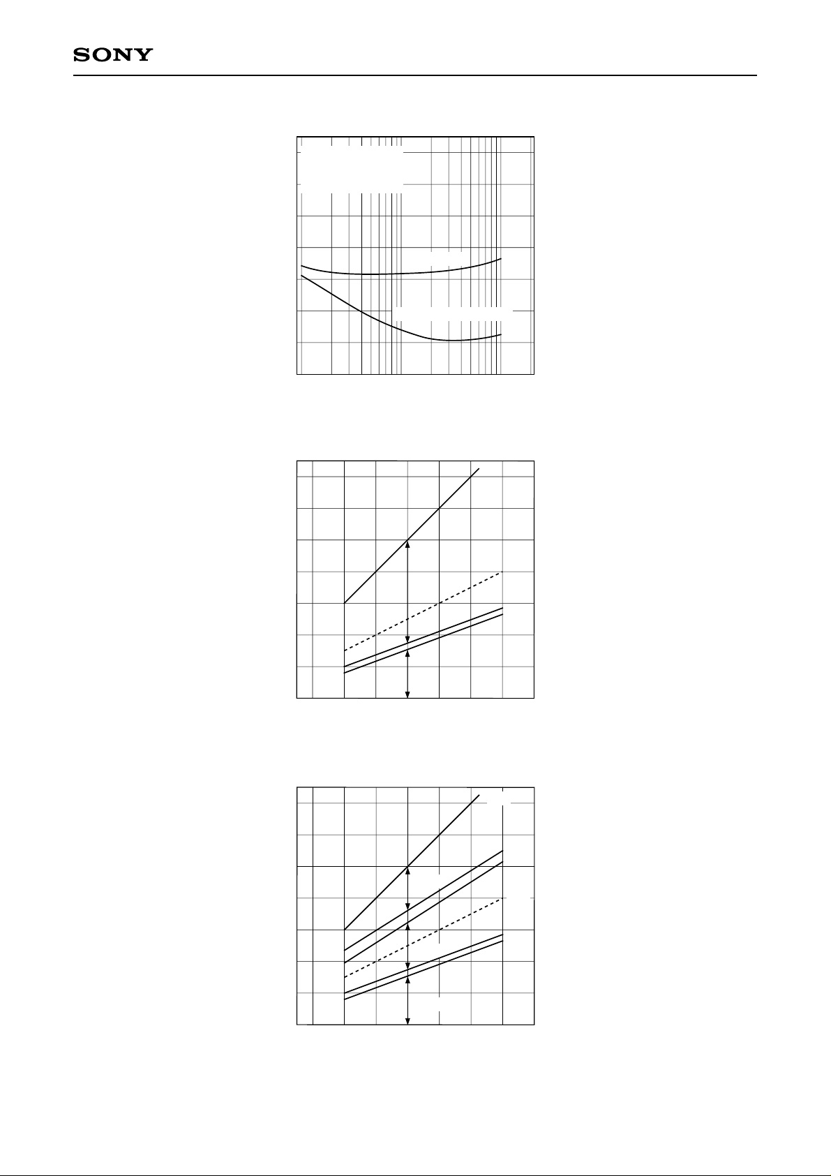
VCC = 9V
–30
Input = +10dB
Refer to Dolby Level
–40
NR OFF
–50
CXA2502M
Cross talk
–60
–70
Cross talk [dB]
–80
–90
100 300 1k
Frequency [Hz]
MODE control threshold
14
12
10
8
6
– MODE control voltage [V]
4
CM
V
2
0
4 6 8 10 12 14 16
VCC – Power supply [V]
CH to CH
AUX to PB, PB to AUX
3k 10k
PB
AUX
NR control threshold
14
12
10
8
6
– NR control voltage [V]
4
CN
V
2
0
4 6 8 10 12 14 16
VCC – Supply voltage [V]
VCC
C type
VCT
B type
NR OFF
– 10 –
Page 11
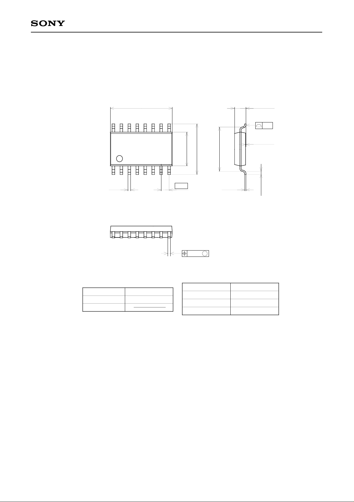
Package Outline Unit: mm
CXA2502M
16PIN SOP (PLASTIC)
+ 0.4
9.9 – 0.1
16
18
0.45 ± 0.1
9
+ 0.3
5.3 – 0.1
7.9 ± 0.4
1.27
M
0.24
6.9
0.2 – 0.05
+ 0.1
+ 0.4
1.85 – 0.15
0.15
+ 0.2
0.1 – 0.05
0.5 ± 0.2
SONY CODE
EIAJ CODE
JEDEC CODE
SOP-16P-L01
SOP016-P-0300
PACKAGE STRUCTURE
PACKAGE MATERIAL
LEAD TREATMENT
LEAD MATERIAL
PACKAGE MASS
EPOXY RESIN
SOLDER PLATING
COPPER ALLOY
0.2g
– 11 –
 Loading...