

Page 1
Low-voltage FM IF Amplifier
Description
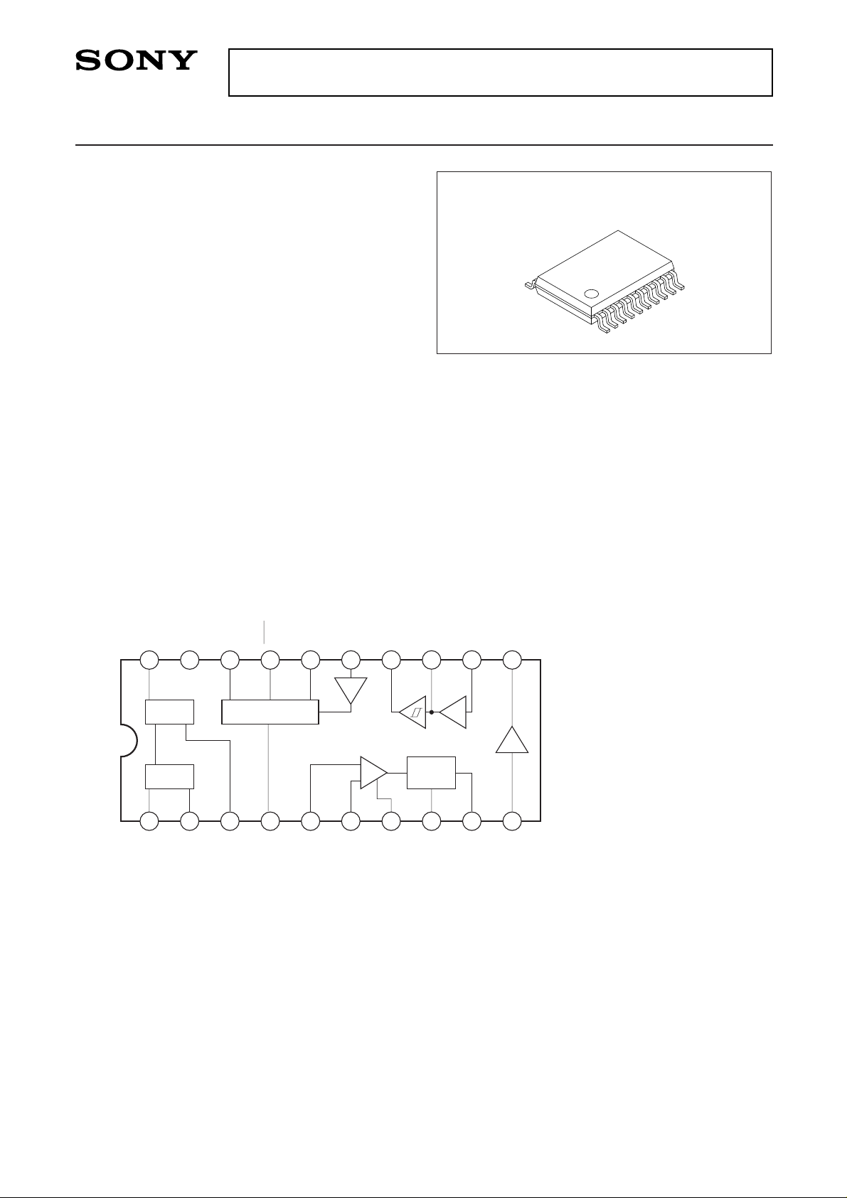
The CXA1884N is designed for FM communication
devices. They incorporate a paging system, mixer, IF
limiter, FM detector, operational amplifier, comparator,
and others.
Features
• Low operating voltage 1.0 to 4.0V
• Low power consumption 2mA at 1.5V
• Built-in power source voltage monitor
Applications
IF Amplifier for Paging System Receiver
Structure
Bipolar silicon monolithic IC
Block Diagram and Pin Configuration
Absolute Maximum Ratings (Ta = 25°C)
• Supply voltage Vcc 7 V
• Operating temperature Topr –20 to +75 °C
• Storage temperature Tstg –65 to +150 °C
Recommended Operating Conditions
Supply voltage Vcc 1.0 to 4.0 V
– 1 –
E97Z05A8Y
Sony reserves the right to change products and specifications without prior notice. This information does not convey any license by
any implication or otherwise under any patents or other right. Application circuits shown, if any, are typical examples illustrating the
operation of the devices. Sony cannot assume responsibility for any problems arising out of the use of these circuits.
CXA1884N
20 pin SSOP (Plastic)
RF IN
OSC1
GND
OSC2
LVA
MIX OUT
BSV
V
CC
VB OUT
IF IN
SENSE
IF P1
NRZ
IF P2
COMP IN
QD
A2 IN
DET OUT
A1 OUT
A1 IN
MIXER
OSC
QUAD
DET.
A2
ERR.
AMP
REG.
IF LIM.
A1
2
3
4
5
6
7
8
9
10
1
11
16
17
18
19
20
12
13
14
15
Note) DET. : DETECTOR
LIM. : LIMITER
REG. :REGURATOR
ERR. : ERROR CORRECTION
Page 2
– 2 –
CXA1884N
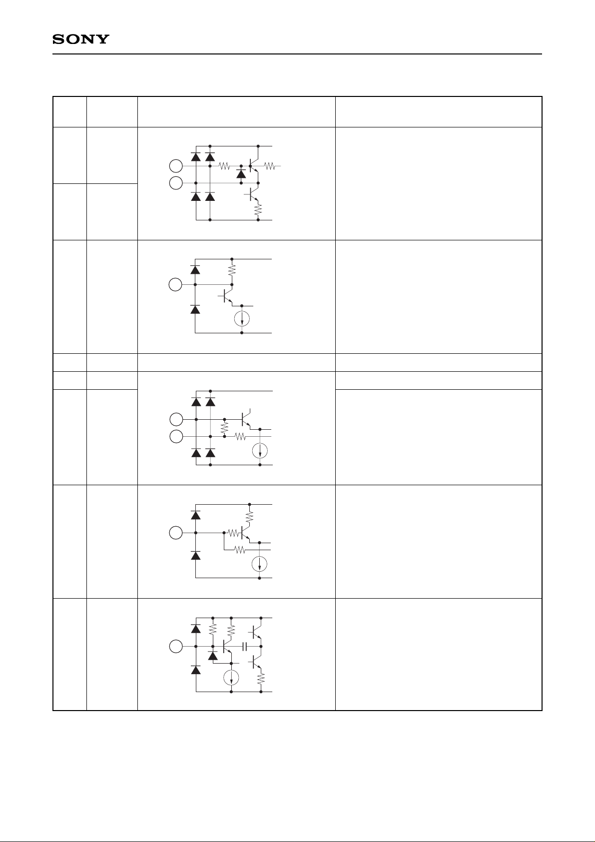
Pin Description
Pin
No.
1 OSC1
Those pins are connected to the external
parts of an oscillating circuit.
The oscillator is an internally-biased Colpitts
type with the collector, base, and emitter
connections at Vcc, pins 1 and 2
respectively.
Mixer output pin. Connect a 455kHz ceramic
filter between this pin and the IF IN pin.
Vcc pin.
Input pin for the IF limiter amplifier.
Connection pin of the bypass capacitor for
the IF limiter amplifier. Connect a capacitor of
about 0.047µF between this pin and ground
(or Vcc).
Connection pin of the bypass capacitor for
the IF limiter amplifier. Connect a capacitor of
about 0.047µF between this pin and ground
(or Vcc).
Connected to a quadrature detector phase
shifter.
OSC2
MIX OUT
VCC
IF IN
IF P1
IF P2
QD
2
3
4
5
6
7
8
Symbol Equivalent circuit Description
VCC
GND
2
1
VCC
GND
3
VCC
GND
5
6
VCC
GND
7
VCC
GND
8
Page 3
– 3 –
CXA1884N
Pin
No.
9
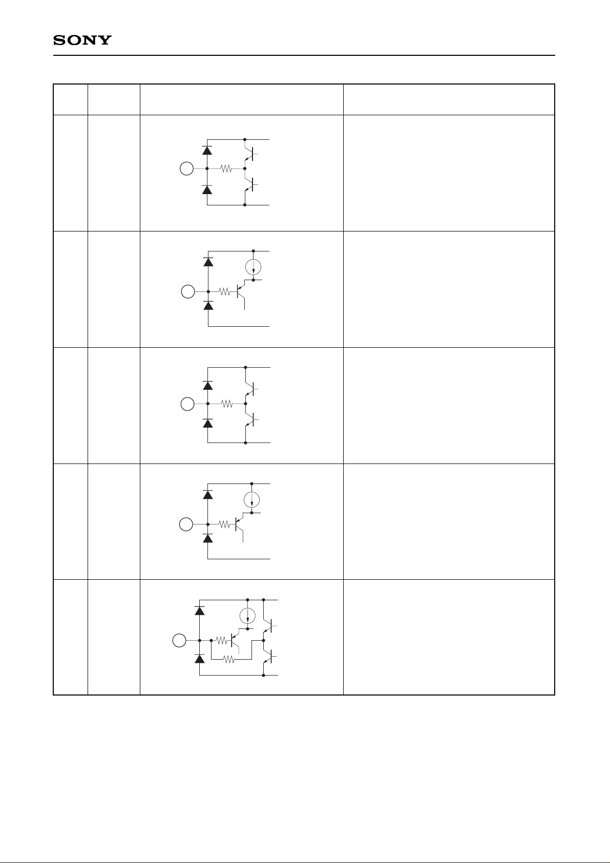
DET OUT
Recovered signal output.
Symbol Equivalent circuit Description
9
VCC
GND
10
A1 IN
Input pin of inverting OP amplifier A1.
VCC
GND
10
11
A1 OUT
Output pin of OP amplifier A1.
VCC
GND
11
12
A2 IN
Input pin of OP amplifier A2.
VCC
GND
12
13
COMP
IN
Input pin of the comparator.
This pin is internally connected to the output
of OP amplifier A2.
VCC
GND
13
Page 4

– 4 –
CXA1884N
Pin
No.
15
SENSE
Voltage control pin for external bias supply.
Symbol Equivalent circuit Description
VCC
GND
15
16
VB OUT
Supplies bias voltage to external circuit
transistors and others.
VCC
GND
16
20
RF IN
Mixer input pin.
20
VCC
GND
17
BSV
Reduces IC power consumption.
Lowering pin voltage beiow 0.35V stops IC
operation.
GND
17
18
LVA
Output pin for Low Voltage Alarm (LVA).
The pin turns to high impedance when
power voltage drops below 1.05V.
18
GND
19
GND
Ground pin.
14 NRZ
NRZ (Non Return Zero) output pin.
GND
14
Page 5
– 5 –
CXA1884N
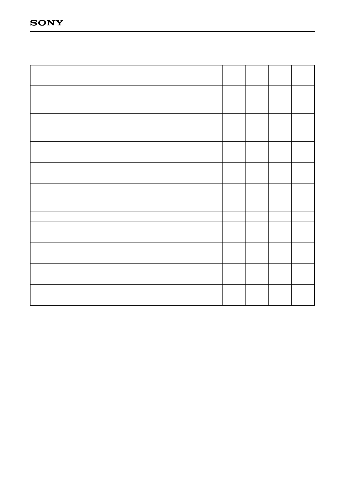
Electrical Characteristics
(VCC = 1.5V, Ta = 25°C, fs = 21.7MHz, fMOD = 256Hz, fDIV = 2.3kHz, AMMOD = 30%)
Item
Power consumption (during operation)
Power consumption
(during battery saving)
Input for –3dB Limiting
AM rejection ratio
OP amplifier input bias current
OP amplifier open loop gain
OP amplifier output voltage amplitude
Comparator hysteresis width
NRZ∗output leak current
NRZ∗saturation voltage
VB output current
VB output voltage
Sense voltage
LVA threshold voltage
LVA hysteresis width
LVA output leak current
LVA saturation voltage
Recovered signal voltage
BSV high level
BSV low level
ICC
ICCS
VIN (LIM)
AMRR
IBIAS
AV
VO
VTW
ILNRZ
VSATNRZ
IOUT
VBOUT
VSEN
VPML
VPMTH
ILLVA
VSATLVA
VDET
VTHBSV
VTLBSV
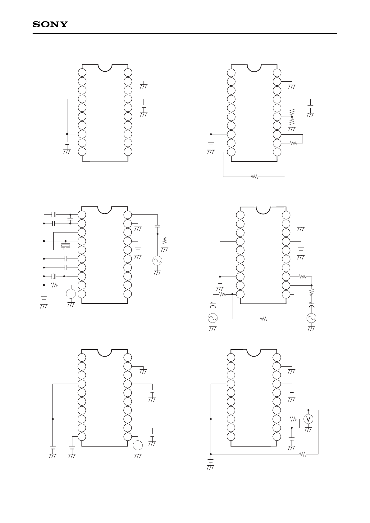
Test circuit 1
Test circuit 1
VI = 0.3V
Test circuit 3
VIN = 60dBµ
Test circuit 3
Test circuit 2
Test ciTcuit 4
Test circuit 5
Test circuit 6
Test circuit 7
ISINK = 200µA
Test circuit 8
VB = 0.9V
Test circuit 9
Test circuit 2
Test circuit 10
VPMH – VPML
Test circuit 7
Test circuit 8
Test circuit 3
1.2
—
—
25
—
45
0.25
30
—
—
0.1
0.95
85
1.00
35
—
—
10
0.95
—
2.0
—
7
—
30
60
—
40
—
—
—
—
100
1.05
50
—
—
—
—
—
2.6
20
—
—
100
—
—
50
5.0
0.4
—
—
115
1.10
70
5.0
0.4
—
—
0.35
mA
µA
dBµ
dB
nA
dB
Vp-p
mV
µA
V
mA
V
mV
V
mV
µA
V
mVrms
V
V
Symbol Condition Min. Typ. Max. Unit
∗
NRZ: Non Return Zero
Page 6
– 6 –
CXA1884N
Electrical Characteristics Test Circuit
VI
0.95V
VCC
1.5V
2
3
4
5
6
7
8
9
10
11
12
13
14
15
16
17
18
19
20
1
VI
0.95V
VCC
1.5V
7.5k
1k
RNF1
100k
RNF2
100k
2
3
4
5
6
7
8
9
10
11
12
13
14
15
16
17
18
19
20
1
VI
0.95V
VCC
1.5V
C IN 1
100p
RL
50
V IN 1
21.7MHz
Vo
CP2
0.047µ
CP1 0.047µ
CF1 455k
15p
22p
4.7k
2
3
4
5
6
7
8
9
10
11
12
13
14
15
16
17
18
19
20
1
VI
0.95V
VCC
1.5V
RNF1
10k
RNF2
10k
R IN 1
10k
V IN 1
0.1Vp-p
C IN 1
10µ
V IN 2
0.1Vp-p
C IN 2
10µ
RNF2
10k
2
3
4
5
6
7
8
9
10
11
12
13
14
15
16
17
18
19
20
1
VI
0.95V
VCC
1.5V
V IN2
0.1V
V
IN1
7V
2
3
4
5
6
7
8
9
10
11
12
13
14
15
16
17
18
19
20
1
Vo
VI
0.95V
VCC
1.5V
RL
10k
2
3
4
5
6
7
8
9
10
11
12
13
14
15
16
17
18
19
20
1
V IN
0.2 to 0.3V
RNF 10k
CP (C)
Test circuit 2Test circuit 1
Test circuit 4Test circuit 3
Test circuit 6
Test circuit 5
Page 7
– 7 –
CXA1884N
VCC
1.5V
VI
0.95V
VCC
1.5V
2
3
4
5
6
7
8
9
10
11
12
13
14
15
16
17
18
19
20
1
VI
0.95V
VCC
1.5V
VI
0.3V
RNF 10k
IS2
200µA
IS1
200µA
2
3
4
5
6
7
8
9
10
11
12
13
14
15
16
17
18
19
20
1
VCC
1.5V
VI
0.95V
VS
0.15V
IS
200µA
2
3
4
5
6
7
8
9
10
11
12
13
14
15
16
17
18
19
20
1
VI
0.95V
VCC
1.5V
CP
(C)
2
3
4
5
6
7
8
9
10
11
12
13
14
15
16
17
18
19
20
1
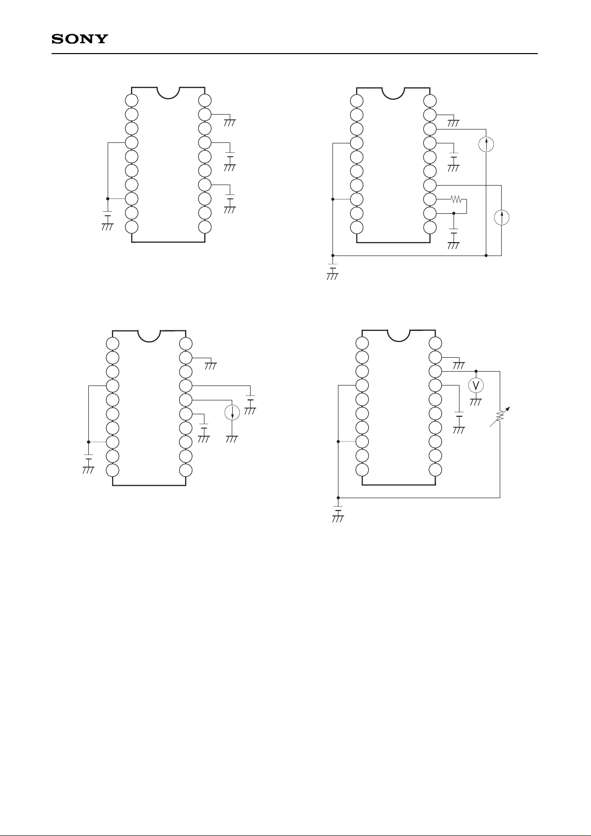
Test circuit 8Test circuit 7
Test circuit 10Test circuit 9
Page 8

– 8 –
CXA1884N
Test Method
Input for –3dB Limiting VIN (LIM)
Use test circuit 3. Apply a signal with the following characteristics to SIG IN.
Signal frequency: fs = 21.7MHz Modulation frequency: fMOD = 256Hz
Frequency deviation: fDIV = 2.3kHz Signal level: VL = 40dBµ
Here, the value of VAC is specified as VAC1. Next, the signal level VL is changed to 19dBµ and VAC value is
hence specified as VAC2.
20 log < 3dB
AM rejection ratio (AMRR)
Use test circuit 3. Apply a signal with the following characteristics to SIG IN.
Signal frequency: fs = 21.7MHz Modulation frequency: fMOD = 256Hz
Frequency deviation: fDIV = 2.3kHz Signal level: VL = 40dBµ
Here, the value of VAC is specified as VAC1. Next, AM is modified to:
Modulation ratio: AMMOD = 30% Modulation frequency: fMOD = 256Hz
and the VAC value is hence specified as VAC2.
AMRR = 20 log > 25dB
Recovered signal voltage VDET
Use test circuit 3. Apply a signal with the following characteristics to SIG IN.
Signal frequency: fs = 21.7MHz Modulation frequency: fMOD = 256Hz
Frequency deviation: fDIV = 2.3kHz Signal level: VL = 50dBµ
Here, the value of the Pin 9 output voltage is expressed as VDET.
OP amplifier output voltage amplitude VO
Use test circuit 5. If output voltage V is expressed as V1 when VIN is 0.1V, and as V2 when VIN is 0.3V, it
follows that:
VO = V1 – V2
Comparator hysteresis width VTW
Use test circuit 6. Vary VIN between 0.1 to 0.3V.
Specify VIN voltage, as V1 when (C) voltage changes from low to high.
Similarly, specify VIN voltage as V2, when (C) voltage changes from high to low.
Therefore: VHY VTW = V1 – V2
LVA threshold voltage VPML and recovery voltage VPMH
Use test circuit 10. Vary power voltage Vcc from 1.3 to 0.95V.
Specify Vcc as VPML, when (C) voltage changes from low to high.
Similarly, specify Vcc as VPMH, when (C) voltage changes from high to low.
VAC1
VAC2
VAC1
VAC2
Page 9

– 9 –
CXA1884N
Design Reference Values (Ta = 25°C, Vcc = 1.4V)
Item
Mixer input resistance
Mixer input capacity
Mixer output resistance
IF input resistance
IF gain stability
Detector output resistance
OP amplifier max. input voltage
OP amplifier min. input voltage
Comparator max. input voltage
Comparator min. input voltage
OP amplifier off-set voltage
RIN (MIX)
CIN (MIX)
ROUT (MIX)
RIN (IF)
GN (IF)
ROUT (QD)
VINMAX
VINMIN
VINMAXCOMP
VINMINCOMP
VOFS
Ta = –20 to +60°C
1.3
—
1.44
1.44
—
1.28
—
0.05
—
0.05
—
1.6
4.0
1.8
1.8
±6
1.6
—
—
—
—
—
1.9
—
2.16
2.16
—
2.0
0.39
—
0.39
—
3
Symbol Condition Min. Typ. Max.
kΩ
pF
kΩ
kΩ
dB
kΩ
V
V
V
V
mV
Unit
Application Circuit
MIXER
OSC
DET
ERR
REG
LIM
15p
22p
20.945MHz
0.047µ 0.047µ
4.7k
1µ
4.7µ
(BP)
or 1µ
C1
C2
R3
R2
C3
R4
R6
C4
R5
56k
68k0.1µ
6.8k
27k
BATT.S
DATA
AUDIO
LVA
V
CC
TO RF AMP TO 1ST MIX TO 2nd MIX
A2
A1
2
3
4
5
6
7
8
9
10
1
11
16
17
18
19
20
12
13
14
15
CFVM455
CDB455C3
R1
Application circuits shown are typical examples illustrating the operation of the devices. Sony cannot assume responsibility for
any problems arising out of the use of these circuits or for any infringement of third party patent and other right due to same.
Page 10

– 10 –
CXA1884N
VCC
Ceramic filter
2
3
1
(a)
Ceramic filter
2
3
1
From LOCAL SIG
(b)
Fig. 1
3) Mixer
This IC's mixer is of the double balance type. Pin 24 is the input pin. Input through a suitable alignment circuit.
Input impedance is at 1.6kΩ. The mixer output features a built-in 1.6kΩ Ioad resistance at Pin 3.
4) IF filter
The filter to be connected between this IC's mixer and the IF limiter should have the following specifications.
I/O impedance: 1.6kΩ ± 10%
Band width: Use according to application
1) Supply
This IC incorporates a regulation and is designed to operate steadily on a wide range of supply voltage from
1.0 to 4.0V.
Decoupling on the wiring to the supply pin (Pin 4) should be done as close to the pin as possible.
2) Oscillation input
Oscillation input method
(a) Using Pins 1 and 2, input self-excited oscillation signals through the composition of a Colpitts type crystal
oscillating circuit.
(b) Input local oscillation signals to Pin 1 directly.
Page 11

– 11 –
CXA1884N
VCC
Coil
7
8
9
DET OUTPUT
Fig. 3
VCC
7
8
9
DET OUTPUT
Ceramic
discriminator
CDB 455 C3
4.7k
(a) Coil (b) Ceramic discriminator
5) IF limiter
The IF limiter of this IC features a gain of about 100dB. To this effect, the following points should be
considered for the wiring connecting IF limiter input pin (Pin 5) and decoupling capacitor pins (Pins 6 and 7).
(a) Wiring to mixer output (Pin 3) and IF limiter input (Pin 5) should be as short and as far apart as possible
to avoid neutral interference.
(b) Connect a decoupling capacitor to IF limiter IF P1 (Pin 6) and IF P2 (Pin 7).
Here the decoupling capacitor should be positioned as close as possible to each pin and the wiring be as
short as can be.
(c) As IF limiter output shows at QD (Pin 8), keep the wiring connected to QD pin R, L, C and the ceramic
discriminator as short as possible. Interference to the mixer output, IF limiter input and others must be
kept to a minimum.
VCC
3
4
5
6
7
8
Wiring as short and as far apart as possible As short as possible
Fig. 2
6) Detector
The detector is of the quadrature type. To phase shift, either R, L, C resonance circuit or the ceramic
discriminator is connected to Pin 8.
The phase capacitor of the quadrature detector is built-in. FM (FSK) signals demodulated by this detector have
their high frequency components dropped by the LPF formed inside from CRs, to be output at DET OUT (Pin 9).
DET OUT output impedance is about 3kΩ.
For the CXA1884N ceramic discriminator, CDB 455 C3 (Murata Production) is recommended.
Page 12
– 12 –
CXA1884N
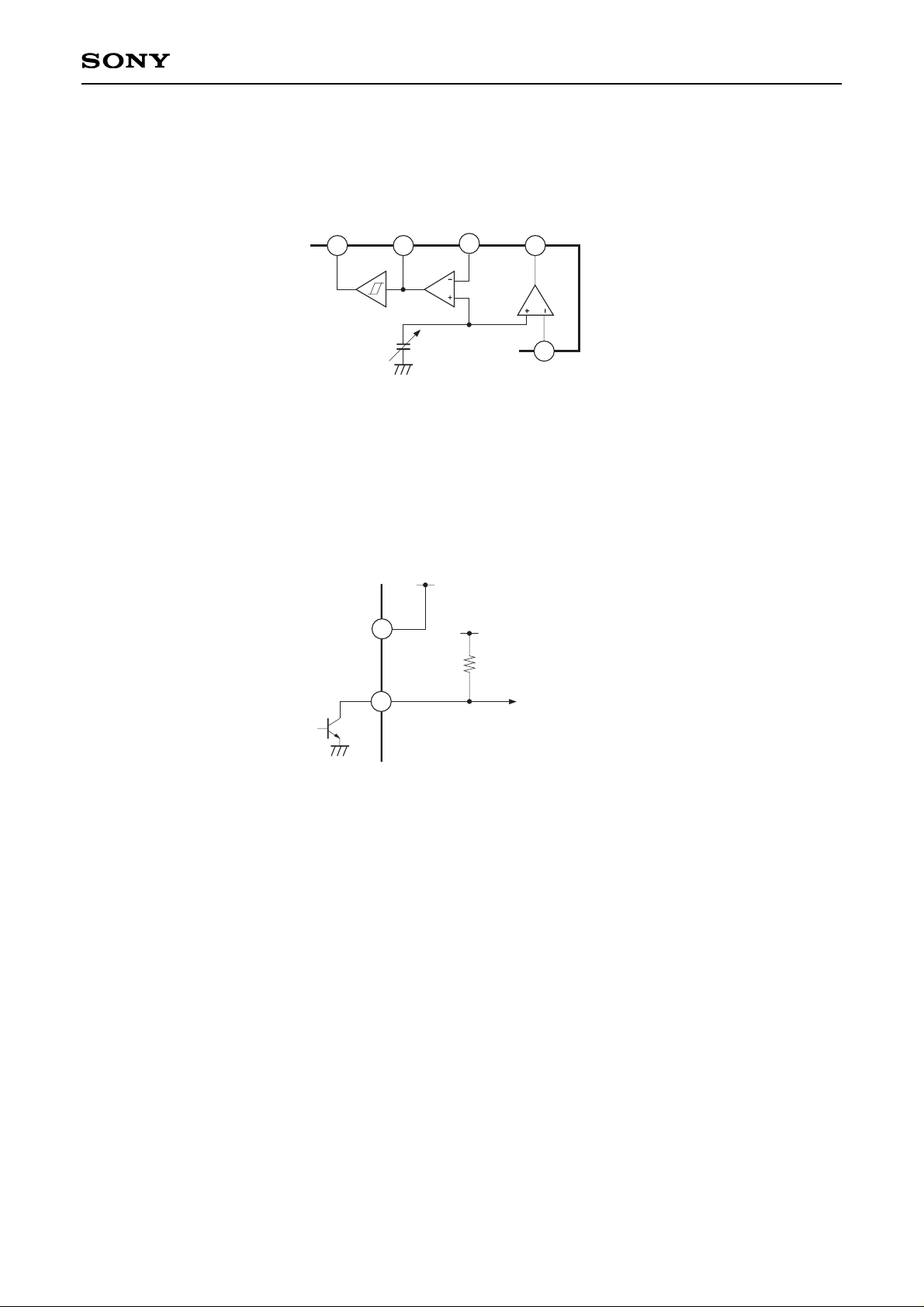
7) OP AMP, NRZ OUT
This IC has 2 built-in operation amplifiers.
One of these operation amplifiers is connected inside the IC to NRZ comparator.
10
0.2V
11
12
13
14
Fig. 4
Making use of these operation amplifiers an LPF or the sort is made up to eliminate noise during signal
demodulation and input to the following NRZ comparator.
NRZ comparator molds the waveform of input signals to output them as square waves. NRZ comparator output
is an open collector.
Accordingly as CPU is a CMOS, in case the supply voltage differs, by following the method indicated in Fig. 5
direct interfacing becomes possible.
CMOS IC
4
14
VCC for CMOS IC
V
CC 1.5V
V
CC
NRZ
OUT
Fig. 5
8) VB SENSE, VB OUT
This controls the base bias of the external transistor. Pin 16 VB OUT can be used as the previous amplifier 1st
mixer bias.
9) LVA OUT
When supply voltage turns low this pin turns to High (Open). Output is an open collector, and similarly as NRX
OUT, can directly drive CMOS.
This LVA setting voltage is at 1.05V ± 50mV with hysterisis versus supply voltage.
Hysterisis width is at 50mV ± 10mV.
Page 13

10) BSV
By turning this pin to low, this IC's operation can be stopped.
This pin can also be directly connected to CMOS.
Consumption current with BSV is 20µA (at 1.5V) and below.
– 13 –
CXA1884N
BSV
17
Fig. 6
Page 14

– 14 –
CXA1884N
–120 –110 –100 –90 –80 –70 –60 –50 –40 –30 –20 –10 0
–60
–50
–40
–30
–20
–10
0
Mixer input signal level [dBm]
Output characteristics [dB]
Mixer input signal vs. Output characteristics Input sensitivity
S + D + N
D + N
S + D + N
N
VCC = 1.5V, fMOD = 1kHz
fDEV = ±3kHz, fS = 21.7MHz
fC = 1.5kHz, K = L67
(–3dB)
4. Length Butterworth Cascade MFB (G = 4)
1000p
1.8µH
MIX
20
9
68k
33k
33k 470p
24k
22k
12k
0.01µ
2200p
200mV
200mV
13
1µ
0.01µ
A1
A2
4th LP Butterworth cascade MFB constant using OP1 and OP2 inside CXA1884N
9
R2
R3R1
C1
C2
R5
R6R4
C3
C4
200mV
200mV
13
A2
A1
fMOD
fc (–3dB)
A1 Gain
A2 Gain
R1
R2
R3
R4
R5
R6
C1
C2
C3
C4
256Hz
400Hz
1
4
47kΩ
47kΩ
22kΩ
47kΩ
180kΩ
33kΩ
0.012µF
680pF
0.015µF
1200pF
Page 15

– 15 –
CXA1884N
Supply voltage vs. Consumption current
1.0 2.0 3.0 4.0
V
CC – Supply voltage [V]
2.0
3.0
4.0
I
CC –
Consumption current [mA]
Input frequency vs. Conversion gain
1M 10M 100M
Input frequency [Hz]
–10
0
10
Conversion gain [dB]
LOCAL INPUT LEVEL = –10dBm
Logical input level vs. Mixer conversion
–40 –20 0 20
Logical input level [dBm]
10
20
Mixer conversion level [dB]
–10
0
–20
–30
–30 –10 10
Test the
ratio
between A
and B.
A
B
OSC IN
RF IN
f = 21.245MHz
Page 16
– 16 –
CXA1884N
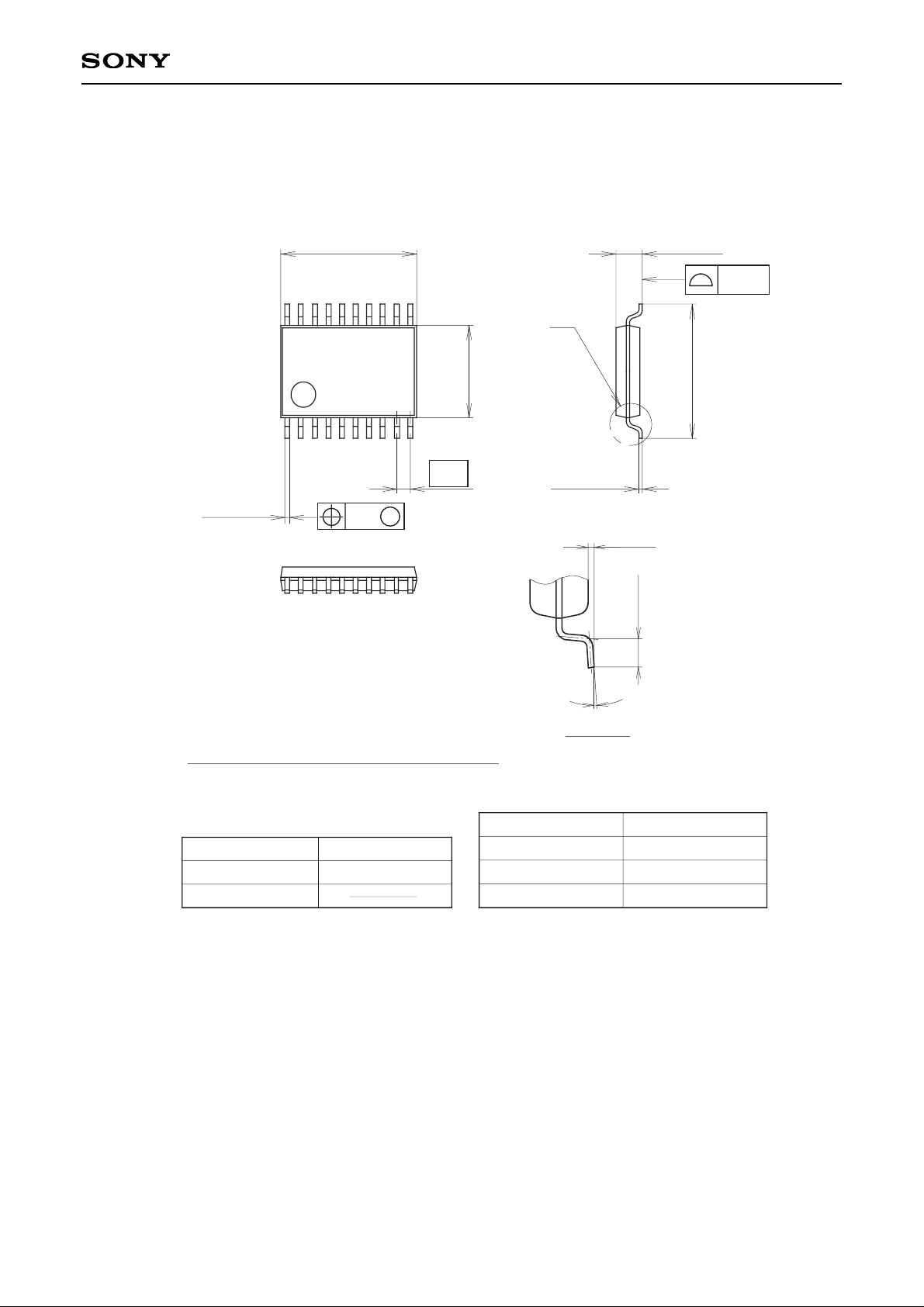
Package Outline Unit: mm
20PIN SSOP (PLASTIC)
SONY CODE
EIAJ CODE
JEDEC CODE
PACKAGE STRUCTURE
PACKAGE MATERIAL
LEAD TREATMENT
LEAD MATERIAL
PACKAGE MASS
EPOXY RESIN
SOLDER / PALLADIUM
42/COPPER ALLOY
0.1g
SSOP-20P-L01
SSOP020-P-0044
0.1 ± 0.1
0.5 ± 0.2
0° to 10°
DETAIL A
PLATING
∗6.5 ± 0.1
∗4.4 ± 0.1
0.22 – 0.05
+ 0.1
0.65
20
11
10
1
A
0.1
+ 0.05
1.25 – 0.1
+ 0.2
0.15 – 0.02
6.4 ± 0.2
NOTE: Dimension “∗” does not include mold protrusion.
0.13
M
NOTE : PALLADIUM PLATING
This product uses S-PdPPF (Sony Spec.-Palladium Pre-Plated Lead Frame).
 Loading...