


MJ11028
© Semiconductor Components Industries, LLC, 2008
September, 2008 − Rev. 6
1 Publication Order Number:
MJ11028/D
MJ11028, MJ11030,
MJ11032 (NPN)
MJ11029, MJ11033 (PNP)
High-Current
Complementary Silicon
Power Transistors
High−Current Complementary Silicon Power Transistors are for use
as output devices in complementary general purpose amplifier
applications.
Features
• High DC Current Gain − h
FE
= 1000 (Min) @ I
C
= 25 Adc
h
FE
= 400 (Min) @ I
C
= 50 Adc
• Curves to 100 A (Pulsed)
• Diode Protection to Rated I
C
• Monolithic Construction with Built−In Base−Emitter Shunt Resistor
• Junction Temperature to + 200_C
• Pb−Free Packages are Available*
MAXIMUM RATINGS (T
J
= 25°C unless otherwise noted)
Rating
Symbol Value Unit
Collector−Emitter Voltage MJ11028/29
MJ11030
MJ11032/33
V
CEO
60
90
120
Vdc
Collector−Base Voltage MJ11028/29
MJ11030
MJ11032/33
V
CBO
60
90
120
Vdc
Emitter−Base Voltage V
EBO
5.0 Vdc
Collector Current − Continuous
− Peak (Note 1)
I
C
50
100
Adc
Base Current − Continuous I
B
2.0 Adc
Total Power Dissipation @ T
C
= 25°C
Derate Above 25°C @ T
C
= 100_C
P
D
300
1.71
W
W/°C
Operating and Storage Junction
Temperature Range
T
J
, T
stg
− 55 to +200
°C
THERMAL CHARACTERISTICS
Characteristic Symbol Max Unit
Maximum Lead Temperature for
Soldering Purposes for v 10 seconds
T
L
275
_C
Thermal Resistance, Junction−to−Case
R
q
JC
0.58 °C/W
Maximum ratings are those values beyond which device damage can occur.
Maximum ratings applied to the device are individual stress limit values (not
normal operating conditions) and are not valid simultaneously. If these limits are
exceeded, device functional operation is not implied, damage may occur and
reliability may be affected.
1. Pulse Test: Pulse Width = 5 ms, Duty Cycle ≤ 10%.
*For additional information on our Pb−Free strategy and soldering details, please
download the ON Semiconductor Soldering and Mounting Techniques
Reference Manual, SOLDERRM/D.
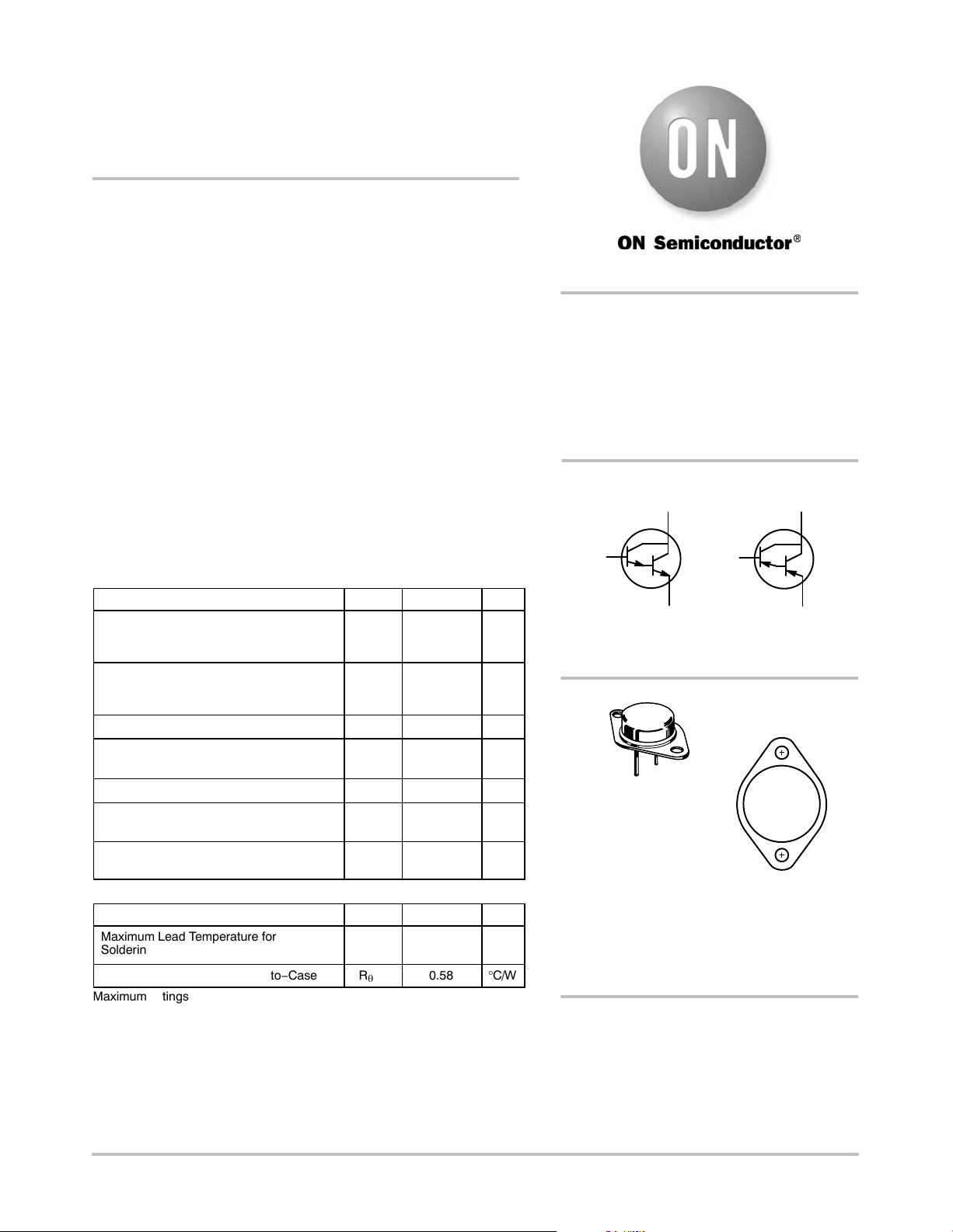
TO−204 (TO−3)
CASE 197A
STYLE 1
50 AMPERE
COMPLEMENTARY
DARLINGTON POWER
TRANSISTORS
60 − 120 VOLTS
300 WATTS
MARKING
DIAGRAM
MJ110xx = Device Code
xx = 28, 29, 30, 32, 33
G= Pb−Free Package
A = Location Code
YY = Year
WW = Work Week
MEX = Country of Orgin
http://onsemi.com
MJ110xxG
AYYWW
MEX
See detailed ordering and shipping information in the package
dimensions section on page 3 of this data sheet.
ORDERING INFORMATION
COLLECTOR
CASE
BASE
1
EMITTER 2
COLLECTOR
CASE
BASE
1
EMITTER 2
NPN PNP
MJ11028 MJ11029
MJ11030
MJ11032
MJ11033
2
1
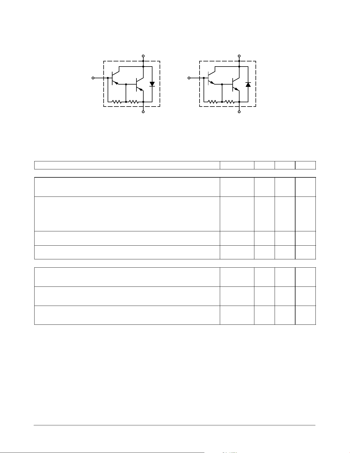
MJ11028, MJ11030, MJ11032 (NPN)
http://onsemi.com
2
Figure 1. Darlington Circuit Schematic
BASE
EMITTER
COLLECTOR
≈ 3.0 k ≈ 25
PNP
MJ11029
MJ11033
BASE
EMITTER
COLLECTOR
≈ 3.0 k ≈ 25
NPN
MJ11028
MJ11030
MJ11032
ELECTRICAL CHARACTERISTICS (T
C
= 25_C unless otherwise noted)
Characteristic
Symbol Min Max Unit
OFF CHARACTERISTICS
Collector−Emitter Breakdown Voltage (Note 1) MJ11028, MJ11029
(I
C
= 1 00 mAdc, I
B
= 0) MJ11030
MJ11032, MJ11033
V
(BR)CEO
60
90
120
−
−
−
Vdc
Collector−Emitter Leakage Current
(V
CE
= 60 Vdc, R
BE
= 1 kW) MJ11028, MJ11029
(V
CE
= 90 Vdc, R
BE
= 1 kW) MJ11030
(V
CE
= 120 Vdc, R
BE
= 1 kW) MJ11032, MJ11033
(V
CE
= 60 Vdc, R
BE
= 1 kW, T
C
= 150_C) MJ11028, MJ11029
(V
CE
= 120 Vdc, R
BE
= 1 kW, T
C
= 150_C) MJ11032, MJ11033
I
CER
−
−
−
−
−
2
2
2
10
10
mAdc
Emitter Cutoff Current
(V
BE
= 5 Vdc, I
C
= 0)
I
EBO
− 5
mAdc
Collector−Emitter Leakage Current
(V
CE
= 50 Vdc, I
B
= 0)
I
CEO
− 2
mAdc
ON CHARACTERISTICS (Note 1)
DC Current Gain
(I
C
= 25 Adc, V
CE
= 5 Vdc)
(I
C
= 50 Adc, V
CE
= 5 Vdc)
h
FE
1 k
400
18 k
−
−
Collector−Emitter Saturation Voltage
(I
C
= 25 Adc, I
B
= 250 mAdc)
(I
C
= 50 Adc, I
B
= 500 mAdc)
V
CE(sat)
−
−
2.5
3.5
Vdc
Base−Emitter Saturation Voltage
(I
C
= 25 Adc, I
B
= 200 mAdc)
(I
C
= 50 Adc, I
B
= 300 mAdc)
V
BE(sat)
−
−
3.0
4.5
Vdc
1. Pulse Test: Pulse Width v 300 ms, Duty Cycle v 2.0%.
 Loading...