


MJ11012
MJ11015 (PNP); MJ11012,
MJ11016 (NPN)
MJ11016 is a Preferred Device
High-Current
Complementary Silicon
Transistors
. . . for use as output devices in complementary general purpose
amplifier applications.
• High DC Current Gain −
h
= 1000 (Min) @ IC − 20 Adc
FE
• Monolithic Construction with Built−in Base Emitter Shunt
Resistor
• Junction Temperature to + 200_C
MAXIMUM RATINGS
Rating Symbol Value Unit
Collector−Emitter Voltage
Collector−Base Voltage
Emitter−Base Voltage V
Collector Current I
Base Current I
Total Device Dissipation @ TC = 25°C
Derate above 25°C @ T
Operating Storage Junction
Temperature Range
MJ11012
MJ11015/6
MJ11012
MJ11015/6
= 100°C
C
THERMAL CHARACTERISTICS
Characteristic Symbol Max Unit
Thermal Resistance, Junction−to−Case
Maximum Lead Temperature for Soldering Purposes for ≤ 10 Seconds
Stresses exceeding Maximum Ratings may damage the device. Maximum
Ratings are stress ratings only. Functional operation above the Recommended
Operating Conditions is not implied. Extended exposure to stresses above the
Recommended Operating Conditions may affect device reliability.
V
CEO
V
P
TJ, T
R
T
CB
EB
C
B
D
−55 to + 200 °C
stg
q
JC
L
60
120
60
120
5 Vdc
30 Adc
1 Adc
200
1.15
0.87 °C/W
275 °C
Vdc
Vdc
W
W/°C
http://onsemi.com
30 AMPERE DARLINGTON
POWER TRANSISTORS
COMPLEMENTARY SILICON
60 − 120 VOLTS, 200 WATTS
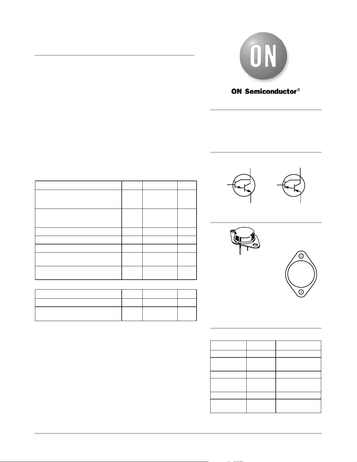
NPN PNP
COLLECTOR
CASE
BASE
1
EMITTER 2
MJ11016 MJ11015
MJ11012
1
2
TO−204AA (TO−3)
CASE 1−07
STYLE 1
MJ1101x = Device Code
G= Pb−Free Package
A = Location Code
YY = Year
WW = Work Week
MEX = Country of Orgin
x = 2, 5 or 6
ORDERING INFORMATION
Device Package Shipping
MJ11012 TO−3 100 Units/Tray
MJ11012G TO−3
MJ11015 TO−3 100 Units/Tray
MJ11015G TO−3
MJ11016 TO−3 100 Units/Tray
MJ11016G TO−3
Preferred devices are recommended choices for future use
and best overall value.
(Pb−Free)
(Pb−Free)
(Pb−Free)
COLLECTOR
CASE
BASE
1
EMITTER 2
MARKING
DIAGRAM
MJ1101xG
AYYWW
MEX
100 Units/Tray
100 Units/Tray
100 Units/Tray
© Semiconductor Components Industries, LLC, 2008
September, 2008 − Rev. 5
1 Publication Order Number:
MJ11012/D
MJ11015 (PNP); MJ11012, MJ11016 (NPN)
PNP
COLLECTOR
MJ11015
BASE
≈ 8.0 k ≈ 40
EMITTER
Figure 1. Darlington Circuit Schematic
ELECTRICAL CHARACTERISTICS (T
Characteristics
OFF CHARACTERISTICS
Collector−Emitter Breakdown Voltage(1)
(I
= 100 mAdc, IB = 0) MJ11012
C
Collector−Emitter Leakage Current
(V
= 60 Vdc, RBE = 1k ohm) MJ11012
CE
= 120 Vdc, RBE = 1k ohm) MJ11015, MJ11016
(V
CE
(V
= 60 Vdc, RBE = 1k ohm, TC = 150_C) MJ11012
CE
(V
= 120 Vdc, RBE = 1k ohm, TC = 150_C) MJ11015, MJ11016
CE
Emitter Cutoff Current
(V
= 5 Vdc, IC = 0)
BE
Collector−Emitter Leakage Current
(V
= 50 Vdc, IB = 0)
CE
ON CHARACTERISTICS(1)
DC Current Gain
(I
= 20 Adc,VCE = 5 Vdc)
C
= 30 Adc, VCE = 5 Vdc)
(I
C
Collector−Emitter Saturation Voltage
(I
= 20 Adc, IB = 200 mAdc)
C
= 30 Adc, IB = 300 mAdc)
(I
C
Base−Emitter Saturation Voltage
(I
= 20 A, IB = 200 mAdc)
C
= 30 A, IB = 300 mAdc)
(I
C
DYNAMIC CHARACTERISTICS
Current−Gain Bandwidth Product
(I
= 10 A, VCE = 3 Vdc, f = 1 MHz)
C
(1) Pulse Test: Pulse Width = 300 μs, Duty Cycle v 2.0%.
= 25_C unless otherwise noted.)
C
NPN
MJ11012
MJ11016
BASE
≈ 8.0 k ≈ 40
MJ11015, MJ11016
COLLECTOR
EMITTER
Symbol
V
(BR)CEO
I
CER
I
EBO
I
CEO
h
FE
V
CE(sat)
V
BE(sat)
h
fe
Min
60
120
−
−
−
−
−
−
1000
200
−
−
−
−
4
Max
−
−
1
1
5
5
5
1
−
−
3
4
3.5
5
−
Unit
Vdc
mAdc
mAdc
mAdc
−
Vdc
Vdc
MHz
http://onsemi.com
2
 Loading...