


XL-HP515
SERVICE MANUAL
No. S4422XLHP515U
MICRO COMPONENT SYSTEM
MODEL XL-HP515
XL-HP515 Micro Component System consisting of XL-
HP515 (main unit) and CP-HP515 (speaker system).
• In the interests of user-safety the set should be restored to its original condition and only parts identical to those specified be used.
CONTENTS
CHAPTER 1. GENERAL DESCRIPTION |
|
CHAPTER 6. CIRCUIT SCHEMATICS AND PARTS |
||
[1] IMPORTANT SERVICE NOTES (FOR |
|
LAYOUT |
|
|
|
U.S.A. ONLY) ................................................ |
1-1 |
[1] NOTES ON SCHEMATIC DIAGRAM ............ |
6-1 |
[2] |
SPECIFICATIONS ........................................ |
1-1 |
[2] TYPES OF TRANSISTOR AND LED ............ |
6-1 |
[3] |
NAMES OF PARTS....................................... |
1-2 |
[3] WIRING SIDE OF PWB/SCHEMATIC DIA- |
|
CHAPTER 2. ADJUSTMENTS |
|
GRAM............................................................ |
6-2 |
|
|
|
|
||
[1] |
ADJUSTMENT .............................................. |
2-1 |
[2] |
TEST MODE ................................................. |
2-3 |
[3]Standard Specification of Stereo System
Error Message Display Contents .................. |
2-5 |
CHAPTER 3. MECHANICAL DESCRIPTION
[1]REMOVING AND REINSTALLING THE
|
MAIN PARTS ................................................ |
3-1 |
[2] |
DISASSEMBLY ............................................. |
3-3 |
CHAPTER 4. DIAGRAMS |
|
|
[1] |
BLOCK DIAGRAM ........................................ |
4-1 |
CHAPTER 5. CIRCUIT DESCRIPTION |
|
|
[1] WAVEFORMS OF CD CIRCUIT ................... |
5-1 |
|
[2] |
VOLTAGE...................................................... |
5-2 |
CHAPTER 7. FLOWCHART |
|
|
[1] |
TROUBLESHOOTING .................................. |
7-1 |
CHAPTER 8. OTHERS |
|
|
[1] FUNCTION TABLE OF IC ............................. |
8-1 |
|
[2] |
FL DISPLAY ................................................ |
8-11 |
Parts Guide
This document has been published to be used SHARP CORPORATION for after sales service only.
The contents are subject to change without notice.
XL-HP515
CHAPTER 1. GENERAL DESCRIPTION
FOR A COMPLETE DESCRIPTION OF THE OPERATION OF THIS UNIT, PLEASE REFER TO THE OPERATION MANUAL.
[1] IMPORTANT SERVICE NOTES (FOR U.S.A. ONLY)
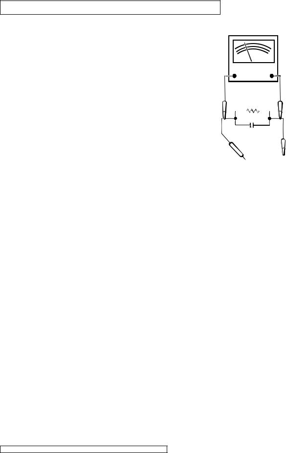
BEFORE RETURNING THE AUDIO PRODUCT
(Fire & Shock Hazard)
Before returning the audio product to the user, perform the following safety checks.
1.Inspect all lead dress to make certain that leads are not pinched or that hardware is not lodged between the chassis and other metal parts in the audio product.
2.Inspect all protective devices such as insulating materials, cabinet, terminal board, adjustment and compartment covers or shields, mechanical insulators etc.
3.To be sure that no shock hazard exists, check for leakage current in the following manner.
*Plug the AC line cord directly into a 120 volt AC outlet.
*Using two clip leads, connect a 1.5k ohm, 10 watt resistor paralleled by a 0.15µF capacitor in series with all exposed metal cabinet parts and a known earth ground, such as conduit or electrical ground connected to earth ground.
*Use a VTVM or VOM with 1000 ohm per volt, or higher, sensitivity to measure the AC voltage drop across the resistor (See diagram).
*Connect the resistor connection to all exposed metal parts having a return path to the chassis (antenna, metal cabinet, screw heads, knobs and control shafts, escutcheon, etc.) and measure the AC voltage drop across the resistor.
VTVM
 AC SCALE
1.5k ohms
10W
0.15 µ F |
|
|
TEST PROBE |
CONNECT TO |
|
TO EXPOSED |
KNOWN EARTH |
|
METAL PARTS |
||
GROUND |
||
|
All check must be repeated with the AC line cord plug connection reversed.
Any reading of 0.3 volt RMS (this corresponds to 0.2 milliamp. AC.) or more is excessive and indicates a potential shock hazard which must be corrected before returning the audio product to the owner.
[2]SPECIFICATIONS
General
Power source |
AC 120 V, 60 Hz |
Power |
80 W |
consumption |
|
|
|
Dimensions |
Width: 7-1/4" (185 mm) |
|
Height: 10-1/4" (260 mm) |
|
Depth: 12" (307 mm) |
|
|
Weight |
13.7 lbs. (6.2 kg) |
|
|
Amplifier
Output power |
75 watts minimum RMS per channel into 6 |
|
ohms from 100 Hz to 20 kHz, 10% total har- |
|
monic distortion |
|
|
Output terminals |
Speakers: 6 ohms |
|
Headphones: 16 - 50 ohms (recommended: |
|
32 ohms) |
|
Subwoofer pre-out (audio signal): |
|
200 mV/10 k ohms at 70 Hz |
|
|
Input terminals |
Video/Auxiliary (audio signal): 500 mV/47 k |
|
ohms |
|
|
CD player
Type |
5-disc multi-play compact disc player |
Signal readout |
Non-contact, 3-beam semiconductor laser |
|
pickup |
|
|
D/A converter |
1-bit D/A converter |
Frequency |
20 - 20,000 Hz |
response |
|
|
|
Dynamic range |
90 dB (1 kHz) |
|
|
Specifications for this model are subject to change without prior notice.
Tuner
Frequency range |
FM: 87.5 - 108 MHz |
|
AM: 530 - 1,720 kHz |
|
|
Cassette deck
Frequency |
50 - 14,000 Hz (normal tape) |
response |
|
|
|
Signal/noise ratio |
50 dB (recording/playback) |
|
|
Wow and flutter |
0.3 % (WRMS) |
|
|
Speaker
Type |
2-way type speaker system |
|
2" (5 cm) tweeter |
|
5-1/8" (13 cm) woofer |
|
|
Maximum input |
150 W |
power |
|
|
|
Rated input power |
75 W |
|
|
Impedance |
6 ohms |
|
|
Dimensions |
Width: 6-1/2" (165 mm) |
|
Height: 10-1/4" (261 mm) |
|
Depth: 9-11/16" (246 mm) |
|
|
Weight |
6.2 lbs. (2.8 kg)/each |
|
|
1 – 1

XL-HP515
[3] NAMES OF PARTS
Front panel
1
2
3
4
5
6
7
8
9
10 |
1. Disc Trays |
|
2. Timer Indicator |
||
|
3. Power On/Stand-by Button |
|
11 |
4. Clock/Timer Button |
|
5. CD Track Down or Fast Reverse, Tape Fast Wind, |
||
12 |
Tuner Preset Down, Time Down Button |
|
6. Tape Reverse Play Button |
||
13 |
7. Tape Reverse Mode Select Button |
|
8. Cassette Compartment |
||
14 |
||
9. Headphone Jack |
||
15 |
10. Disc Tray Open/Close Button |
|
16 |
11. Disc Number Select Buttons |
|
12. CD Direct Play Button |
||
17 |
13. Illumination Light |
|
18 |
14. Volume Control |
|
15. CD Track Up or Fast Forward, Tape Fast Wind, |
||
19 |
Tuner Preset Up, Time Up Button |
|
16. Memory/Set Button |
||
20 |
||
17. Equalizer Mode Select Button |
||
|
18. Extra Bass/Demo Mode Button |
|
|
19. CD Play or Repeat, Tape Forward Play Button |
20. CD or Tape Stop Button
21. CD Button
22. Tuner (Band) Button
23. Tape Button
24. Video/Auxiliary Button
25. Tape Record Pause Button
26. Tuning Up Button
27. Tuning Down Button
|
|
25 |
21 |
23 |
26 |
22 |
24 |
27 |
|
1 |
2 3 4 |
5 |
6 |
7 |
|
■ Display |
|
|
8 9 10 |
1. Disc Number Indicators |
|
|
|||||
|
|
|
|
|
|
|
||
|
|
|
|
|
|
2. CD Play Indicator |
|
|
|
|
|
|
|
|
3. CD Pause Indicator |
|
|
|
|
|
|
|
|
4. Memory Indicator |
|
|
|
|
|
|
|
|
5. CD Repeat Play Indicator |
|
|
|
|
|
|
14 |
11 12 13 |
6. CD Indicator |
|
|
|
|
|
|
7. Extra Bass Indicator |
|
|
||
|
|
|
|
|
|
8. Tape Reverse Play Indicator |
|
|
|
|
|
|
|
|
9. Tape Forward Play Indicator |
|
|
|
|
|
|
|
|
10. Tape Reverse Mode Indicator |
|
|
|
|
|
15 16 17 |
|
11. FM Stereo Mode Indicator |
|
|
|
|
|
|
|
|
|
12. Daily Timer Indicator |
|
|
|
|
|
|
|
|
13. FM Stereo Receiving Indicator |
|
|
|
|
|
|
|
|
14. Tape Record Indicator |
|
|
|
|
|
|
|
|
15. Sleep Indicator |
|
|
|
|
|
|
|
|
16. Timer Play Indicator |
|
|
|
|
|
|
|
4 |
17. Timer Recording Indicator |
|
|
|
|
|
|
|
■ Rear panel |
|
|
|
|
|
|
|
|
5 |
|
|
|
|
|
|
|
|
1. Cooling Fan |
|
|
|
|
|
|
|
|
6 |
|
|
|
|
|
|
|
|
2. Speaker Terminals |
|
|
|
|
|
|
|
|
|
3. AC Power Cord |
|
|
|
|
|
|
|
7 |
4. FM 75 Ohms Antenna Terminal |
|
|
|
1 |
|
|
|
5. FM Antenna Ground Terminal |
|
|
|
|
|
|
|
|
6. AM Loop Antenna Jack |
|
|
|
|
|
|
|
|
|
7. Video/Auxiliary (Audio Signal) Input Jacks |
|
|
|
|
|
|
|
|
8. Subwoofer Pre-output Jack |
|
|
|
2 |
|
|
|
8 |
■ Speaker system |
|
|
|
|
|
|
1. Tweeter |
|
|
||
|
|
|
|
|
|
|
||
|
|
|
|
|
|
2. Woofer |
1 |
3 |
|
|
|
|
|
|
3. Bass Reflex Duct |
||
3 |
4. Speaker Wire |
|
2
4
1 – 2
XL-HP515
1 |
|
|
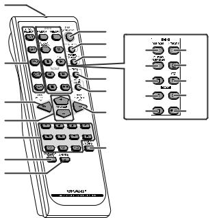
Remote control |
|
|
|
|
||
|
|
|
1. Remote Control Transmitter |
|
8 |
|
|
2. Disc Number Select Buttons |
|
|
|
3. CD Track Down or Fast Reverse, Tape Fast Wind, |
||
9 |
|
|
Tuner Preset Down, Time Down Button |
|
15 |
20 |
4. Volume Up and Down Buttons |
||
10 |
||||
|
|
5. Disc Direct Search Buttons |
||
2 |
16 |
21 |
6. Equalizer Mode Select Button |
|
11 |
17 |
22 |
7. Extra Bass Button |
|
8. Power On/Stand-by Button |
||||
12 |
18 |
23 |
9. CD Button |
|
3 |
10. Tuner (Band) Button |
|||
19 |
24 |
11. Tape Button |
||
13 |
||||
12. Video/Auxiliary Button |
||||
4 |
|
|
13. CD Track Up or Fast Forward, Tape Fast Wind, |
|
5 |
|
|
Tuner Preset Up, Time Up Button |
|
|
|
14. Clock/Timer Button |
||
14 |
|
|
15. CD Random Button |
|
6 |
|
|
16. CD Clear/Dimmer Button |
|
|
|
17. CD Stop Button |
||
|
|
|
||
7 |
|
|
18. Tape Reverse Play Button |
|
|
|
|
19. Tape Stop Button |
|
|
|
|
20. Memory/Set Button |
|
|
|
|
21. CD Pause Button |
|
|
|
|
22. CD Play or Repeat Button |
|
|
|
|
23. Tape Forward Play Button |
|
|
|
|
24. Tape Record Pause Button |
1 – 3
CHAPTER 2. ADJUSTMENTS
[1] ADJUSTMENT
1. MECHANISM SECTION
• Driving Force Check
Torque Meter |
Specified Value |
|
Play: TW-2111 |
Over 80 g |
|
• Torque Check |
|
|
|
|
|
Torque Meter |
Specified Value |
|
Play: TW-2111 |
30 to 80 g.cm |
|
Fast forward: TW-2231 |
70 to 180 g.cm |
|
Rewind: TW-2231 |
70 to 180 g.cm |
|
2. TUNER SECTION fL: Low-range frequency fH: High-range frequency
• AM IF/RF
Signal generator: 400 Hz, 30%, AM modulated
Test Stage |
|
Frequency |
|
Frequency |
|
Setting/ |
Instrument |
||||
|
|
|
|
|
|
|
Display |
|
Adjusting |
Connection |
|
|
|
|
|
|
|
|
|
|
|
Parts |
|
AM IF |
|
450 kHz |
|
1,602 kHz |
|
T351 |
*1 |
||||
AM Band |
|
— |
|
|
|
531 kHz |
|
(fL): T306 |
*2 |
||
Coverage |
|
|
|
|
|
|
|
|
1.1 ± 0.1 V |
|
|
AM Tracking |
|
990 kHz |
|
990 kHz |
|
(fL): T303 |
*1 |
||||
*1. Input: Antenna |
Output: TP302 |
|
|
|
|||||||
*2. Input: Antenna |
Output: TP301 |
|
|
|
|||||||
• FM RF |
|
|
|
|
|
|
|
|
|
|
|
Signal generator: 1 kHz, 40 kHz dev., FM modulated |
|
||||||||||
|
|
|
|
|
|
|
|
|
|
|
|
Test Stage |
|
Frequency |
|
Frequency |
|
Setting/ |
Instrument |
||||
|
|
|
|
|
|
|
Display |
|
Adjusting |
Connection |
|
|
|
|
|
|
|
|
|
|
|
Point |
|
FM Band |
|
— |
|
|
|
87.50 kHz |
|
T301 (fL): |
*1 |
||
Coverage |
|
|
|
|
|
|
|
|
1.3 ± 0.1 V |
|
|
FM RF |
|
98.00 MHz |
|
98.00 MHz |
|
L312 |
*2 |
||||
|
|
|
(10-30 dB) |
|
|
|
|
|
|
||
*1. Input: Antenna |
Output: TP301 |
|
|
|
|||||||
*2. Input: Antenna |
Output: Speaker terminal |
|
|||||||||
• FM IF |
|
|
|
|
|
|
|
|
|
|
|
Signal generator: 10.7MHz FM modulated |
|
|
|
||||||||
|
|
|
|
|
|
|
|
|
|||
Test Stage |
|
Frequency |
|
Frequency |
|
|
Setting/ |
Instrument |
|||
|
|
|
|
|
|
|
Display |
|
|
Adjusting |
Connection |
|
|
|
|
|
|
|
|
|
|
Point |
|
IF |
|
10.7 MHz |
|
98 MHz |
|
T302 |
*1 |
||||
|
|
|
|
|
|
|
|
|
(Turn the |
|
|
|
|
|
|
|
|
|
|
|
core of trans- |
|
|
|
|
|
|
|
|
|
|
|
former T302 |
|
|
|
|
|
|
|
|
|
|
|
fully counter- |
|
|
|
|
|
|
|
|
|
|
|
clock wise) |
|
|
*1. Input: Antenna |
Output: TP301 |
|
|
|
|||||||
XL-HP515
• Tape Speed
|
Test Tape |
Adjusting |
Specified |
Instrument |
|
|
|
Point |
Value |
|
Connection |
Normal |
MTT-111 |
Variable |
3,000 ± 30 |
Hz |
Speaker Ter- |
speed |
|
Resistor in |
|
|
minal (Load |
|
|
motor. |
|
|
resistance: 6 |
|
|
|
|
|
ohms) |
TAPE MECHANISM
Tape
Motor 
Variable Resistor in motor
Figure 1
|
|
SO302 |
|
|
|
|
|
FM ANTENNA |
AM |
||
|
|
TERMINAL |
|
||
|
|
|
|
LOOP |
|
TUNER PWB-C |
|
|
ANTENNA |
||
|
|
|
|
||
|
|
|
|
CNP301 |
|
|
|
|
|
AM TRACKING fL |
|
|
|
IC301 |
|
|
|
|
|
|
L312 |
|
T303 |
|
|
|
|
|
|
|
TP301 |
|
|
T306 |
|
|
|
FM RF |
|
|
|
20 |
C393 |
T302 |
|
|
|
IC302 |
|
|
|
|
|
|
T301 |
|
AM BAND |
||
|
|
FM IF |
|
||
|
|
|
|
COVERAGE fL |
|
|
|
FM OSC |
|
|
|
|
T351 |
|
IC303 |
|
|
|
AM IF |
|
|
||
|
|
R356 |
|
||
|
|
|
|
TP302 |
|
|
|
|
|
|
|
Figure 2 ADJUSTMENT POINTS
3. CD SECTION
•Adjustment
Since this CD system incorporates the following automatic adjustment functions, readjustment is not needed when replacing the pickup. Therefore, different PWBs and pickups can be combined freely.
Each time a disc is changed, these adjustments are performed automatically. Therefore, playback of each disc can be performed under optimum conditions.
Items adjusted automatically
1)Offset adjustment (The offset voltage between the head amplifier output and the VREF reference voltage is compensated inside the IC.)
*Focus offset adjustment
*Tracking offset adjustment
2 – 1
XL-HP515
2)Tracking balance adjustment
3)Gain adjustment (The gain is compensated inside the IC so that the loop gain at the gain crossover frequency will be 0 dB.)
*Focus gain adjustment
*Tracking gain adjustment
4. CD ERROR CODE DESCRIPTION
Error |
Explanation |
01 |
When Pickup set inner position, inner switch cannot detect |
|
'ON' level for 10 secs. |
10* |
CAM error. Can't detect CAM switch when CAM is moving. |
11* |
When it detect cam operation error during initialize process. |
20* |
TRAY error. Can't detect TRAY switch when TRAY is mov- |
|
ing. |
21* |
When it detect TRAY operation error during initialize pro- |
|
cess. |
31 |
When it change to CD function, DSP cannot read initial data. |
*'CHECKING'
If Error is detected, 'CHECKING' will be displayed instead of 'ERCD**'. 'ER-CD**' display will only be displayed when error had been detected for the 5th times.
2 – 2
XL-HP515
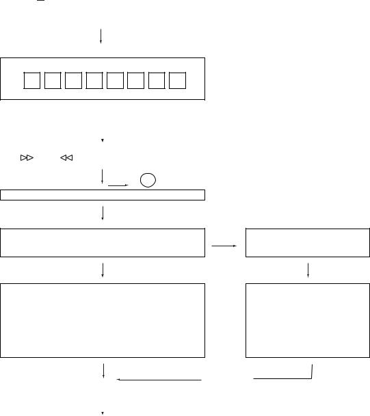
[2] TEST MODE
• Setting the test mode
During stand-by mode, press ON/STAND-BY button while pressing
down the 
 button and X-BASS/DEMO button. then, press the CD button to enter the test mode.
C D |
T E S T |
IL isn’t done
|
OPEN/CLOSE operation is using manual. |
IL isn’t done |
|||
|
|
|
|
IL isn’t done |
|
|
|
|
|
||
|
|
|
|
||
<< |
>>,<< |
>>buttons make pick's slide possible. |
|||
|
|||||
A to page 2-4
<<PLAY>> key input.
Do TOC IL. Do normal play.
When these following key is input into PLAY key, track number can be appoint directly.
<<
 1>> key: Track 4
<<
 2>> key: Track 9
<<
 3>> key: Track 15
––––––––
|
<<STOP>> key input. |
|
|
|
|
|
|
|
|
|
|
|
STOP |
|
explanation: |
|
|
a) Focus off set |
= "FOF_XXXX" |
|
b)Tracking off set |
= "TOF_XXXX" |
|
c)Tracking balance |
= "TBAL_XX" |
|
d)Tracking Gain |
= "TGAN_XX" |
|
f) Focus Gain |
= "FGAN_XX" |
|
g) RF level shift |
= "RFLS_XX" |
|
VOL — Last memory
P.GEQ — FLAT
X-BASS — OFF
To cancel : Power OFF
<<MEMORY>> key input.
Adjustment result automatically will display as below for each 2 sec:
a)"FOF_XXXX"
b)"TOF_XXXX"
c)"TBAL_XX"
d)"TGAN_XX"
f)"FGAN_XX"
g)"RFLS_XX"
2 – 3
XL-HP515
A
<<MEMORY>> key input.
Laser ON.
<<MEMORY>> key input.
Tracking OFF play at that specific point.
<<MEMORY>> key input.
Tracking ON play from that specific point.
<<MEMORY>> key input.
Adjustment result automatically will display as below for each 2 sec :
a)"FOF_XXXX"
b)"TOF_XXXX"
c)"TBAL_XX"
d)"TGAN_XX"
f)"FGAN_XX"
g)"RFLS_XX"
<<STOP>> key input.
STOP
Sliding the PICKUP with<<  >>, <<
  >> button must only be in STOP mode.
explanation: |
|
a) Focus off set |
= "FOF_XXXX" |
b)Tracking off set |
= "TOF_XXXX" |
c)Tracking balance |
= "TBAL_XX" |
d)Tracking Gain |
= "TGAN_XX" |
f) Focus Gain |
= "FGAN_XX" |
g) RF level shift |
= "RFLS_XX" |
VOL — Last memory |
|
P.GEQ — FLAT |
|
X-BASS — OFF |
|
To cancel : Power OFF |
|
2 – 4
XL-HP515
[3] Standard Specification of Stereo System Error Message Display Contents
|
Error Contents |
|
DISPLAY |
Notes |
|
CD |
Pickup Mechanism Error. |
'ER-CD01' |
|
PU-IN SW Detection NG. |
|
|
CD Changer Mechanism Error. |
'ER-CD**' (*) |
|
10: CAM SW Detection NG during normal operation |
|
|
|
|
|
|
11: CAM SW Detection NG during initialize process |
|
|
|
|
|
20:TRAY SW Detection NG during normal operation |
|
|
|
|
|
21:TRAY SW Detection NG during initialize process |
|
CD DSP Communication Error. |
'ER-CD31' |
|
DSP COMMUNICATION ERROR. |
|
|
Focus Not Match/IL Time Over. |
'NO DISC' |
|
|
|
TUNER |
PLL Unlock. |
|
87.50 |
|
PLL Unlock. |
|
|
FM |
MHz |
|
|
|
|
|
|
||
(*) CHECKING:
If CD changer mechanism error is detected, 'CHECKING' will be display instead of 'ER-CD**'. 'ER-CD**' display will only be display when error had been detected for the 5 th times.
Speaker abnormal detection and +B PROTECTION display
In case speaker abnormal detection or +B PROTECTION had occurred, it can be check by pressing 'POWER', '  ' and 'X-BASS' button. MicroComputer version number will displayed as "U******".
Press ‘VIDEO/AUX’ button during version number display and then press ‘POWER’, ‘MEMORY/SET’ and ‘VIDEO/AUX’ button. Display will show "S** B**". S is referring to speaker abnormal detection and B is referring to +B PROTECTION. ** is in hex valve.
+B PROTECTION is condition when irregular process occur on power supply line. BEFORE TRANSPORTING THE UNIT
The following process need to be taken after set tapering/parts replacement.
1.Press the ON/STAND-BY button to enter stand-by mode.
2.While pressing down the  button and the X-BASS/DEMO button, press the ON/STAND-BY button. The Micro Computer version number will be displayed as "U******".
3.Press OPEN/CLOSE button until "WAIT"--> "FINISHED" appears.
4.Unplug the AC cord and the unit is ready for transporting.
2 – 5
XL-HP515
CHAPTER 3. MECHANICAL DESCRIPTION
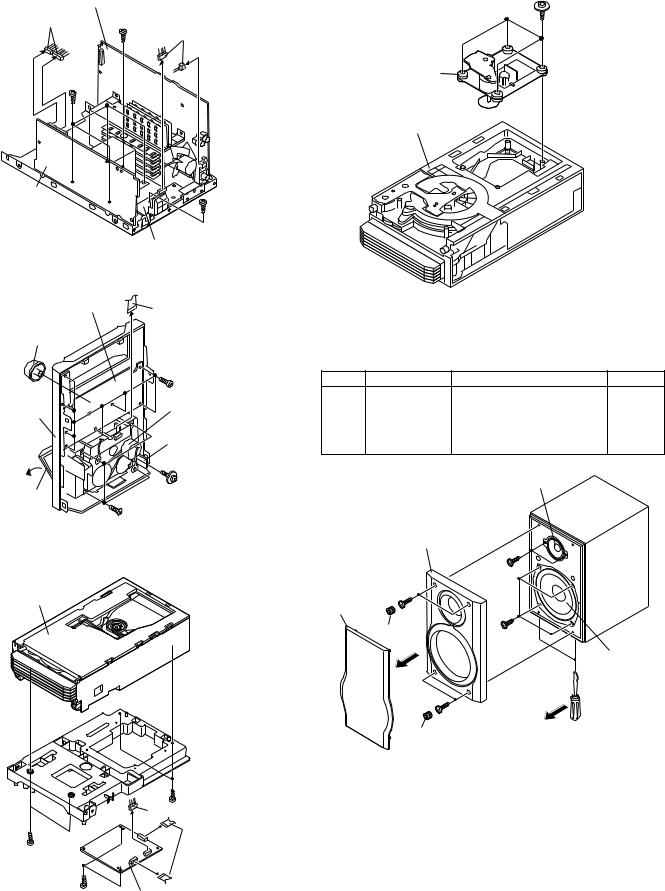
[1] REMOVING AND REINSTALLING THE MAIN PARTS
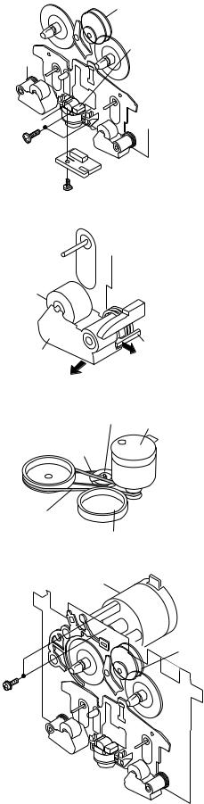
1. TAPE MECHANISM SECTION
Perform steps 1 to 9 of the disassembly method to remove the tape mechanism.(see page 3-3,3-4)
1.1. How to remove the Record/Playback Head (See Fig. 1)
1.When you remove the screws (A1) x 2 pcs and (A2) x 1 pc., the record/playback head can be removed.
1.2. How to remove the Pinch Roller (See Fig. 2)
1.Carefully bend the pinch roller pawl in the direction of the arrow <A>, and remove the pinch roller (B1) x 1 pc., in the direction of the arrow <B>.
NOTE: When installing the pinch roller, pay attention to the spring mounting position.
1.3. How to remove the Belt (See Fig. 3)
1.Remove the main belt (C1) x 1 pc., from the motor side.
2.Remove the FF/REW belt (C2) x 1 pc.
1.4. How to remove the Motor (See Fig. 4)
1. Remove the screws (D1) x 2 pcs., to remove the motor.
Clutch Ass'y
Record/Playback
Head
Erase Head
(A1)x2
Ø2x6mm
(A2)x1
Ø2x9mm
Figure 1
|
|
Pinch |
|
Pinch Roller |
<A> |
Roller |
|
Pawl |
|||
(B1)x1 |
|||
|
|
||
Pull |
<B> |
|
|
|
|
Figure 2
FF/REW
Clutch Motor
FF/REW Belt (C2)x1
Main Belt (C1)x1
Flywheel
Figure 3
Motor
Clutch Ass'y
(D1)x2 Ø2.6x5mm
Figure 4
3 – 1
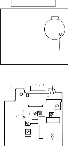
2. CD MECHANISM SECTION
Perform steps 1 to 4 and 11 to 12 of the disassembly method to remove the CD mechanism.(see page 3-3,3-4)
2.1. How to remove the Optical Pickup (See Fig. 1)
1.Remove the stop washer (A1) x 1 pc and gear (A2) x 1 pc.
2.Remove the screws (A3) x 2 pcs and shaft (A4) x 1 pc.
3.Remove the optical pickup.
NOTE: After pulling out the optical pickup connector, wrap the tip of it with conductive aluminium foil or the like to protect the optical pickup from the static electricity.
2.2. How to remove CD Disc (See Fig. 2~6)
1.When CD is at play position, rotate reduction gear C clock-wise as shown in Figure 2 Until disk tray is at ‘STOCK’ position, then rotate the gear further to eject the disk tray (Figure 6) so that CD can be removed from the tray.
2.In another case, if CD mechanism is at tray No. 1 play position and to remove CD located in tray No. 3, the procedure is as follows:
If the gear up down board is located at tray No. 1 position, then rotate Reduction gear C clock-wise until Disc tray is at stalk ‘STOCK’ position. Rotate reduction gear D clock-wise (Figure 3) to move the CD mechanism to tray No. 3 position. This is confirmed by checking the gear up down board position Base on the marking as indicated on the main chassis as shown in Figure 4.
•Usually changer is covered with top plate. As for reference purpose, we exclude the top plate for easy viewing. (Figure 5,6)
CD Disc
Disc Tray
Guide Tray
CD At 'PLAY' position.
CD Disc
CD At 'STOCK' position.
Figure 5
CD Disc
Remove CD from tray.
Tray eject
Figure 6
XL-HP515
(A3) x2
ø2.6 x5mm 
Stop Washer (A1) x1
Optical Pickup
CD
Mechanism
Shaft Gear (A4) x1 (A2) x1
Figure 1
Reduction gear C
Front Rear
Figure 2
Reduction gear D
Up Down
Figure 3
Gear up down board
|
|
|
|
|
|
Mark 1 |
Mark 3 |
Mark 5 |
|||
(DISC 1) |
(DISC 3) |
(DISC 5) |
|||
|
Mark 2 |
Mark 4 |
|||
|
(DISC 2) |
(DISC 4) |
|||
Figure 4
3 – 2
XL-HP515
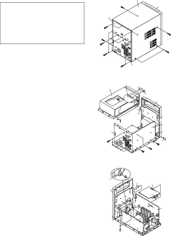
[2] DISASSEMBLY
Caution on Disassembly
Follow the below-mentioned notes when disassembling the unit and reassembling it, to keep it safe and ensure excellent performance:
1)Take cassette tape and compact disc out of the unit.
2)Be sure to remove the power supply plug from the wall outlet before starting to disassemble the unit.
3)Take off nylon bands or wire holders where they need to be removed when disassembling the unit. After servicing the unit, be sure to rearrange the leads where they were before disassembling.
4)Take sufficient care on static electricity of integrated circuits and other circuits when servicing.
STEP |
REMOVAL |
|
PROCEDURE |
|
FIGURE |
1 |
Cabinet |
1. |
Screw.......................... |
(A1) x11 |
1 |
2 |
Rear Panel Top |
1. |
Screw............................ |
(B1) x2 |
1 |
3 |
CD Changer unit |
1. |
Hook............................. |
(C1) x2 |
2 |
|
|
2. |
Socket.......................... |
(C2) x1 |
|
|
|
3. |
Flat Cable..................... |
(C3) x1 |
|
4 |
Rear Panel Bot- |
1. |
Screw........................... |
(D1) x9 |
2 |
|
tom |
|
|
|
|
5 |
Front Panel |
1. |
Screw........................... |
(E1) x3 |
2,3 |
|
|
2. |
Flat Cable.................... |
(E2) x2 |
|
|
|
3. |
Socket.......................... |
(E3) x1 |
3 |
|
|
4. |
Hook............................ |
(E4) x2 |
|
6 |
Turner PWB |
1. Screw............................ |
(F1) x1 |
2 |
|
|
|
2. |
Socket.......................... |
(F2) x1 |
3 |
7 |
Main PWB |
1. |
Screw........................... |
(G1) x2 |
2,4 |
|
|
2. |
Socket......................... |
(G2) x4 |
4 |
8 |
Power PWB |
1. |
Screw........................... |
(H1) x4 |
4 |
9 |
Terminal PWB |
1. |
Screw............................ |
(J1) x1 |
4 |
10 |
Display PWB |
1. |
Knob............................. |
(K1) x1 |
5 |
|
|
2. |
Screw........................... |
(K2) x 8 |
|
|
|
3. |
Flat Cable.................... |
(K3) x 1 |
|
11 |
Tape Mechanism |
1. |
Screw........................... |
(L1) x 4 |
5 |
12 |
Headphones PWB |
1. Screw.......................... |
(M1) x 1 |
5 |
|
13 |
CD Servo PWB |
1. Screw........................... |
(N1) x2 |
6 |
|
|
(Note 1) |
2. |
Flat Cable................... |
(N2) x 2 |
|
|
|
3. |
Socket.......................... |
(N3) x1 |
|
14 |
CD Mechanism |
1. Screw........................... |
(P1) x4 |
6 |
|
|
|
2. |
Screw........................... |
(P2) x4 |
7 |
Note 1:
After removing the connector for the optical pickup from the connector, wrap the conductive aluminium foil around the front end of the connector so as to protect the optical pickup from electrostatic damage.
Cabinet
|
(A1) x1 |
Front Panel |
|
ø3x10mm |
|
|
|
|
Rear |
|
|
Panel Top |
|
|
(A1) x1 |
|
|
ø3x8mm |
|
|
|
|
(A1) x1 |
|
|
ø3x10mm |
(A1) x2 |
|
|
ø3x8mm |
|
|
(B1) x2 |
|
(A1) x2 |
ø3x10mm |
|
ø3x8mm |
(A1) x2 |
|
|
ø3x8mm |
|
|
|
(A1) x2 |
|
|
ø3x8mm |
|
|
Rear |
|
|
Panel Bottom |
|
|
Figure 1 |
|
|
CD Servo PWB |
|
CD Changer |
(C3) x1 |
|
|
|
|
Unit |
|
|
|
|
(C2) x1 |
|
|
Front Panel |
|
Pull |
|
|
Hook |
Hook |
|
(C1)x1 |
|
|
(C1)x1 |
|
|
|
|
|
|
Pull |
|
|
Main PWB |
Rear |
|
Headphones |
Panel Bottom |
|
|
|
PWB |
|
|
|
(D1) x9 |
(E2) x1 |
|
|
ø3x8mm |
(E1) x1 |
|
|
|
ø3x10mm |
|
(F1) x1 |
|
(G1) x1 ø3x8mm |
|
ø3x10mm |
Figure 2
|
x1 |
Tape |
(E2) x1 |
Mechanism |
|
|
(F2) x1 |
Front Panel
Hook (E4)x1
Turner PWB
Pull
Main PWB
Hook (E4)x1
Pull
 (E1) x2 ø3x10mm
Figure 3
3 – 3
XL-HP515
Main PWB |
(P2) x4 |
|
|
(G1) x1 |
|
(G2) x2 |
ø3x6mm |
ø2.6x10mm |
|
|
(G2) x2 |
(H1) x4 |
|
CD Mechanism |
ø4x6mm |
|
|
CD Changer
Unit
Power PWB |
|
(J1) x1 |
|
|
|
|
|
ø3x6mm |
|
Terminal PWB |
|
Figure 4 |
|
|
Display PWB |
(K3) x1 |
Figure 7 |
|
||
|
|
|
(K1) x1 |
|
|
Front Panel
Cassette
Holder
CD Changer
Unit
(P1) x2 ø3x10mm
(K2) x8 |
|
|
|
|
|
|
ø2.6x8mm |
STEP |
REMOVAL |
|
PROCEDURE |
|
FIGURE |
|
|
|
||||
Tape |
|
Woofer/ |
1. |
Net Frame................ |
(A1) x1 |
8 |
|
Tweeter |
2. |
Catching Holder |
(A2) x4 |
|
|
Mechanism |
|
|
||||
|
|
3. |
Screw |
(A3) x4 |
|
|
Headphones |
|
|
|
|||
|
|
4. |
Front Panel.............. |
(A4) x1 |
|
|
PWB |
|
|
5. |
Screw |
(A5) x6 |
|
|
|
|
|
Tweeter
(M1) x1 ø3x10mm
(L1) x4
ø3x10mm Front Panel ( A4 ) x1
Figure 5
(A3)x2 |
(A5)x2 |
|
ø3.5x14mm |
|
|
ø3.5x16mm |
|
|
|
|
|
Net Frame |
|
|
( A1 ) x1 |
|
|
(A2)x2 |
(A5)x4 |
|
|
|
|
|
ø3.5x14mm |
Woofer |
|
|
|
|
(A3)x2 |
Screwdriver |
|
|
|
(A2)x2 |
ø3.5x16mm |
|
|
|
(P1) x2 |
Figure 8 |
ø3x10mm |
|
(N3) x1
(N2) x2
(N1) x2 |
CD Servo PWB |
ø3x10mm |
|
Figure 6
3 – 4
XL-HP515
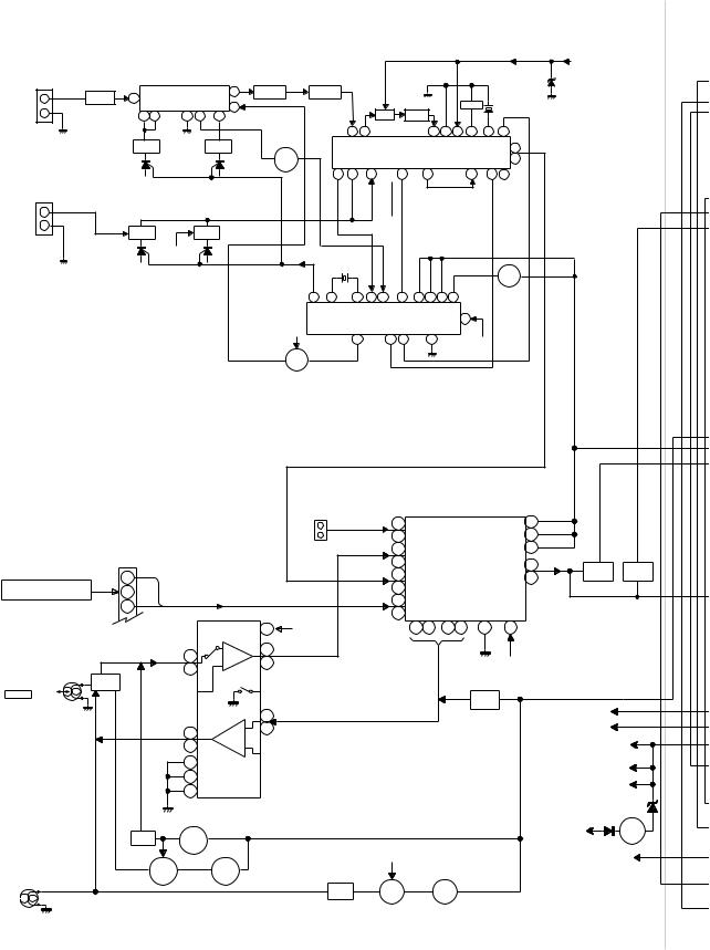
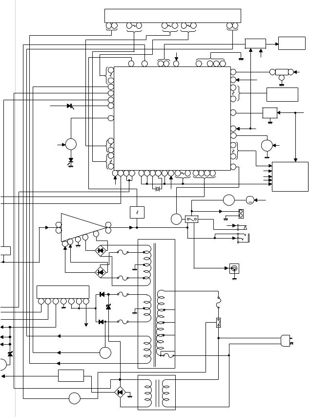
CHAPTER 4. DIAGRAMS
[1] BLOCK DIAGRAM
|
|
|
|
|
IC301 |
|
|
|
|
|
|
|
|
|
|
|
|
|
|
|
|
|
|
|
|
|
|
||
FM ANTENNA |
|
|
|
TA7358AP |
|
|
|
|
|
|
|
|
|
|
|
|
|
|
|
|
|
|
|
|
+B5 |
|
|||
TERMINAL |
|
|
FM FRONT END |
|
FM IF |
|
|
|
|
|
|
|
|
|
10.7 MHz |
|
ZD351 |
|
|
||||||||||
|
SO302 |
B.P.F |
|
|
|
|
|
|
|
|
|
|
|
|
|
|
|
|
|
|
|
||||||||
|
|
|
|
|
|
|
6 |
T302 |
CF302 |
|
|
|
|
|
|
|
|
|
|
|
|
|
5.1V |
|
|
||||
|
|
BF301 |
|
1 |
|
|
|
|
|
|
|
|
|
|
|
|
|
X351 |
|
|
|||||||||
|
|
|
|
|
|
9 |
|
|
|
|
|
|
|
450 kHz |
|
|
CF351 |
|
|
IC303 |
|
||||||||
|
|
|
|
|
|
|
|
|
|
|
|
|
|
T351 |
|
|
456 kHz |
|
|
||||||||||
|
|
|
|
3 |
4 |
5 |
7 |
8 |
|
|
|
|
|
|
CF352 |
|
|
|
|
|
|
|
|
|
LA1832S |
|
|||
|
|
|
|
|
|
|
|
|
AM IF |
|
|
|
|
|
|
|
|
|
|
|
|
||||||||
|
|
|
|
|
|
|
|
|
|
OSC |
|
1 |
|
4 |
5 |
9 |
8 |
17 13 |
|
|
|
FM IF DET. |
|
||||||
|
|
|
|
|
|
|
|
|
|
|
2 |
|
|
|
|
|
|
|
|||||||||||
|
|
FM RF |
L312 |
|
T301 |
|
BUFF |
|
|
AM MIX OUT |
|
|
|
AMIF |
GND |
FM+B |
FM DET |
VCO FM/AM |
MO/ST |
L 14 |
|
FM MPX./AM IF |
|||||||
|
|
|
|
|
|
|
|
|
|
|
|
||||||||||||||||||
|
|
|
|
|
FM OSC |
|
|
Q302 |
|
|
|
|
FM/AM OUT |
MPXIN |
R |
15 |
|
|
|
|
|||||||||
|
|
|
|
|
|
|
|
|
|
|
|
|
|
|
7 |
|
|
|
|
|
|
||||||||
|
|
|
|
|
|
|
|
|
|
|
|
24 |
23 |
21 |
|
|
18 |
|
|
16 |
12 20 |
|
|
|
|
|
|||
CNP301 |
|
|
AM |
|
AM BAND |
|
|
|
AM OSC OUT |
AM OSC IN |
AM RF IN |
|
STEREO |
|
|
|
|
|
|
|
|
|
|
|
|
|
|||
|
2 |
|
|
|
|
|
|
|
|
|
|
|
|
|
|
|
|
|
|
|
|
||||||||
AM LOOP |
|
TRACKING |
COVERAGE |
|
|
|
|
|
|
|
|
|
|
|
|
|
|
|
|
|
|||||||||
ANTENNA |
1 |
|
|
|
|
|
|
|
|
|
|
|
|
|
|
|
|
|
|
|
|
|
|
|
|
|
|
|
|
|
|
|
T303 |
|
|
T306 |
|
|
|
|
|
|
|
|
|
|
|
|
|
|
|
|
|
|
|
|
|
|
|
|
|
|
|
|
|
|
|
|
|
|
|
|
|
|
|
|
|
|
|
|
|
|
|
|
|
|
|
||
|
|
|
|
|
+B6 |
|
|
|
|
VT |
X352 |
|
|
|
|
|
|
|
|
|
|
|
|
|
|
|
|
||
|
|
|
|
|
|
|
|
|
|
|
|
|
|
|
|
|
|
|
|
|
|
|
|
|
|
|
|||
|
|
|
|
|
|
|
|
|
|
|
|
4.5 MHZ |
|
|
|
|
|
|
|
|
Q361 |
|
|
|
|
||||
|
|
|
|
|
|
|
|
|
IC302 |
|
|
|
|
|
|
CE |
DI CLK |
DO |
|
|
|
|
|
|
|||||
|
|
|
|
|
|
|
|
|
|
|
|
|
|
|
|
|
|
|
|
|
|
|
|
||||||
|
|
|
|
|
|
|
|
|
LC72131 |
20 |
1 |
22 15 16 |
11 |
3 |
4 |
5 |
6 |
|
|
|
|
|
|
|
|
|
|||
|
|
|
|
|
|
|
|
PLL(TUNER) |
OSC |
|
FM/AM |
MO/ST |
|
|
|
|
17 |
|
|
|
|
|
|
|
|
||||
|
|
|
|
|
|
|
|
|
|
|
|
|
|
|
|
|
|
|
|
|
|
|
|
|
|
|
|||
|
|
|
|
|
|
|
|
|
|
+B5 |
|
|
|
|
|
|
|
|
|
|
|
|
|
|
|
|
|||
|
|
|
|
|
|
|
|
|
|
|
7 |
9 10 |
|
21 |
|
|
|
|
|
|
|
|
|
|
|
||||
|
|
|
|
|
|
|
|
|
|
|
|
|
|
|
|
+B5 |
|
|
|
|
|
|
|
||||||
|
|
|
|
|
|
|
|
FM+B |
|
Q360 FM |
|
|
|
|
|
|
|
|
|
|
|
|
|
|
|
|
|
|
|
|
|
|
|
|
|
|
|
SWITCHING |
|
|
|
|
|
|
|
|
|
|
|
|
|
|
|
|
|
|
|
||
|
|
|
|
|
|
|
|
|
|
|
JK690 |
|
|
L |
9 |
|
|
|
|
|
|
|
|
DI |
1 |
|
|
|
|
|
|
|
|
|
|
|
|
|
|
|
L |
VIDEO/AUX |
|
|
|
|
|
|
|
|
|
|
SYSTEM MUTE |
||||||
|
|
|
|
|
|
|
|
|
|
|
R |
|
|
|
R 16 |
|
|
|
|
|
|
|
|
CE 2 |
|
|
|||
|
|
|
|
|
|
|
|
|
|
|
|
|
TAPE |
L |
10 |
|
|
|
IC601 |
|
CLK |
24 |
|
ñ20dB |
|||||
|
|
|
CNS2 |
|
|
|
|
|
|
|
|
|
|
|
|
|
|
|
|
|
|
||||||||
|
|
|
|
|
|
|
|
|
|
|
|
|
R |
15 |
|
|
LC75341 |
|
|
|
21 |
R |
ATT Q601 |
Q603 |
|||||
|
|
|
|
|
|
|
|
|
|
|
|
|
|
|
|
|
|
|
|
||||||||||
FROM CD SECTION |
1 |
|
|
|
|
|
|
|
|
|
TUNER |
L 11 |
AUDIO PROCESSOR |
4 |
L |
Q602 |
Q604 |
||||||||||||
2 |
|
|
|
|
|
|
|
|
|
|
|
R 14 |
|
|
|
|
|
|
|
|
|
|
|
|
|
||||
|
CNP2 |
|
|
|
|
|
|
|
|
|
|
|
CD |
L |
12 |
|
|
|
|
|
|
|
|
|
|
|
|
|
|
|
|
|
|
|
|
|
|
|
|
|
|
|
|
|
|
|
|
|
|
|
|
|
|
|
|
||||
|
|
|
3 |
|
|
|
|
|
|
|
|
|
|
|
|
|
|
|
|
|
|
|
|
|
|
|
|||
|
|
|
|
|
|
|
|
|
|
|
|
|
|
R 13 |
|
|
|
|
|
|
|
|
|
|
|
|
|
||
|
|
|
|
|
|
|
|
|
|
|
|
|
|
|
|
|
|
|
|
|
|
|
|
|
|
|
|
||
|
|
|
|
|
|
|
|
|
13 |
|
+B5 |
|
|
|
|
|
7 18 |
8 17 |
3 |
|
23 |
|
|
|
|
||||
|
|
|
|
|
|
|
|
P.B |
|
|
|
|
|
|
|
|
|
|
|
|
|
|
|
|
|
|
|
|
|
|
|
SWITCHING |
L(TA) |
2 |
|
|
4 |
L |
PB |
|
|
|
|
|
|
|
|
|
|
|
|
+B5 |
|
|
|
|
|||
|
|
|
|
21 |
R |
|
|
|
|
|
|
|
|
|
|
|
|
|
|
|
|
|
|||||||
|
|
|
|
|
R(TA) |
23 |
|
|
|
|
|
|
|
|
|
|
|
|
|
|
|
|
|
|
|
||||
|
|
|
|
|
|
|
|
|
|
|
|
|
|
|
|
|
|
|
|
|
|
|
|
|
|
|
|
||
REC /P.B. HEAD |
Q101- |
|
|
|
|
|
|
|
|
|
L-CH |
Q104 |
|
|
|
|
|
|
REC/PLAY |
|
|
TAPE R-CH |
|
|
|
|
|
|
|
Q107 |
|
|
|
|
H/N |
|
L REC |
|
|
|
Q108 |
+B5 |
A_+10V |
AC BIAS |
|
7 |
|
|
|
MUTING |
|
|||
|
|
|
|
|
|
LD_+8V |
||||
|
|
|
18 |
R |
|
|
|
|
+B4 |
|
|
L REC |
9 REC |
|
|
|
|
|
|||
|
|
|
|
|
|
|
|
|
||
|
R REC |
16 |
|
IC101 |
|
|
|
+B7(A_+5V) |
||
|
|
11 |
|
AN7345K |
|
|
+B8(D_+5V) |
|||
|
|
12 |
|
PLAYBACK AND RECORD |
||||||
|
|
|
|
|
|
|||||
|
|
|
/PLAYBACK AMP. |
|
+B9(SW_+5V) |
|||||
|
|
15 |
|
|
||||||
|
|
|
|
|
|
|
|
|
|
|
|
SWITCHING |
|
|
|
|
|
|
|
|
|
|
Q105 |
SWITCHING |
|
|
|
|
|
+B_PROTECT |
|
Q851 |
|
Q114 |
|
|
|
|
|
|
|||
|
Q106 |
|
|
|
|
|
|
|
UNS |
|
|
+B5 |
|
|
|
|
+B5 |
|
|
|
|
|
|
|
|
|
|
|
|
|
+B10 |
|
ERASE |
Q112 |
Q113 |
|
|
|
|
BIAS |
|
|
|
|
|
|
|
|
|
|
|
|
||
HEAD |
SWITCHING |
|
BIAS |
Q111 |
Q109 |
Q110 |
BIAS |
|
|
|
|
|
|
|
OSC |
L103 |
|
|
|
||
|
|
|
|
|
|
|
|
|
||
|
|
|
|
|
|
SWITCHING |
|
|
|
|
Figure 4-1 BLOCK DIAGRAM (1/3)
4 – 1
|
|
|
|
|
|
|
|
|
|
|
|
|
|
|
|
|
|
|
|
|
|
|
|
|
|
XL-HP515 |
|
|
|
|
|
|
|
|
|
|
|
|
|
|
|
|
FL701 |
|
|
|
|
|
|
|
|
|
|
|
|
|
|
|
|
|
|
|
|
|
|
|
|
|
FL DISPLAY |
|
|
|
|
|
|
|
|
|
||
|
|
|
|
|
|
|
1 |
2 |
|
|
5 |
21 |
|
|
28 |
31 |
32 |
41 |
|
|
44 45 |
MOTOR/ |
|
|
|
|
|
|
|
|
|
|
|
|
|
|
|
|
|
|
|
|
|
|
|
|
|
|
|
|
|
|
|
|
|
|
|
|
|
|
|
|
|
|
|
|
|
|
|
|
|
|
|
|
|
|
SOLENOID |
|
|
|
|
|
|
|
|
|
|
|
|
|
|
|
|
|
|
|
|
|
|
|
|
|
|
DRIVER |
|
TAPE |
|
|
|
|
|
|
|
|
|
|
|
|
|
|
|
|
|
|
|
|
|
|
|
|
Q701,702 |
|
||
|
|
|
|
|
|
|
|
|
|
|
|
|
|
|
|
|
|
|
|
|
|
|
|
MECHANISM |
||
|
|
|
|
|
|
|
|
|
|
|
|
|
|
|
|
|
|
|
|
|
|
|
Q712~715 |
|
||
|
|
|
|
|
|
|
|
|
|
|
|
|
|
|
|
|
|
|
|
|
|
|
|
ASS'Y |
||
|
|
|
|
|
|
|
|
|
|
|
|
|
|
|
|
+B10 |
|
|
|
|
|
|
|
|||
|
|
|
|
|
|
|
|
|
|
|
|
|
|
|
|
|
|
|
|
|
|
|
|
|
||
|
|
|
|
|
|
|
|
|
|
|
|
|
|
|
|
|
|
|
|
|
|
|
+B3 |
|
|
|
|
|
|
|
|
|
|
|
|
|
|
|
38 |
|
48 |
43 44 |
46 |
|
59 |
40 25 |
13 |
REMOTE SENSOR |
|
||||
|
|
|
|
|
|
|
69 |
|
|
|
|
|
AC RLY |
T SOL |
MOTOR |
VDD |
|
|
|
|
|
|
||||
|
|
|
|
|
|
|
|
|
|
|
|
|
|
|
REMOCON 39 |
|
1 |
RX701 2 |
+B10 |
|||||||
|
|
|
|
|
|
|
|
|
|
|
|
|
|
|
|
|
|
|||||||||
|
|
|
|
|
|
|
|
|
|
|
|
|
|
|
|
|
|
|
|
|
3 |
|||||
|
|
|
|
|
|
|
78 |
|
|
|
|
|
|
|
|
AVDD 34 |
+B10 |
|
|
|||||||
|
|
|
|
|
|
|
|
|
|
|
|
|
|
|
|
|
|
|||||||||
|
|
|
|
|
|
|
79 VLOAD |
|
|
|
T |
|
|
|
|
|
33 |
|
|
|
|
|||||
|
|
|
|
|
|
|
|
|
|
|
|
|
|
|
|
|
|
KEY |
|
|||||||
|
|
|
|
|
|
|
36 |
P_IN |
|
|
|
|
|
|
|
|
|
|
|
|
|
SW701-SW705 |
|
|||
|
|
|
|
|
|
|
41 |
SMUTE |
|
|
|
|
|
|
|
|
|
31 |
|
SW709-SW728 |
|
|||||
+B10 |
LED701 |
|
|
|
42 |
TIME LED |
|
|
|
|
|
|
|
|
|
|
VOLUME |
|
||||||||
|
|
|
|
|
|
|
|
|
|
|
|
|
|
|
|
|
|
|
VOL_JOG 30 |
|
|
+B9(SW_+5V) |
||||
|
|
|
|
|
|
|
|
|
|
|
|
|
|
|
|
|
|
|
|
|
VR701 |
|
||||
|
|
|
|
|
|
|
45 |
VOL_LED |
|
|
|
IC701 |
|
|
|
|
|
|
|
|
|
|||||
|
|
|
|
|
|
|
|
|
|
|
|
|
|
|
IXA020AW |
|
|
PROTECT 29 |
+B_PROTECT |
|
||||||
|
|
|
|
|
|
|
|
|
|
|
|
SYSTEM MICROCOMPUTER |
RESET 10 |
|
|
|
|
|||||||||
|
+B5 |
Q711 |
|
|
80 |
|
|
|
|
|
|
|
|
|
|
|
|
|
56 |
Q703 |
+B10 |
|
||||
|
|
|
|
|
|
|
|
T REC/PLAY |
|
|
|
|
|
|
|
|
|
|
||||||||
|
|
|
|
|
|
|
83 |
|
-20dBATT |
|
|
|
|
|
|
|
|
|
|
|
|
RESET |
|
|||
|
|
|
|
|
|
|
84 |
|
T BIAS |
|
|
|
|
|
|
|
|
|
53 |
|
|
|||||
|
|
LED708 |
|
|
|
|
|
|
|
|
|
|
|
|
|
|
|
|
||||||||
|
|
|
|
|
|
VDD |
|
|
|
VDD |
|
|
CLK DI |
|
|
|
|
|
|
|
||||||
|
|
|
|
|
|
|
100 |
|
|
|
|
|
DO |
CE SP_RLY 47 |
+B4(8V) |
|
|
|
||||||||
|
|
|
|
|
|
|
|
|
1 |
2 |
3 |
4 |
6 |
7 |
11 12 15 16 |
21 |
24 |
17 18 19 20 |
|
|
|
|
||||
|
|
|
|
|
|
|
|
|
|
+B7(A_5V) |
|
TO CD SECTION |
||||||||||||||
|
|
|
|
|
|
|
|
|
|
|
|
|
|
|
|
|
|
|
|
|
|
|
|
|||
|
|
|
|
|
|
|
|
|
|
|
|
|
|
|
|
|
|
|
|
|
|
|
+B8(D_5V) |
|
||
|
|
|
|
|
|
|
|
|
|
|
|
|
|
|
|
|
|
|
|
|
|
|
|
|
|
|
|
|
|
|
|
|
|
SP DET |
+B10 |
|
|
|
|
XL700 |
+B10 |
|
|
|
|
|
FAN MOTOR |
|
|
|
|||
|
|
|
|
|
|
|
|
|
|
|
|
|
|
|
|
|
|
DRIVER |
|
|
|
|||||
|
|
|
|
|
|
|
|
|
|
|
|
|
4.19403MHz |
|
|
|
|
|
|
|
M971 |
|
|
|
||
|
|
|
|
|
|
|
|
|
|
|
|
|
|
|
|
|
|
|
|
|
|
Q906 |
M |
+B7(A_5V) |
|
|
|
|
|
|
|
|
IC901 |
|
|
|
|
Q901 |
|
|
|
|
|
|
|
|
|
|
|
|
|
||
|
|
|
|
|
|
STK412-000 |
|
|
Q904 |
|
|
|
|
|
RL914 |
|
SO901 |
|
|
|
||||||
|
|
|
|
|
|
POWER AMP. |
|
|
|
Q905 |
|
|
SPEAKER TERMINAL |
|
||||||||||||
|
|
|
|
|
|
|
|
|
|
|
|
RELAY |
|
|
|
|
|
|||||||||
|
|
L 18 |
|
|
|
|
11 L-OUT |
|
|
|
|
|
|
|
|
+B3 |
|
|
|
|
||||||
|
|
|
|
GND |
|
|
|
|
|
|
|
|
|
|
|
|
|
|
|
|
||||||
SYSTEM MUTE |
|
R 14 |
|
VLñ |
|
8 |
R-OUT |
|
|
|
|
|
|
|
|
|
|
|
|
|
|
|
||||
|
|
VL+ |
1 |
6 |
|
|
|
|
|
|
|
|
|
|
|
|
|
|
|
|
|
|
|
|||
|
|
VHñ |
|
|
|
|
|
|
|
|
|
|
|
|
|
|
|
|
|
|
|
|||||
|
|
2 |
5 |
7 |
|
|
|
|
|
|
|
|
|
|
|
|
|
|
|
|
|
|
|
|
|
|
|
|
|
VH+ |
|
|
|
|
|
|
|
|
|
|
|
|
|
|
JK701 |
|
|
|
|||||
Q603 |
|
|
|
|
|
|
|
|
|
|
|
|
|
|
|
|
|
|
|
HEADPHONES |
|
|
|
|||
Q604 |
|
|
|
|
|
|
|
|
|
|
|
|
|
|
|
|
|
|
|
|
|
|
|
|
|
|
|
|
|
|
|
|
|
D801 |
|
F802 |
|
|
|
|
|
|
|
|
|
|
|
|
|
|
|
||
|
|
|
|
|
|
|
VLñ |
|
4A 125V |
|
|
|
|
|
|
|
|
|
|
|
|
|
|
|||
IC851 |
|
|
|
VL+ |
|
|
F801 |
|
|
|
|
|
|
|
|
|
|
|
JK953 |
|
|
|
||||
|
|
|
|
|
|
|
|
|
|
|
PT801 |
|
|
|
SUB WOOFER |
|
|
|||||||||
AN80T53 |
|
|
|
|
|
|
4A 125V |
|
|
|
|
|
|
|
|
|
|
|||||||||
|
|
|
|
|
|
|
|
|
|
|
|
|
|
|
POWER |
|
|
|
PRE-OUT |
|
|
|
||||
MULTI REGULATOR D802 |
|
|
|
|
|
|
|
|
|
TRANSFORMER |
|
|
|
|
|
|
||||||||||
|
|
|
|
|
|
|
|
|
|
|
|
|
|
|
|
|
|
(MAIN) |
|
|
|
|
|
|
|
|
10V |
8.5V |
5.1V |
GND |
VCC |
SW |
13V |
|
|
|
F804 |
|
|
|
|
|
|
|
|
|
F805 |
4A 125V |
|
|
|
|
|
6 |
7 |
1 |
4 |
3 |
5 |
2 |
|
|
|
|
|
|
|
|
|
|
|
|
|
|
|
|
||||
|
|
2A 125V |
|
|
|
|
|
|
|
|
|
|
|
|
||||||||||||
|
|
|
|
|
|
|
|
|
|
|
|
|
|
|
|
|
|
|
|
|
||||||
_+10V |
|
|
|
|
|
|
|
|
|
|
|
|
|
|
|
|
|
|
|
|
|
|
|
|
||
|
|
|
|
|
|
|
|
|
|
|
|
|
|
|
|
|
|
|
|
|
|
|
|
|
|
|
D_+8V |
|
|
|
|
|
|
|
|
|
|
|
|
|
|
|
|
|
|
|
|
|
|
|
|
|
|
|
|
|
|
|
|
|
+B3 |
|
|
|
|
|
|
|
|
|
|
|
|
|
|
RL841 |
|
|
|
|
|
|
|
|
|
|
|
|
|
F803 |
|
|
|
|
|
|
|
|
|
|
RELAY |
|
|
|
SUPPLY CORD AC 120V,60 Hz |
||
VF2 |
|
|
|
|
|
|
|
|
2A 125V |
|
|
|
|
|
|
|
|
|
|
|
|
AC POWER |
||||
|
|
|
|
|
|
|
|
|
|
|
|
|
|
|
|
|
|
|
|
|
|
|
|
|||
|
|
|
|
|
VOLTAGE |
|
|
|
|
|
|
|
|
|
|
|
|
|
|
|
|
|
||||
|
|
|
|
|
REGULATOR |
|
|
|
|
|
|
|
|
|
|
|
|
|
|
|
|
|
||||
ñVF |
|
|
|
|
|
|
Q801 |
|
|
|
|
|
|
|
|
|
|
|
|
|
|
|
|
|||
|
|
|
|
|
|
|
|
|
|
|
|
|
|
|
|
|
|
|
|
|
|
|
||||
VF1 |
|
|
|
|
|
|
|
|
|
|
|
|
|
|
|
T.F |
|
|
|
|
|
|
|
|
||
|
|
|
|
|
|
|
|
|
|
|
|
|
|
|
|
|
|
|
|
|
|
|
|
|
||
851 |
|
|
IC854 |
|
|
|
|
|
|
|
|
|
|
|
|
|
|
|
|
|
|
|
|
|
||
|
|
|
|
|
|
|
|
|
|
|
|
|
|
|
|
|
|
|
|
|
|
|
|
|||
UNSW_5.6V |
|
AN78L05 |
|
|
|
|
|
|
|
|
|
|
|
|
|
|
|
|
|
|
|
|
|
|||
|
VOLTAGE |
|
|
|
|
|
|
|
|
|
|
|
|
|
|
|
|
|
|
|
|
|
||||
|
|
|
|
|
|
|
|
|
|
|
|
|
|
|
|
|
|
|
|
|
|
|
|
|||
|
|
REGULATOR |
|
|
|
|
|
|
|
|
|
|
|
|
|
|
|
|
|
|
|
|
|
|||
P_IN |
|
|
|
|
|
|
|
|
|
|
|
|
|
|
|
|
PT841 |
|
|
|
|
|
|
|
|
|
|
|
|
|
|
|
|
|
|
|
|
|
|
|
|
|
|
|
|
|
|
|
|
|
|
||
|
|
|
|
|
|
|
|
|
|
|
|
|
|
|
|
|
POWER |
|
|
|
|
|
|
|
||
AC_RLY |
|
Q841 |
|
|
|
|
|
|
|
|
|
|
|
TRANSFORMER |
|
|
|
|
|
|
||||||
|
|
|
|
|
D842-D845 |
|
|
|
|
|
|
|
|
(SUB) |
|
|
|
|
|
|
|
|||||
|
|
|
|
|
|
|
|
|
|
|
|
|
|
|
|
|
|
|
|
|
|
|||||
|
|
|
|
RELAY |
|
|
|
|
|
|
|
|
|
|
|
|
|
|
|
|
|
|
|
|
|
|
|
|
|
|
DRIVER |
|
|
|
|
|
|
|
|
|
|
|
|
|
|
|
|
|
|
|
|
|
|
|
|
|
|
|
|
|
|
|
|
|
|
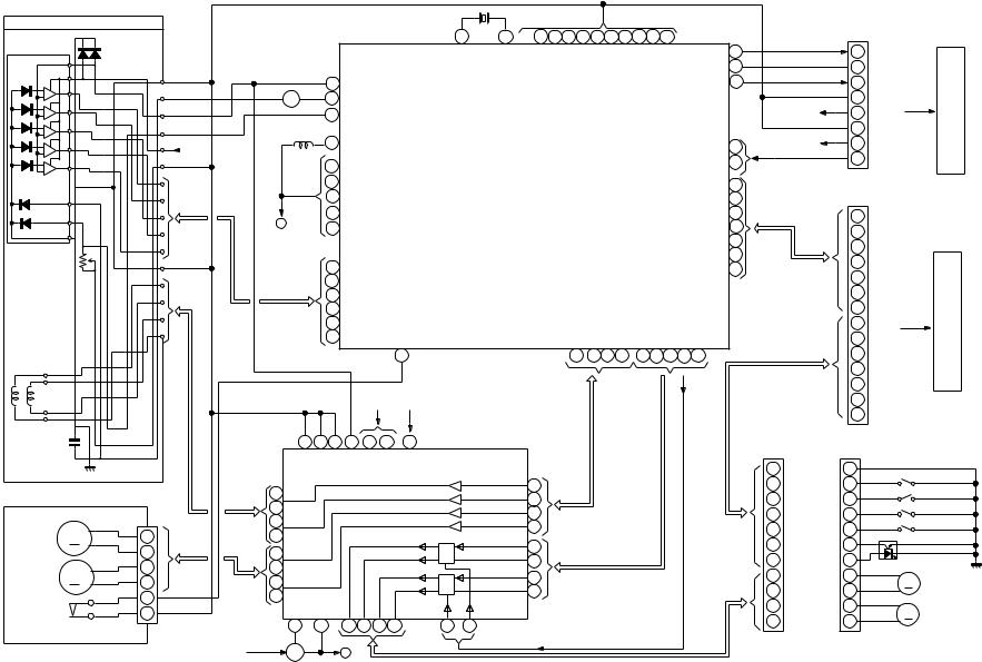
Figure 4-2 BLOCK DIAGRAM (2/3) |
|
|
|
|
|
|||||||||
4 – 2
|
|
PICKUP UNIT |
|
|
|
|
|
|
|
|
|
|
XL1 |
|
|
|
|
|
|
|
|
|
|
|
|
|
|
|
|
HP515-XL |
|
|
|
|
|
|
|
|
|
|
|
|
|
|
|
|
|
|
|
|
|
|
|
|
|
|
|
|
|
|
|||
|
|
|
|
|
|
|
|
|
|
|
|
|
16.9344 MHz 48 |
47 |
79 61 56 55 54 51 46 40 28 |
25 |
|
|
|
|
|
|
|
|
|
|
|||||
|
|
|
|
|
|
|
|
|
|
|
|
|
|
|
XIN |
XOUT |
|
|
|
|
|
|
RCHO |
44 |
|
1 |
R-CH |
|
|
TO |
|
|
|
|
VCC |
|
|
|
|
|
|
|
|
|
|
|
|
|
|
|
|
|
LRVSS |
43 |
|
2 |
AGND |
|
|
|
|||
|
|
|
|
|
|
|
|
|
|
|
|
|
|
|
|
|
|
|
|
|
|
|
|
|
|
|
|||||
|
|
|
|
|
|
|
|
|
|
|
|
|
|
|
|
|
|
|
|
|
|
LCHO |
42 |
|
|
L-CH |
|
|
MAIN |
|
|
|
|
|
VREF |
|
|
|
|
13 |
VREF |
|
|
|
|
|
|
|
|
|
|
|
|
|
3 |
|
|
|
|||||
|
|
|
|
|
|
|
|
|
|
|
|
|
|
|
|
|
|
|
|
|
|
|
|
||||||||
|
|
|
|
|
Q1 |
|
19 |
LDD |
|
|
|
|
|
|
|
|
|
|
|
|
|
|
|
|
4 |
DGND |
|
|
|
|
|
|
|
|
E |
|
|
|
|
|
|
|
|
|
|
|
|
|
|
|
|
|
|
|
|
|
SECTION |
|
|||||
|
|
|
|
|
|
|
49 |
XVDD |
|
|
|
|
|
|
|
|
|
|
|
|
LVDD |
41 |
+B4 |
7 |
+8V |
|
|
|
|||
|
|
|
A |
|
|
|
|
20 |
LDS |
|
|
|
|
|
|
|
|
|
|
|
|
|
|
|
+B8 |
5 |
D_+5V |
|
|
|
|
|
|
|
|
|
|
|
|
|
|
|
|
|
|
|
|
|
|
|
|
|
|
|
|
|
6 |
|
|
|
|
|
|
|
|
|
B |
|
|
0.82µH |
|
|
|
|
|
|
|
|
|
|
|
|
|
|
|
|
|
|
|
D_GND |
|
|
|
||
|
|
|
|
|
|
|
|
|
|
|
|
|
|
|
|
|
|
|
|
|
|
|
|
|
|
|
|
|
|
||
|
|
|
F |
|
+B8 |
|
|
|
|
|
|
|
|
|
|
IC1 |
|
|
|
|
|
|
RVDD |
+B7 |
|
8 |
A_+5V |
|
|
|
|
|
|
|
C |
|
|
|
|
1 |
AVDD1 |
|
|
|
|
|
LC78648E |
|
|
|
|
|
45 |
|
|
|
|
|
|||||
|
|
|
|
|
|
|
|
|
|
|
|
|
|
|
|
|
|
|
|
CNP2 |
|
|
|
|
|||||||
|
|
|
|
|
|
|
|
26 |
AVDD2 |
|
|
|
|
|
|
|
|
|
|
CE |
62 |
|
|
|
|
|
|||||
|
|
|
|
|
|
|
|
|
|
|
|
|
CD |
|
|
|
|
|
|
|
|
|
|
|
|
|
|||||
|
|
|
|
|
|
|
|
|
|
|
|
|
|
|
|
|
|
|
|
|
|
|
|
|
|
|
|
|
|||
|
|
|
|
|
|
|
|
27 |
DVDD |
|
|
|
|
|
|
|
|
|
|
|
CL |
63 |
|
CNP5 |
|
|
|
|
|||
|
|
|
|
|
|
|
|
|
|
|
DIGITAL SIGNAL PROCESSOR |
|
|
|
|
|
|
|
|
|
|||||||||||
|
|
|
|
|
A |
|
|
60 |
DVDD |
|
|
|
|
|
|
|
DI |
64 |
|
14 |
CD_RES |
|
|
|
|||||||
|
|
|
|
|
|
|
|
VVDD |
|
|
|
|
|
|
|
|
|
|
|
|
DO |
65 |
|
|
|
|
|||||
|
|
|
|
|
|
|
80 |
|
|
|
|
|
|
|
|
|
|
|
|
|
13 |
WRQ |
|
|
|
|
|||||
|
|
|
|
|
+5V |
|
|
|
|
|
|
|
|
|
|
|
|
|
|
|
|
|
|
||||||||
|
(3/3)DIAGRAMBLOCK3-4Figure |
|
|
|
|
|
|
|
|
|
|
|
|
|
|
|
|
|
|
|
*WRQ |
66 |
|
|
|
|
|
||||
3–4 |
TR– |
|
|
|
|
|
|
|
|
|
|
|
FOCUS/TRACKING/ |
|
|
|
SPEED |
|
|
12 |
DRF |
|
|
SECTIONDISPLAYFROM |
|
||||||
|
|
|
|
|
|
|
|
|
|
|
|
|
|
|
*RES 67 |
|
|
|
|
||||||||||||
|
|
|
|
|
|
|
|
|
|
|
|
|
|
|
|
|
|
|
|
|
|
|
|
|
|
|
|
||||
|
|
|
|
|
|
|
|
|
|
|
|
|
|
|
|
|
|
|
|
|
SPEED/CONT6MO |
|
|
11 |
DO |
|
|
|
|
||
|
|
|
|
|
|
|
|
7 |
AIN |
|
|
|
|
|
|
|
|
|
|
|
|
DRF 68 |
|
|
|
|
|
||||
|
|
|
|
|
|
|
|
|
|
|
|
|
|
|
|
|
|
|
A+/CONT5MOT |
|
10 |
DI |
|
|
|
|
|||||
|
|
|
|
|
|
|
|
8 |
CIN |
|
|
|
CONT1 |
|
|
|
FDO |
SLDO TDO |
SPDO |
B+/CONT3MO /CONT2-B MO |
/CONT4-A MOT |
|
|
|
|
|
|
||||
|
|
|
|
|
|
|
|
15 |
FIN |
|
|
|
|
|
|
|
|
6 |
CLAMP |
|
|
|
|
||||||||
|
|
|
|
|
|
|
|
9 |
BIN |
|
|
|
|
|
|
|
|
|
|
|
|
|
|
|
|
9 |
CL |
|
|
|
|
|
|
|
|
|
|
|
|
10 |
DIN |
|
|
|
|
|
|
|
|
|
|
|
|
|
|
|
|
8 |
CE |
|
|
|
|
|
|
|
|
|
|
|
|
14 |
EIN |
|
|
|
|
|
|
|
|
|
|
|
|
|
|
|
|
7 |
DISC |
|
|
|
|
|
|
|
TR– |
|
|
|
|
|
|
|
|
|
36 |
|
|
|
21 |
22 23 |
24 |
35 36 70 |
74 75 |
|
|
5 |
TRAY_SW1 |
|
|
||||
|
|
|
TR+ |
|
|
|
|
|
|
|
|
|
|
|
|
|
|
|
|
||||||||||||
|
|
TR+ |
|
|
|
|
|
|
|
|
|
|
|
|
|
|
|
|
|
|
|
|
|
|
4 |
TRAY_SW2 |
|
|
|||
|
|
|
|
|
|
|
|
|
|
|
|
|
|
|
|
|
|
|
|
|
|
|
|
|
|
|
|||||
|
|
FO+ |
FO+ |
|
|
|
|
|
|
|
|
|
|
|
|
IC2 |
|
|
|
|
|
|
|
|
|
3 |
PHOTO |
|
|
|
|
|
|
|
|
|
|
|
|
|
|
|
|
|
|
|
|
|
|
|
|
|
|
|
2 |
D_GND |
|
|
|
||||
|
|
FO– |
|
|
|
|
|
|
|
+B8 |
|
+B4 |
|
|
|
|
|
|
|
|
|
|
|
|
|
|
|||||
|
|
|
|
|
|
|
|
|
|
|
LA6261 |
|
|
|
|
|
|
|
|
|
|
|
|
||||||||
|
|
|
|
|
|
|
|
|
|
|
|
|
|
|
|
|
|
|
|
1 |
+5V |
|
|
|
|
||||||
|
|
|
|
|
|
|
|
|
|
|
|
|
|
|
|
|
|
|
|
|
|
|
|
|
|
|
|
||||
|
|
|
|
|
|
|
|
|
|
|
|
|
|
|
|
|
|
|
|
|
|
|
|
|
|
|
|
|
|
||
|
|
|
|
|
|
|
|
|
|
|
|
|
|
SPIN/SLED DRIVER |
|
|
|
_ |
|
|
|
|
|
|
|
|
|
|
|||
|
|
|
|
|
|
30 |
26 |
7 |
25 |
27 |
9 |
|
28 |
|
|
|
MO |
|
|
|
|
|
|
|
|
|
|
||||
|
|
|
|
|
|
|
|
|
|
|
|
|
|
|
|
|
|
|
|
|
|
|
|
||||||||
|
|
|
|
|
|
|
|
|
|
|
|
|
|
|
|
|
|
|
|
|
|
|
|
|
|||||||
|
|
|
GND |
|
|
PGND2 |
SGND |
PGND1 |
VREFIN |
SVCC |
PVCC1 |
|
PVCC2 |
|
|
VIN1 |
|
|
|
|
|
|
|
|
|
|
|
|
TRAY SW2 |
|
|
|
|
|
|
|
|
|
|
|
|
|
|
|
|
|
|
|
|
|
|
|
|
|
|
1 |
D_GND |
1 |
|
|
SW3 |
|
|
|
|
|
|
|
|
|
|
|
|
|
|
|
|
|
|
|
|
|
|
|
|
|
|
|
|
|
|
|
|||
|
|
|
|
|
1 |
VO3+ |
|
|
|
|
|
|
|
|
|
VIN2 |
11 |
|
|
|
|
|
|
2 |
TRAY_SW2 |
2 |
|
|
SW2 |
|
|
|
|
|
|
|
|
|
|
|
|
|
|
|
|
13 |
|
|
|
|
|
|
3 |
TRAY_SW1 |
3 |
|
|
|
|
||||
|
|
|
|
|
2 |
VO3– |
|
|
|
|
|
|
|
|
|
VIN3 |
|
|
|
|
|
|
SW1 |
|
TRAY SW1 |
|
|||||
|
|
|
|
|
|
|
|
|
|
|
|
|
|
15 |
|
|
|
|
|
|
4 |
CLAMP |
4 |
|
|
||||||
|
|
|
|
|
35 |
VO4+ |
|
|
|
|
|
|
|
|
|
VIN4 |
|
|
|
|
|
|
CLAMP |
|
|
|
|
||||
|
|
M1A |
+ |
|
|
|
|
|
|
|
|
|
|
17 |
|
|
|
|
|
|
5 |
5 |
|
SW4 |
|
|
|||||
|
|
|
|
VO4– |
|
|
|
|
|
|
|
|
|
|
|
|
|
|
|
|
DISC |
|
|
|
|
||||||
|
|
M |
6 |
36 |
|
|
|
|
|
|
|
|
|
FWD6 |
|
|
|
|
|
|
|
RX1 DISC |
|
||||||||
|
|
SPINDLE |
|
|
|
|
|
|
|
|
|
22 |
|
|
|
|
|
|
6 |
PHOTO |
6 |
|
|||||||||
|
|
MOTOR |
– |
5 |
3 |
VO2+ |
|
|
|
|
|
|
|
|
|
REV6 |
|
|
|
|
|
|
PHOTO |
|
|
||||||
|
|
|
|
|
|
|
|
|
|
|
|
|
23 |
|
|
|
|
|
|
7 |
+5V |
7 |
|
|
|||||||
|
|
M2A |
+ |
4 |
4 |
VO2– |
|
|
|
|
|
|
|
|
|
FWD5 |
|
|
|
|
|
|
|
|
|||||||
|
|
|
|
|
|
|
|
|
|
|
|
|
|
|
|
|
|
8 |
|
8 |
INTERRUPTER |
GND |
|||||||||
|
|
SLED |
M |
3 |
5 |
VO1+ |
|
|
|
|
|
|
|
|
|
REV5 19 |
|
|
|
|
|
|
TR+ |
+ |
M |
M1 |
|
||||
|
|
|
|
|
|
|
|
|
|
|
|
|
|
|
|
|
9 |
9 |
|
|
|||||||||||
|
|
MOTOR |
– |
2 |
6 |
VO1– |
|
|
VO5+ –VO5 |
–VO6 |
VO6+ |
|
|
|
|
20 |
|
|
|
|
|
|
CAM+ |
– |
|
TRAY |
|
||||
|
|
SW1A |
|
|
|
|
|
|
|
|
|
|
|
|
|
10 |
10 |
+ |
|
M2 |
|
||||||||||
|
|
|
|
|
|
|
|
|
|
|
|
|
|
|
|
|
|
|
|
|
TR– |
|
|
|
MOTOR |
|
|||||
|
|
PICKUP-IN |
|
1 |
|
|
|
|
|
|
|
|
VCONT6 |
|
VCONT5 |
|
|
|
|
|
|
|
11 |
CAM– |
11 |
– |
M |
MAIN CAM |
|||
|
|
|
|
|
CNP3 |
8 |
10 |
34 33 32 |
31 |
24 |
21 |
|
|
|
|
|
|
|
|
|
MOTOR |
|
|||||||||
|
|
|
|
|
|
|
|
|
|
|
|
|
|
|
|
|
|
|
|
|
|
|
|
|
|
|
|
|
|
|
|
|
|
|
|
|
+B8 |
Q2 |
|
|
A |
|
|
|
|
|
|
|
|
|
|
|
|
|
|
CNP4 |
CNB1 |
|
|
|
|
|
|
|
|
|
|
|
|
|
|
|
|
|
|
|
|
|
|
|
|
|
|
|
|
|
|
|
|
|
|
|
|||
|
|
|
|
|
|
|
|
+5V |
|
|
|
|
|
|
|
|
|
|
|
|
|
|
|
|
|
|
|
|
|
|
|

CHAPTER 5. CIRCUIT DESCRIPTION
[1] WAVEFORMS OF CD CIRCUIT
|
|
|
Stopped |
|
|
|
|
|
|
|
|
|
|
CH1=500 mV |
|
CH3=500 mV |
|
500 ms/div |
|||
|
|
|
DC |
10:1 |
|
DC 10:1 |
|
(500 ms/div) |
||
|
|
T |
|
|
|
|
|
|
|
NORM:20 kS/s |
|
|
|
|
|
|
|
|
|
|
|
1 |
IC1 21 |
|
FDO |
|
|
|
|
|
|
|
1 |
|
|
|
|
|
|
|
|
||
2 |
|
|
TDO |
|
|
|
|
|
|
|
IC1 22 |
3 |
|
|
|
|
|
|
|
|
|
|
|
|
|
|
|
|
|
|
||
|
|
|
|
|
|
|
|
|
|
CH1 |
|
|
|
|
|
|
|
|
|
|
v/DIV |
|
|
|
|
|
|
|
|
|
|
500 mV |
|
|
|
=Filter= |
|
=Offset= |
=Record Length= |
=Trigger= |
|||
|
|
Smoothing : |
ON |
CH1 : |
0.000 V |
Main : |
100 K |
Mode : AUTO |
||
|
|
BW |
: FULL |
|
CH2 : |
0.0 V |
Zoom : |
2 K |
Type : EDGE CH1 |
|
|
|
|
|
|
CH3 : |
0.000 V |
|
|
Delay : |
0.0 ns |
|
|
|
|
|
CH4 : |
0.00 V |
|
|
Hold off : |
0.2 µs |
|
|
|
Stopped |
|
|
|
|
|
|
|
|
|
|
CH1=500 mV |
CH2=10 V |
CH3=1 V |
|
500 ms/div |
|||
|
|
|
|
DC |
10:1 |
DC 10:1 |
DC |
10:1 |
|
(500 ms/div) |
|
|
|
|
|
|
|
|
|
|
NORM:20 kS/s |
1 |
IC1 21 |
1 |
FDO |
3 |
IC1 68 |
T |
DRF |
2 |
|||
|
|
||
4 |
IC1 17 |
|
TE |
3 |
|
|
|
|
|
|
|
|
|
|
|
|
CH2 |
|
|
|
|
|
|
|
|
|
|
|
Position |
|
CH Position To |
|
|
|
|
|
|
0.20 div |
|||
-3 div |
-1 div |
|
0 div |
|
+1 div |
|
+3 div |
|
|
|
|
=Filter= |
=Offset= |
=Record Length= |
|
=Trigger= |
|
|
|||||
Smoothing : |
ON CH1 : |
0.000 V |
Main : |
100 K |
Mode : AUTO |
|
|||||
BW : FULL |
CH2 : |
0.0 V |
Zoom : |
2 K |
Type : EDGE CH1 |
||||||
|
CH3 : |
0.00 V |
|
|
|
Delay : |
0.0 ns |
||||
|
CH4 : |
0.00 V |
|
|
|
Hold off : |
0.2 µs |
||||
5 |
IC1 |
4 |
|
|
Vp-p=1.0 V~1.3 V |
|
|
0.5 mV/div,0.5 µsec/div |
4
3
IC1 17
IC1 68
Stopped |
T |
|
|
|
|
CH1=10 V |
CH2=1 V |
100 ms/div |
DC 10:1 |
DC 10:1 |
(100 ms/div) |
|
|
NORM:100 kS/s |
TE
2 

T |
DRF |
1 |
|
=Filter= |
=Offset= |
=Record Length= |
=Trigger= |
||||
Smoothing : ON |
CH1 : |
0.0 V |
Main : |
100 K |
Mode : NORMAL |
||
BW : FULL |
CH2 : |
0.00 V |
Zoom : |
2 K |
Type : EDGE CH1 |
||
|
CH3 |
: |
0.00 V |
|
|
Delay : |
2.924 ms |
|
CH4 |
: |
0.00 V |
|
|
Hold off : |
0.2 µs |
|
|
|
|
|
|
|
|
|
|
|
|
XL-HP515 |
||
|
|
|
Stopped |
|
|
|
T |
|
|
|
|
1999/04/07 09:51:15 |
||
|
|
|
|
|
|
|
|
|
|
|
||||
|
|
|
CH1=200 mV |
CH2=500 mV |
|
|
|
|
|
500 ms/div |
||||
|
|
|
DC |
10:1 |
|
DC 10:1 |
|
|
|
|
|
(500 ms/div) |
||
|
|
|
|
|
|
|
|
|
|
|
|
|
NORM:20 kS/s |
|
|
|
|
T |
|
|
|
|
|
|
|
|
|
|
|
1 |
IC1 21 |
|
2 |
|
|
|
|
|
|
|
|
|
|
|
|
|
|
|
|
|
|
|
|
|
|
|
|
||
6 |
IC1 24 |
|
1 |
|
|
|
|
|
|
|
|
|
|
|
|
|
|
|
|
|
|
|
|
|
|
|
|
||
|
|
|
=Filter= |
|
|
=Offset= |
=Record Length= |
|
|
=Trigger= |
||||
|
|
Smoothing : |
ON |
CH1 : |
0.000 V |
Main : |
|
100 K |
|
Mode : NORMAL |
||||
|
|
BW : FULL |
|
CH2 : |
0.000 V |
Zoom : |
2 K |
Type |
: EDGE CH2 |
|||||
|
|
|
|
|
CH3 : |
0.00 V |
|
|
|
|
Delay : |
2.924 ms |
||
|
|
|
|
|
CH4 : |
0.00 V |
|
|
|
|
Hold off : |
0.2 µs |
||
|
|
|
Stopped |
|
|
|
|
|
|
|
|
1999/04/05 |
17:33:17 |
|
|
|
|
CH1=500 mV |
|
|
|
CH3=1 V |
|
CH4=1 V |
500 ms/div |
||||
|
|
|
DC 10:1 |
|
|
|
DC 10:1 |
|
DC |
10:1 |
(500 ms/div) |
|||
|
|
|
|
|
|
|
|
|
|
|
|
|
NORM:20 kS/s |
|
7 |
IC1 76 |
3 |
|
|
|
|
|
|
|
|
|
|
|
|
|
|
|
|
|
|
|
|
|
|
|
|
|
||
|
|
4 |
|
|
|
|
|
|
|
|
|
|
|
|
8 |
IC1 77 |
|
PDO2 |
|
|
|
|
|
|
|
|
|
|
|
|
|
|
|
|
|
|
|
|
|
|
|
|
||
|
|
T |
|
|
|
|
|
|
|
|
|
|
|
|
1 |
IC1 21 |
1 |
|
|
|
|
|
|
|
|
|
|
|
CH1 |
|
|
|
|
|
|
|
|
|
|
|
|
|
|
|
|
|
|
|
|
|
|
|
|
|
|
|
|
|
v/DIV |
|
|
|
|
|
|
|
|
|
|
|
|
|
|
500 mV |
|
|
|
=Filter= |
|
=Offset= |
=Record Length= |
|
=Trigger= |
||||||
|
|
Smoothing : ON |
CH1 : |
|
0.000 V |
Main : |
100 K |
Mode : AUTO |
|
|||||
|
|
BW |
: FULL |
CH2 : |
|
0.0 V |
Zoom : |
|
2 K |
Type : EDGE CH2 |
||||
|
|
|
|
CH3 : |
|
0.00 V |
|
|
|
Delay : |
|
0.0 ns |
||
|
|
|
|
CH4 : |
|
0.00 V |
|
|
|
Hold off : |
|
0.2 µs |
||
|
|
|
Stopped |
T |
|
|
|
|
|
|
|
1999/04/07 |
09:25:28 |
|
|
|
|
|
|
|
|
|
|
|
|
||||
|
|
|
CH1=2 V |
|
|
|
|
|
|
|
|
500 ns/div |
||
|
|
|
DC 10:1 |
|
|
|
|
|
|
|
|
(500 ns/div) |
||
|
|
|
|
|
|
|
|
|
|
|
|
|
NORM:200 MS/s |
|
|
|
|
T |
|
|
|
|
|
|
|
|
9 |
IC1 39 |
1 |
DOUT |
|
|
|
|
|
|
|
|
|
|
|
|
|
|
|
|
||||
|
|
|
|
=Filter= |
|
=Offset= |
=Record Length= |
=Trigger= |
|||
|
|
|
Smoothing : ON |
CH1 : |
0.00 V |
Main : |
1 K |
Mode : NORMAL |
|||
|
|
|
BW |
: FULL |
|
CH2 : |
0.00 V |
Zoom : |
100 |
Type : EDGE CH1 |
|
|
|
|
|
|
|
CH3 : |
0.00 V |
|
|
Delay : |
2.887 ms |
|
|
|
|
|
|
CH4 : |
0.00 V |
|
|
Hold off : |
0.2 µs |
|
|
|
Stopped |
|
T |
|
|
|
1999/04/05 |
20:50:17 |
|
|
|
|
|
|
|
|
|
||||
|
|
|
|
CH1=2 V |
CH2=2 V |
CH3=2 V |
|
5 µs/div |
|||
|
|
|
|
DC |
10:1 |
DC |
10:1 |
DC 10:1 |
|
(5 µs/div) |
|
|
|
|
|
|
|
|
|
|
|
NORM:100 kS/s |
|
10 IC1 |
57 |
|
|
|
|
|
|
|
|
|
|
|
|
|
1 |
LRSY |
|
|
|
|
|
|
|
|
|
|
|
|
|
|
|
|
|
|
|
11 IC1 58 |
|
|
|
|
|
|
|
|
|
||
|
|
|
2 |
DATACK |
|
|
|
|
|
|
|
|
|
|
|
|
|
|
|
|
|
|
|
12 |
IC1 59 |
T |
|
|
|
|
|
|
|
|
|
|
|
|
|
|
|
|
|
|
|||
|
|
|
3 |
|
|
|
|
|
|
|
|
|
|
|
|
DATA |
|
|
|
|
|
|
CH3 |
|
|
|
|
|
|
|
|
|
|
|
v/DIV |
|
|
|
|
|
|
|
|
|
|
|
2 V |
|
|
|
|
=Filter= |
|
=Offset= |
=Record Length= |
=Trigger= |
|||
|
|
|
Smoothing : ON |
CH1 : |
0.00 V |
Main : |
5 K |
Mode : AUTO |
|
||
|
|
|
BW |
: FULL |
|
CH2 : |
0.00 V |
Zoom : |
100 |
Type : EDGE CH3 |
|
|
|
|
|
|
|
CH3 : |
0.00 V |
|
|
Delay : |
0.0 ns |
|
|
|
|
|
|
CH4 : |
0.00 V |
|
|
Hold off : |
0.2 µs |
5 – 1
XL-HP515
[2] VOLTAGE
|
IC1 |
PIN |
VOLTAGE |
NO. |
|
1 |
3.20 V |
2 |
1.61V |
3 |
1.61 V |
4 |
1.60 V |
5 |
1.61 V |
6 |
3.06 V |
7 |
1.65 V |
8 |
1.65 V |
9 |
1.65 V |
10 |
1.65 V |
11 |
1.48 V |
12 |
0 V |
13 |
1.65 V |
14 |
0 V |
15 |
1.65 V |
16 |
1.47 V |
17 |
1.48 V |
18 |
0 V |
19 |
0 V |
20 |
0 V |
21 |
1.60 V |
22 |
0 V |
23 |
1.61 V |
24 |
1.61 V |
25 |
0 V |
26 |
0 V |
27 |
3.20 V |
28 |
0 V |
29 |
3.20 V |
30 |
0 V |
31 |
0 V |
32 |
1.59 V |
33 |
1.60 V |
34 |
3.20 V |
35 |
0 V |
36 |
0 V |
37 |
0 V |
38 |
0 V |
39 |
0 V |
40 |
0 V |
41 |
3.61 V |
42 |
0 V |
43 |
0 V |
44 |
1.80 V |
45 |
3.60 V |
46 |
0 V |
47 |
1.45 V |
48 |
1.49 V |
49 |
3.19 V |
50 |
3.79 V |
51 |
0 V |
52 |
0 V |
53 |
0 V |
54 |
0 V |
55 |
0 V |
56 |
0 V |
57 |
0 V |
58 |
0 V |
59 |
0 V |
60 |
3.20 V |
61 |
0 V |
62 |
0 V |
63 |
0.63 V |
64 |
0 V |
65 |
5.16 V |
66 |
5.18 V |
67 |
4.68 V |
68 |
0 V |
69 |
0 V |
70 |
0 V |
71 |
0 V |
72 |
0 V |
73 |
0 V |
74 |
4.86 V |
75 |
4.86 V |
76 |
3.01 V |
77 |
0 V |
78 |
1.12 V |
79 |
0 V |
80 |
3.20 V |
|
IC2 |
PIN |
VOLTAGE |
NO. |
|
1 |
2.10 V |
2 |
2.20 V |
3 |
2.10 V |
4 |
2.20 V |
5 |
2.10 V |
6 |
2.20 V |
7 |
0 V |
8 |
4.37 V |
9 |
5.02 V |
10 |
3.20 V |
11 |
1.62 V |
12 |
1.65 V |
13 |
1.62 V |
14 |
1.65 V |
15 |
1.62 V |
16 |
0 V |
17 |
1.62 V |
18 |
1.64 V |
19 |
4.71 V |
20 |
4.71 V |
21 |
3.92 V |
22 |
3.11 V |
23 |
3.10 V |
24 |
2.50 V |
25 |
1.65 V |
26 |
0 V |
27 |
5.02 V |
28 |
8.68 V |
29 |
5.02 V |
30 |
0.59 V |
31 |
0.71 V |
32 |
0 V |
33 |
0 V |
34 |
0 V |
35 |
2.11 V |
36 |
2.20 V |
|
|
|
IC101 |
PIN |
VOLTAGE |
NO. |
|
1 |
0 V |
2 |
0 V |
3 |
0.57 V |
4 |
2.03 V |
5 |
0.44 V |
6 |
0 V |
7 |
0 V |
8 |
0.58 V |
9 |
3.45 V |
10 |
3.35 V |
11 |
0 V |
12 |
0 V |
13 |
6.97 V |
14 |
4.16 V |
15 |
0 V |
16 |
3.42 V |
17 |
0.57 V |
18 |
0 V |
19 |
0 V |
20 |
0.41 V |
21 |
2.03 V |
22 |
0.57 V |
23 |
0 V |
24 |
0 V |
Q1
PINNO. VOLTAGE
E 3.2 V
C 94.3 mV
B 3.2 V
Q2
PINNO. VOLTAGE
E 4.9 V
C 3.2 V
B 4.2 V
Q110
PINNO. VOLTAGE
1-0.0 mV
29.9 V
315.1 V
|
IC301 |
PIN |
VOLTAGE |
NO. |
|
1 |
0 V |
2 |
0 V |
3 |
0.29 V |
4 |
0.20 V |
5 |
0 V |
6 |
0.29 V |
7 |
0.26 V |
8 |
0.29 V |
9 |
0.29 V |
|
|
|
|
|
IC302 |
PIN |
VOLTAGE |
NO. |
12.57 V
20 V
30 V
40 V
50 V
65.22 V
710.18 V
84.75 V
90 V
100 V
115.23 V
120 V
135.23 V
140 V
150 V
162.59 V
175.24 V
180 V
190 V
2010.18 V
210 V
222.57 V
IC303
PINNO. VOLTAGE
11.97 V
25.15 V
31.97 V
41.98 V
50 V
60 V
75.21 V
83.59 V
95.15 V
10 0 V
11 2.01 V
12 1.25 V
13 2.27 V
14 1.13 V
15 1.10 V
16 1.95 V
17 0 V
18 1.29 V
19 2.08 V
20 1.29 V
21 1.95 V
22 1.95 V
23 5.15 V
24 3.65 V
|
Q302 |
PIN |
VOLTAGE |
NO. |
|
E |
2.1 V |
C |
0 V |
B |
0 V |
|
|
|
Q360 |
PIN |
VOLTAGE |
NO. |
|
E |
16.01 V |
C |
0.4 mV |
B |
10.01 mV |
|
|
|
Q601 |
PIN |
VOLTAGE |
NO. |
|
E |
0.3 mV |
C |
0.2 mV |
B |
0.3 V |
|
IC601 |
|
|
IC701 |
|
|
PIN |
VOLTAGE |
|
PIN |
VOLTAGE |
PIN |
VOLTAGE |
NO. |
|
NO. |
NO. |
|||
1 |
0 V |
|
1 |
4.74 V |
51 |
0 V |
2 |
0 V |
|
2 |
4.65 V |
52 |
0 V |
3 |
0 V |
|
3 |
0 V |
53 |
0 V |
4 |
5.10 V |
|
4 |
4.70 V |
54 |
0 V |
5 |
5.10 V |
|
5 |
4.72 V |
55 |
5.17 V |
6 |
5.10 V |
|
6 |
4.72 V |
56 |
5.17 V |
7 |
5.10 V |
|
7 |
0 V |
57 |
-29.70 V |
8 |
5.11 V |
|
8 |
0 V |
58 |
0 V |
9 |
5.10 V |
|
9 |
0 V |
59 |
-0.26 V |
10 |
5.10 V |
|
10 |
4.83 V |
60 |
-0.24 V |
11 |
5.10 V |
|
11 |
2.27 V |
61 |
-0.22 V |
12 |
5.10 V |
|
12 |
1.99 V |
62 |
-0.20 V |
13 |
5.10 V |
|
13 |
0 V |
63 |
-0.19 V |
14 |
5.10 V |
|
14 |
4.73 V |
64 |
-0.19 V |
15 |
5.10 V |
|
15 |
0 V |
65 |
-0.18 V |
16 |
5.10 V |
|
16 |
4.74 V |
66 |
-0.17 V |
17 |
5.10 V |
|
17 |
0 V |
67 |
-0.16 V |
18 |
5.10 V |
|
18 |
0 V |
68 |
0 V |
19 |
5.10 V |
|
19 |
5.22 V |
69 |
-29.90 V |
20 |
5.10 V |
|
20 |
0 V |
70 |
-29.90 V |
21 |
5.10 V |
|
21 |
0 V |
71 |
-29.90 V |
22 |
5.10 V |
|
22 |
4.88 V |
72 |
-29.90 V |
23 |
10.20 V |
|
23 |
0 V |
73 |
-29.90 V |
24 |
0 V |
|
24 |
0 V |
74 |
-19.76 V |
|
|
|
25 |
0 V |
75 |
-27.40 V |
|
|
|
26 |
5.20 V |
76 |
-24.87 V |
|
IC901 |
|
27 |
0 V |
77 |
-22.29 V |
PIN |
VOLTAGE |
|
28 |
5.01 V |
78 |
-22.30 V |
NO. |
|
|
29 |
5.01 V |
79 |
-30.13 V |
1 |
46.70 V |
|
||||
|
30 |
2.64 V |
80 |
-27.43 V |
||
2 |
22.90 V |
|
||||
|
31 |
5.01 V |
81 |
-14.60 V |
||
3 |
10.80 V |
|
||||
|
32 |
5.01V |
82 |
-27.20 V |
||
4 |
-10.90 V |
|
||||
|
33 |
0 V |
83 |
-19.30 V |
||
5 |
-22.90 V |
|
||||
|
34 |
0 V |
84 |
-6.08 V |
||
6 |
-48.80 V |
|
||||
|
35 |
5.01 V |
85 |
-21.85 V |
||
7 |
0 V |
|
||||
|
36 |
1.67 V |
86 |
-27.22 V |
||
8 |
0 V |
|
||||
|
37 |
5.20 V |
87 |
-21.89 V |
||
9 |
0 V |
|
||||
|
38 |
5.01 V |
88 |
-17.00 V |
||
10 |
0 V |
|
||||
|
39 |
4.87 V |
89 |
-27.38 V |
||
11 |
0 V |
|
||||
|
40 |
0 V |
90 |
-27.10 V |
||
12 |
-47.40 V |
|
||||
|
41 |
2.02 V |
91 |
-27.07 V |
||
13 |
47.50 V |
|
||||
|
42 |
0 V |
92 |
-27.00V |
||
14 |
-0.16 V |
|
||||
|
43 |
13.10 V |
93 |
-27.00 V |
||
15 |
-0.16 V |
|
||||
|
44 |
0 V |
94 |
-27.35 V |
||
16 |
-46.30 V |
|
||||
|
45 |
0 V |
95 |
-27.27 V |
||
17 |
-0.17 V |
|
||||
|
46 |
4.74 V |
96 |
-27.11 V |
||
18 |
-0.16 V |
|
||||
|
47 |
0 V |
97 |
-27.00 V |
||
|
|
|
||||
|
|
|
48 |
4.61 V |
98 |
-27.07 V |
|
|
|
49 |
0 V |
99 |
-27.00 V |
|
|
|
50 |
0 V |
100 |
-26.83 V |
Q602
PINNO. VOLTAGE
E 0.3 mV
C 0.2 mV
B 0.7 V
Q603
PINNO. VOLTAGE
E 0.4 mV
C 0.2 mV
B 0.7 mV
Q604
PINNO. VOLTAGE
E 0.4 mV
C 0.1 mV
B 0.7 V
Q701
PINNO. VOLTAGE
E 12.9 V
C 0.8 mV
B 12.9 V
Q702
PINNO. VOLTAGE
E 15.9 V
C 10.0 mV
B 12.9 V
Q703
PINNO. VOLTAGE
10.9 mV
24.5 V
30.9 mV
Q711
PINNO. VOLTAGE
110.01 V
29.7 V
3207.2 mV
Q712
PINNO. VOLTAGE
E -392.1 mV
C 4.9 V
B 392.4 mV
Q713
PINNO. VOLTAGE
E 12.9 V
C 362.5 mV
B 12.9 V
Q714
PINNO. VOLTAGE
E 9.8 mV
C 4.5 V
B 9.9 mV
Q715
PINNO. VOLTAGE
E 12.9 V
C 9.8 mV
B 12.9 V
Q719
PINNO. VOLTAGE
19.9 mV
25.10 V
39.8 mV
Q841
PINNO. VOLTAGE
E 24.1 mV
C 126.0 mV
B 0.8 V
Q901
PINNO. VOLTAGE
E -0.18 mV
C -0.18 mV
B 0.5 V
Q902
PINNO. VOLTAGE
E 0.16 mV
C 0.5 V
B 0.16 mV
Q903
PINNO. VOLTAGE
E 0.7 mV
C 0.5 V
B -0.10 mV
Q904
PINNO. VOLTAGE
E 0.6 mV
C 0.5 V
B -0.9 mV
IC851
PINNO. VOLTAGE
15.22 V
213.11 V
320.66 V
40 V
519.72 V
610.22 V
78.67 V
IC854
PINNO. VOLTAGE
15.66 V
20.61 V
39.33 V
Q801
PINNO. VOLTAGE
E -29.12 V
C -29.77 V
B -42.4 V
Q908
PINNO. VOLTAGE
E 0.6 mV
C 0.5 V
B 0.8 mV
5 – 2
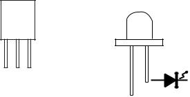
XL-HP515
CHAPTER 6. CIRCUIT SCHEMATICS AND PARTS LAYOUT
[1] NOTES ON SCHEMATIC DIAGRAM
•Resistor:
To differentiate the units of resistors, such symbol as K and M are used: the symbol K means 1000 ohm and the symbol M means 1000 kohm and the resistor without any symbol is ohm-type resistor. Besides, the one with “Fusible” is a fuse type.
•Capacitor:
To indicate the unit of capacitor, a symbol P is used: this symbol P means pico-farad and the unit of the capacitor without such a symbol is microfarad. As to electrolytic capacitor, the expression “capacitance/withstand voltage” is used.
(CH), (TH), (RH), (UJ): Temperature compensation (ML): Mylar type
(P.P.): Polypropylene type
•Schematic diagram and Wiring Side of P.W.Board for this model are subject to change for improvement without prior notice.
REF. NO |
DESCRIPTION |
POSITION |
SW1 |
CLAMP |
ON—OFF |
SW1A |
PICKUP IN |
ON—OFF |
SW2 |
TRAY SW1 |
ON—OFF |
SW3 |
TRAY SW2 |
ON—OFF |
SW4 |
DISC |
ON—OFF |
SW701 |
ON/STAND-BY |
ON—OFF |
SW702 |
CLOCK/TIMER |
ON—OFF |
SW703 |
REVERSE MODE |
ON—OFF |
SW704 |
REVERSE PLAY |
ON—OFF |
SW705 |
PRESET DOWN |
ON—OFF |
SW709 |
CD |
ON—OFF |
SW710 |
TUNER (BAND) |
ON—OFF |
SW711 |
VIDEO/AUX |
ON—OFF |
SW712 |
TAPE |
ON—OFF |
SW713 |
REC/PAUSE |
ON—OFF |
•The indicated voltage in each section is the one measured by Digital Multimeter between such a section and the chassis with no signal given.
1.In the tuner section, indicates AM indicates FM stereo
2.In the main section, a tape is being played back.
3.In the deck section, a tape is being played back.
4.In the power section, a tape is being played back.
5.In the CD section, the CD is stopped.
•Parts marked with “  ” (
” ( 


 ) are important for maintaining the safety of the set. Be sure to replace these parts with specified ones for maintaining the safety and performance of the set.
REF. NO |
DESCRIPTION |
POSITION |
SW714 |
TUNING/TIME UP |
ON—OFF |
SW715 |
TUNING/TIME DOWN |
ON—OFF |
SW716 |
STOP |
ON—OFF |
SW717 |
PLAY |
ON—OFF |
SW718 |
PRESET UP |
ON—OFF |
SW719 |
X-BASS/DEMO |
ON—OFF |
SW720 |
EQUALIZER |
ON—OFF |
SW721 |
MEMORY/SET |
ON—OFF |
SW722 |
DIRECT PLAY |
ON—OFF |
SW723 |
DISC 1 |
ON—OFF |
SW724 |
DISC 2 |
ON—OFF |
SW725 |
DISC 3 |
ON—OFF |
SW726 |
DISC 4 |
ON—OFF |
SW727 |
DISC 5 |
ON—OFF |
SW728 |
OPEN/CLOSE |
ON—OFF |
[2] TYPES OF TRANSISTOR AND LED
FRONT
VIEW
E |
C B |
(S) (G) (D) |
|
(1) |
(2) (3) |
KRC102 S |
KTA1504 GR |
KRC104 S |
KTC3199 GR |
KRA107 S |
KTC3200 GR |
KTA1504 Y |
KTC3875 GR |
KTA1271 Y |
KTC3203 Y |
KTA1273 Y |
KTC3194 Y |
KTA1274 Y |
KRA102 S |
FRONT
VIEW
SVC347S
SVC230C
6 – 1
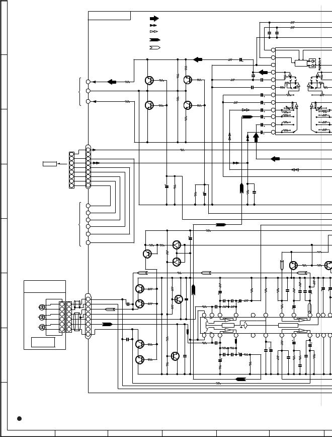
XL-HP515
[3] WIRING SIDE OF PWB/SCHEMATIC DIAGRAM
|
|
|
|
|
|
MAIN PWB-A1(1/2) |
|
|
|
FM SIGNAL |
|
|
|
|
|
|
|
|
|
|
|
|
|
|
|
|
|
|
|
|
|
|
|
|
|
|
|
|
|
|
||||
|
|
|
|
|
|
|
|
|
|
|
|
|
|
|
|
|
|
|
|
|
|
|
|
|
|
|
R601 |
1K |
|
|
|
|
|
|
|
|
|
|
|
|||||
A |
|
|
|
|
|
|
|
|
|
|
CD SIGNAL |
|
|
|
|
|
|
|
|
|
|
|
|
|
|
|
|
R602 |
1K |
|
|
|
|
|
|
|
|
|
|
|
||||
|
|
|
|
|
|
|
|
|
|
AUX SIGNAL |
|
|
|
|
|
|
|
|
|
|
C652 |
220P |
|
C651 |
220P |
|
|
IC601 |
|
|
|
|
|
|
|
|||||||||
|
|
|
|
|
|
|
|
|
|
|
|
|
|
|
|
|
|
|
|
|
|
|
|
|
|
|
|
|
|
|
||||||||||||||
|
|
|
|
|
|
|
|
|
|
|
PLAYBACK SIGNAL |
|
|
|
|
|
|
|
|
|
|
|
|
|
|
|
LC75341 |
|
|
|
|
|
|
|
||||||||||
|
|
|
|
|
|
|
|
|
|
|
RECORD SIGNAL |
|
|
|
|
|
|
|
|
|
|
|
|
|
AUDIO PROCESSOR |
|
||||||||||||||||||
|
|
|
|
|
|
|
|
|
|
|
|
|
|
|
|
|
|
|
|
|
1 |
|
|
|
|
|
|
|
|
|
|
|
|
|
|
|
|
|||||||
|
|
|
|
|
|
|
|
|
|
|
|
|
|
|
|
|
|
|
|
|
|
|
|
|
|
|
|
DI |
|
|
|
|
|
|
|
|
|
|
|
|
|
CL |
||
|
|
|
|
|
|
|
|
|
|
|
|
|
|
|
|
|
|
|
|
R605 |
C609 |
|
|
|
2 |
CE |
|
|
|
|
|
|
|
|
|
|
|
|
|
VD |
||||
|
|
|
|
|
|
|
|
|
|
|
|
|
|
|
|
|
|
|
|
|
|
|
|
|
|
|
|
|
|
|
|
|
|
|
|
|
– |
|
|
|
|
|
|
|
|
|
|
|
|
|
|
|
|
|
|
|
|
|
|
|
|
|
|
|
|
|
|
|
|
|
|
|
|
|
|
|
|
|
|
|
|
|
|
|
|
|
|
|
|
|
|
|
|
|
|
|
|
|
|
|
|
|
|
|
|
|
|
|
|
10K |
1/50 |
|
|
|
|
VSS |
|
|
|
CCB |
|
+ |
|
|
|
|
|
VRE |
||||||
|
|
|
|
|
|
|
|
|
|
|
|
|
|
|
|
|
|
|
|
|
|
|
3 |
|
|
|
|
+ |
|
|
|
|
|
|||||||||||
|
|
|
|
|
|
|
|
|
|
|
|
|
|
|
|
R613 |
|
|
|
|
|
|
|
|
|
|
|
|
INTERFACE |
|
|
|
|
|
|
|
||||||||
|
|
|
|
|
|
|
|
|
|
|
|
|
|
|
|
|
|
|
|
|
|
|
|
|
|
|
|
|
|
|
|
|
|
|
– |
|
|
|
|
|
|
|
||
|
|
|
|
|
|
|
|
|
|
|
|
|
|
|
|
390 |
|
|
|
|
|
|
|
|
|
|
|
|
LOUT |
|
|
|
|
|
|
|
|
|
|
|
ROU |
|||
|
|
|
|
|
|
|
|
|
Q603 KTC3875 GR |
|
|
R614 R615 2.2K 2.2K |
|
KTC3875 GR KTC3875 GR |
|
|
R611 |
|
|
|
R607 |
|
|
C607 |
|
|
4 |
– |
|
|
|
|
|
|
+ – |
|
|
|||||||
|
|
|
|
|
|
|
|
|
|
R617 |
|
|
|
|
|
|
|
|
|
|
|
|
|
|
|
|
|
|
|
|
|
|
|
|
||||||||||
|
|
|
TO MAINPWB(2/2) |
|
|
|
R619 |
|
|
|
|
|
2.2K |
|
|
|
3.3K |
|
|
0.15 |
|
|
|
|
|
|
+ |
|
|
|
|
|
|
|
|
|
|
|||||||
|
|
|
|
|
|
|
|
2.2K |
|
|
|
|
|
|
|
|
|
|
|
|
|
LBASS |
|
|
|
|
|
|
|
|
RBAS |
|||||||||||||
B |
|
|
|
1 |
L-CH |
330 |
|
|
Q602 Q601 |
|
|
|
|
|
|
|
|
|
|
|
C605 |
5 |
|
|
|
|
|
|
|
|
||||||||||||||
|
|
|
|
|
|
|
|
|
|
|
|
|
|
|
|
|
|
|
|
|
|
|
|
|
|
|
|
|
|
|
|
|
||||||||||||
|
|
|
|
|
|
|
|
|
|
|
|
|
|
|
|
|
|
C611 |
0.15 |
6 |
LTRE |
– |
|
|
|
|
|
|
RTR |
|||||||||||||||
|
|
|
|
|
A_GND |
|
|
|
|
|
|
|
|
|
|
|
|
0.0022 |
|
|
|
|
|
|
|
|
|
|
|
|
|
|
|
|||||||||||
|
|
|
|
2 |
|
|
|
|
|
|
|
|
|
|
|
|
|
|
|
|
|
|
|
|
|
|
|
|
|
|
|
|
||||||||||||
|
|
|
|
|
|
|
|
|
|
|
|
|
|
|
|
|
|
|
|
C613 |
1/50 |
|
LIN |
|
|
|
|
|
|
|
|
|
|
RI |
||||||||||
|
|
|
|
|
|
R618 |
|
|
|
|
|
|
|
|
|
R05 |
|
|
|
7 |
|
|
|
|
|
|
|
|
|
|
||||||||||||||
|
|
|
|
|
|
|
|
|
|
|
|
|
|
|
|
|
|
|
|
|
|
|
|
|
|
|
|
|
|
|
|
|
|
|||||||||||
|
|
|
|
|
|
330 |
|
|
|
|
|
|
|
|
|
|
|
|
|
|
|
|
|
|
|
|
|
|
|
|
|
|
|
|
||||||||||
|
|
|
|
3 |
R-CH |
|
|
|
|
|
|
|
|
|
0 |
|
|
|
|
C615 |
|
|
LSEL0 |
|
|
|
|
|
|
|
|
RSEL |
||||||||||||
|
|
|
|
|
|
|
|
|
|
|
|
|
|
|
|
|
|
|
8 |
|
|
|
|
|
|
|
|
|||||||||||||||||
|
|
|
|
|
|
|
|
|
|
|
|
|
|
|
|
|
|
|
|
|
|
|
|
|
|
|
|
|
||||||||||||||||
|
|
|
|
|
|
|
|
|
|
|
|
|
|
|
|
|
|
|
|
|
4.7/50 |
|
|
|
|
|
– |
|
|
|
|
|
|
|
|
|
||||||||
|
|
|
D146-- |
|
|
|
|
GR |
R616 |
|
|
R610 |
|
|
|
|
|
|
|
|
C617 |
1/50 |
|
L4 |
|
+ + |
AUX |
|
|
|
|
|
R |
|||||||||||
|
|
|
|
|
|
|
|
|
|
|
|
|
|
|
|
|
|
|
|
|
|
|
|
|
|
|
|
|
|
|
||||||||||||||
|
|
|
|
|
|
|
2.2K |
|
|
2.2K |
|
|
|
|
|
|
|
|
|
|
9 |
|
|
|
|
+ – + – |
|
|
|
|
|
|||||||||||||
|
|
|
|
|
|
|
|
|
|
Q604 KTC3875 |
|
|
|
|
|
R612 390 |
|
|
|
|
|
|
|
|
|
C619 |
1/50 |
10 L3 |
|
|
|
|
DECK |
|
|
|
|
|
|
|
R |
|||
|
|
|
|
|
|
|
|
|
|
|
|
|
|
|
|
|
|
|
|
|
|
|
|
C621 |
1/50 |
11 |
L2 |
|
|
|
TUNER |
|
|
|
|
|
|
|
R |
|||||
|
|
|
|
|
|
|
|
|
|
|
|
|
|
|
|
|
|
|
|
|
|
|
|
|
|
|
|
12 L1 |
|
|
|
|
CD |
|
|
|
|
|
|
|
R |
|||
C |
|
|
|
|
|
|
|
|
|
|
|
|
|
|
|
|
|
|
|
|
|
|
|
|
|
C623 |
|
|
|
|
|
|
|
|
|
|
|
|
|
|
|
|
|
|
|
|
|
|
|
|
|
|
|
|
|
|
|
|
|
|
|
|
|
|
|
|
|
|
|
1/50 |
|
|
|
|
|
|
|
|
|
|
|
|
|
|
|
|
|
||
|
|
|
|
|
|
BI601 |
|
|
|
|
|
|
R645 |
|
|
|
|
|
|
|
|
|
|
|
|
|
|
|
|
|
|
|
|
|
|
|
|
|
|
|
|
|
|
|
|
|
|
|
|
|
|
|
|
|
|
|
|
|
|
|
|
|
|
|
|
|
|
|
|
|
|
|
|
|
|
|
|
|
|
|
|
|
|
|
|
|
|
||
|
|
|
CNS2 R-CH |
1 |
|
|
|
|
|
|
|
|
0 |
|
|
|
|
|
|
|
|
|
|
|
|
|
|
|
|
|
|
|
|
|
|
|
|
|
|
|
|
|
|
|
|
|
|
|
|
|
|
|
|
|
|
|
|
|
|
|
|
|
|
|
|
|
|
|
|
|
|
|
|
|
|
|
|
|
|
|
|
|
|
|
|
|
|||
|
|
|
1 |
A_GND |
2 |
|
|
|
|
|
|
|
|
|
|
|
|
|
|
|
|
|
|
|
|
|
|
|
|
|
|
|
|
|
|
|
|
|
|
|
|
|
|
|
|
6-11 11 - E |
|
2 |
3 |
|
|
|
|
|
|
|
|
|
|
|
|
|
|
|
|
|
|
|
|
|
|
|
|
|
|
|
|
|
|
|
|
|
|
|
|
|
|
|
|
|
|
L-CH |
|
|
|
|
|
|
|
|
|
|
|
|
|
|
|
|
|
|
|
|
|
|
|
|
|
|
|
|
|
|
|
|
|
|
|
|
|
|
|
|||
|
CNP2 |
|
3 |
4 |
|
|
|
|
|
|
|
|
|
|
|
|
|
|
|
|
|
|
|
|
|
|
|
|
|
|
|
|
|
|
|
|
|
|
|
|
|
|
|
|
|
|
CD_GND |
|
|
|
|
|
|
|
|
|
|
|
|
|
|
|
|
|
|
|
|
|
|
|
|
|
|
|
|
|
|
|
|
|
|
|
|
|
|
|
|||
|
TO CD SERVO PWB |
4 |
5 |
+B |
|
|
|
|
|
|
|
|
|
|
|
|
|
|
|
|
|
|
|
|
|
|
|
|
|
|
|
|
|
|
|
|
|
|
|
|
|
|
||
|
|
|
5 |
D_5V |
6 |
|
|
|
|
|
|
|
|
|
|
|
|
|
|
|
|
|
|
|
|
|
|
|
|
|
|
|
|
|
|
|
|
|
|
|
|
|
|
|
|
|
|
A-5V |
+B |
|
|
|
|
|
|
|
|
|
|
|
|
|
|
|
|
|
|
|
|
|
|
|
|
|
|
|
|
|
|
|
|
|
|
|
|
|
|
||
|
|
|
6 |
7 |
|
|
|
|
|
|
|
|
|
|
|
|
|
|
|
|
|
|
|
|
|
|
|
|
|
|
|
|
|
|
|
|
|
|
|
|
|
|
||
|
|
|
D_GND |
|
|
|
|
|
|
|
|
|
|
|
|
|
|
|
|
|
|
|
|
|
|
|
|
|
|
|
|
|
|
|
|
|
|
|
|
|
|
|
||
|
|
|
7 |
8 |
|
|
|
|
|
|
|
|
|
|
|
|
|
|
|
|
|
|
|
|
|
|
|
|
|
|
|
|
|
|
|
|
|
|
|
|
|
|
|
|
|
|
|
LD+8V |
+B |
|
|
|
|
|
|
|
|
|
|
|
|
|
|
|
|
|
|
|
|
|
|
|
|
|
|
|
|
|
|
|
|
|
|
|
|
|
|
||
|
|
|
8 |
9 |
|
|
|
|
C640 22/50 |
R620 |
22K |
|
|
|
|
|
|
|
|
|
|
|
|
|
|
|
|
|
|
|
|
|
|
|
|
|
|
|
|
|
|
|
||
|
|
|
|
|
|
|
|
|
|
|
|
|
|
|
|
|
|
|
|
|
|
|
|
|
|
|
|
|
|
|
|
|
|
|
|
|
|
|
|
|||||
D |
|
|
|
|
|
|
|
|
|
|
|
|
R621 22K |
C639 2.2/50 |
|
|
|
|
|
|
R609 |
1.2 K |
C625 0.0022 |
|
|
|
|
|
|
|
|
|
|
|
|
|
|
|
|
|
|
|||
|
|
|
|
|
|
|
|
|
|
|
|
|
|
|
|
|
|
|
|
|
|
|
|
|
|
|
|
|
|
|
|
|
|
|
|
|
||||||||
|
|
|
|
|
7 |
LD_+8V |
|
|
|
|
|
|
|
|
|
|
|
|
|
|
|
|
|
|
|
|
|
|
|
|
|
|
|
|
|
|
|
|
|
|
|
|
|
|
|
|
|
|
|
|
|
|
|
|
|
|
|
|
|
|
|
|
|
|
|
|
|
|
|
|
|
|
|
|
|
|
|
|
|
|
|
|
|
|
|
|
|
|
|
|
|
|
PWB(2/2) |
|
23 |
CD_D_GND |
|
|
|
|
|
|
|
|
|
|
|
|
|
|
|
|
|
|
|
|
|
|
|
|
|
|
|
|
|
|
|
|
|
|
|
|
|
|
|
|
|
|
|
|
|
|
|
|
|
|
|
|
|
|
|
|
|
|
|
|
|
|
|
|
|
|
|
|
|
|
|
|
|
|
|
|
|
|
|
|
|
||
|
|
|
E~H |
11 |
A_+5V |
+B |
|
|
|
|
|
|
|
|
|
|
|
|
|
|
|
|
|
|
|
|
|
|
|
|
|
|
|
|
|
|
|
|
|
|
|
|
|
|
|
|
|
|
|
|
|
|
|
|
|
|
|
|
|
|
|
|
|
|
|
|
|
|
|
|
|
|
|
|
|
|
|
|
|
|
|
|
|
|
|
|
|||
|
|
|
|
D_+5V |
+B |
|
|
|
|
|
|
|
|
|
|
|
|
|
|
|
|
|
|
|
|
|
|
|
|
|
|
|
|
|
|
|
|
|
|
|
|
|
||
|
|
|
TO MAIN |
6-4 1 - |
10 |
|
|
|
|
|
|
|
|
|
|
|
|
|
|
|
|
|
|
|
|
|
|
|
|
|
|
|
|
|
|
|
|
|
|
|
|
|
||
|
|
|
|
|
|
|
|
|
|
|
|
|
|
R149 |
150 |
|
|
|
|
|
|
+B |
|
|
|
|
|
|
|
|
|
|
|
|
|
|
|
|
|
|
|
|||
|
|
|
|
CD_GND |
|
|
|
|
|
|
|
|
|
|
|
|
|
|
|
|
|
|
|
|
|
|
|
|
|
|
|
|
|
|
|
|
|
|
|
|||||
|
|
|
26 |
|
|
|
|
|
|
|
|
|
|
|
|
|
|
|
|
|
|
|
|
|
|
|
|
|
|
|
|
|
|
|
|
|
|
|
|
|
|
|||
|
|
|
|
|
|
|
|
|
Q113 |
|
|
|
|
|
|
|
|
|
|
|
|
|
|
|
|
|
|
|
|
|
|
|
|
|
|
|
|
|
|
|
||||
|
|
|
|
|
|
|
|
|
|
|
|
|
C141 |
|
|
|
|
|
|
|
|
|
|
|
|
|
|
|
|
|
|
|
|
|
|
|
|
|
|
|
||||
|
|
|
|
|
|
CD_A_GND |
|
|
|
R146 |
R147 |
KRC104 S |
|
|
100/16 |
|
|
|
|
|
|
|
|
|
|
|
|
|
|
|
|
|
|
|
|
|
|
|
|
|
|
|
||
|
|
|
|
|
24 |
|
|
|
10K |
10K |
0V |
|
3.4V |
|
|
|
|
|
|
|
|
|
|
|
|
|
|
|
|
|
|
|
|
|
|
|
|
|
|
|
|
|
||
|
|
|
|
|
|
|
|
|
|
|
|
|
|
|
|
|
|
|
|
|
|
|
|
|
|
|
|
|
|
|
|
|
|
|
|
|
|
|
||||||
E |
|
|
|
|
|
|
|
|
|
|
|
|
|
|
|
|
|
|
|
|
|
|
|
|
|
|
|
|
|
|
|
|
|
|
|
|
|
|
|
|
||||
|
|
|
|
|
|
|
|
9.3V |
8.6V |
|
2 |
|
3 |
|
|
|
|
|
|
|
|
|
|
|
|
|
|
|
|
|
|
REC_R |
|
|
R136 |
|
|
|
||||||
|
|
|
|
|
|
|
|
R148 |
0V |
1 |
|
|
|
|
|
|
|
|
|
|
|
|
|
|
|
|
|
|
|
|
|
|
|
|
||||||||||
|
|
|
|
|
|
|
|
|
|
|
|
|
|
|
|
|
|
|
|
|
|
|
|
|
|
|
|
|
GR |
|
|
|
|
|
|
|
|
|
|
|
|
|||
|
|
|
|
|
|
|
|
|
|
|
4.7K |
1 |
|
|
|
|
|
|
|
|
|
|
|
|
|
|
|
|
|
|
|
|
|
|
|
|
|
220K |
|
|
Q |
|||
|
|
|
|
|
|
|
|
|
|
Q112 |
|
|
|
|
|
|
|
|
|
|
|
|
|
|
|
|
|
|
|
Q108 |
KTC3875 |
|
|
|
|
|
|
|
|
|
|
|
||
|
|
|
|
|
|
|
|
|
9.3V |
|
0V |
|
3 |
|
|
|
|
|
|
|
|
|
|
|
|
|
|
|
|
|
|
R138 |
|
|
R139 |
|
KTC |
|||||||
|
|
|
|
|
|
|
|
|
KTA1504 GR |
|
|
|
|
|
|
|
|
|
|
|
|
|
|
|
|
|
|
|
|
|
|
|
|
|||||||||||
|
|
|
|
|
|
|
|
|
|
|
|
2 |
|
3.4V |
|
|
|
|
|
|
|
|
|
|
|
|
|
|
|
|
|
10K |
|
|
10K |
|
|
|
||||||
|
|
|
|
|
|
|
|
|
|
|
|
Q114 |
|
|
|
|
|
|
|
|
|
|
|
|
|
|
|
|
|
0.7V |
|
|
|
|
0.7V |
|
|
|
||||||
|
|
|
|
|
|
|
|
|
|
|
|
|
|
|
|
|
|
|
|
|
|
|
|
|
|
|
|
|
|
|
|
|
|
|
|
|
|
|||||||
|
|
|
|
|
|
|
|
|
|
|
|
KRC104 S |
|
|
|
|
|
|
|
|
|
|
|
|
|
|
|
|
|
0V |
|
|
|
|
|
|
0 |
|||||||
|
|
|
|
|
|
|
|
|
|
|
|
|
|
|
|
|
|
|
|
|
|
|
|
|
|
|
|
|
|
|
|
|
|
|
|
|
|
|
|
|||||
|
|
|
|
|
|
|
|
|
|
|
|
|
|
|
|
|
|
|
|
|
|
|
|
|
|
|
|
|
|
|
|
|
|
|
|
|
|
|
|
|
|
|
||
|
|
|
|
|
|
|
|
|
|
|
|
R112 |
15K |
|
|
|
|
|
|
|
|
|
|
|
|
|
|
|
|
|
|
|
|
|
|
|
|
|
|
|
|
|
||
|
|
|
|
|
|
|
|
|
Q102 |
|
|
|
|
|
|
|
|
|
|
|
|
|
|
|
|
|
|
|
|
|
|
|
|
|
|
R134 |
|
10K |
|
C133 22/16 |
|
C134 220/10 |
|
|
|
TAPE MECHANISM |
|
|
|
|
|
0V |
KTC3200 GR |
|
|
|
|
|
|
|
|
|
R116 |
|
|
|
|
|
|
|
|
|
|
C124 270P |
R130 1.5K |
R132 |
|
100 |
C130 0.0033 |
|
|
|
|
||||||
|
|
|
|
|
|
|
R104 |
|
R108 |
|
|
|
|
|
|
|
|
|
R122 |
|
|
|
|
|
|
|
|
|
|
|||||||||||||||
|
Ass'y(213) |
|
|
|
|
|
|
|
|
|
|
|
|
|
|
|
56 |
|
|
|
SPARE |
R150 |
|
|
|
|
|
|
|
|
||||||||||||||
|
|
|
|
|
|
|
|
|
|
|
47K |
|
|
0.0015 |
|
C112 |
|
|
|
|
|
12K |
68K R126 |
4.7K |
|
|
|
|
|
|
|
|
|
|||||||||||
|
|
|
|
|
BI102 |
|
|
|
2.2K |
|
|
|
|
|
|
|
|
|
|
|
|
|
|
|
|
|
|
|
|
|||||||||||||||
|
|
|
|
|
|
|
|
0.7V |
|
|
|
0V |
|
|
100/16 |
|
|
|
|
|
|
|
C128 |
0.022 |
|
|
|
|
|
|
||||||||||||||
|
|
|
|
|
|
|
|
0V |
|
|
|
|
|
|
|
C114 |
C116 |
|
|
R124 |
C132 |
47/25 |
|
|
|
|||||||||||||||||||
|
|
|
|
|
|
|
|
|
|
|
0V |
|
|
|
|
|
|
|
|
|
|
|
||||||||||||||||||||||
|
|
|
|
|
|
ERASE |
|
|
|
|
|
|
|
|
|
|
|
0.033 |
560P |
|
|
|
|
|
||||||||||||||||||||
F |
|
|
CNS102 |
8 |
|
|
0.7V |
R106 |
|
|
|
|
|
|
|
|
|
6.8K |
|
|
+ |
|||||||||||||||||||||||
|
|
|
|
|
|
|
|
|
|
R114 |
C110 |
|
|
|
|
|
|
|||||||||||||||||||||||||||
ERASE HEAD |
|
|
|
|
M_GND |
|
|
|
3.3K |
|
|
|
|
|
|
|
|
|
|
|
|
|
|
|
|
|
|
|
|
|
|
|
|
|
|
|
|
|
|
|
||||
6 |
6 |
|
7 |
|
|
|
|
|
R110 4.7K |
0V |
KTC3875 GR |
|
C106 |
1K |
330P |
R118 |
R120 |
C118 |
47/25 |
|
|
|
|
R128 |
|
|
C126 |
|
|
|
|
|
|
|
|
|
||||||||
|
|
|
|
|
|
|
|
|
|
|
|
|
|
|
|
|
|
|
|
|
|
|
|
|||||||||||||||||||||
|
|
5 |
5 |
|
6 |
T2_R2 |
C104 |
0V |
Q104 |
|
|
Q106 |
|
|
|
|
100K |
3.9K |
|
|
|
|
5.6K |
|
|
22/16 |
|
|
|
|
|
|
|
|
|
|||||||||
|
|
|
|
180P(CH) |
|
|
|
|
|
|
|
|
|
|
|
|
|
|
|
|
|
|
|
|
|
|
|
|
|
|
|
|||||||||||||
|
|
|
|
|
|
A_GND |
KTC3200 GR |
|
|
|
|
|
|
|
|
|
|
|
|
|
|
|
|
|
|
|
|
|
|
|
|
|
|
|
|
|||||||||
|
R-CH |
4 |
4 |
|
5 |
|
|
|
|
|
|
|
|
|
|
|
|
|
|
|
|
|
|
|
|
|
|
|
|
|
|
|
|
|
|
|||||||||
|
|
T2_R1 |
|
|
|
|
|
|
24 |
23 |
22 |
21 |
|
|
20 |
19 |
|
|
18 |
17 |
|
|
16 |
|
15 |
14 |
|
13 |
||||||||||||||||
|
|
|
|
|
|
|
|
|
|
|
|
|
|
|
|
|
|
|
||||||||||||||||||||||||||
|
3 |
3 |
|
4 |
|
|
|
|
|
|
|
|
|
– |
|
|
|
|
|
|
|
|
|
|
– |
|
|
|
|
|
|
|
|
RIPPLE |
|
|||||||||
|
|
|
|
|
|
|
|
|
|
|
|
112K |
|
|
|
|
|
|
|
|
|
|
|
|
|
|
|
|
|
|
||||||||||||||
|
2 |
2 |
|
3 |
T2_L1 |
|
|
|
|
|
|
|
|
|
+ |
|
|
|
|
|
|
|
|
|
+ |
|
|
56K |
|
|
|
|
|
|
||||||||||
|
|
T2_L2 |
|
|
|
|
|
|
|
|
|
Hich=T1 |
|
|
|
|
|
|
Hich=CHROME |
|
|
|
|
|
|
|
|
|
||||||||||||||||
|
RECORD/ PLAYBACKHEAD CHL- |
1 |
1 |
|
2 |
|
|
|
|
|
|
|
|
|
+ |
112K |
|
|
|
|
|
|
|
|
|
+ |
|
56K |
|
|
ALC |
Nor/CrO2 |
ALC |
|
VCC |
|||||||||
|
|
|
|
|
|
|
4.7K |
|
|
|
|
– |
|
|
|
|
|
|
|
|
|
– |
|
|
|
|
||||||||||||||||||
|
|
|
|
1 |
|
|
|
Q103 |
|
1 |
2 |
3 |
4 |
|
|
5 |
6 |
|
|
|
7 |
|
8 |
|
|
|
9 |
|
|
|||||||||||||||
|
|
|
|
|
|
|
C103 |
|
KTC3200 GR |
|
KTC3875 GR |
|
|
|
|
|
|
|
|
|
|
|
|
|
|
|
|
10 |
11 |
|
12 |
|||||||||||||
|
|
|
|
|
|
|
0V |
|
|
|
|
|
|
C109 |
|
|
|
|
|
|
|
|
|
|
|
|
|
|
22/16 |
|
|
|
|
|
|
|
|
|
|
|||||
|
HEAD PLATE |
|
|
|
|
|
|
0.7V |
|
|
|
|
|
|
|
|
|
|
|
|
|
|
|
|
|
R129 5.6K |
C125 |
|
|
|
|
|
|
|
|
|
|
|||||||
|
|
|
|
|
|
180P |
|
|
|
|
|
|
|
|
|
R117 R119 |
|
|
|
|
|
|
|
|
|
|
|
|
|
47/25 |
|
|
|
|
|
|||||||||
|
BLOCK(213-1) |
|
|
|
|
|
|
|
|
|
|
|
|
|
R113 |
|
|
|
|
|
|
|
|
|
|
|
|
|
|
|
|
|
|
|
|
|||||||||
|
|
|
|
|
|
|
|
|
|
|
|
|
|
|
330P |
|
|
|
|
|
|
|
|
|
|
|
|
|
|
|
|
|
|
|||||||||||
|
|
|
|
|
|
|
|
|
|
R105 |
|
|
|
|
|
1K |
100K |
3.9K |
|
|
|
|
|
|
|
|
|
|
|
|
|
|
|
|
|
|
||||||||
|
|
|
|
|
|
|
|
|
|
3.3K |
|
0V |
|
|
|
|
|
|
|
|
|
|
R123 |
|
|
|
|
|
|
|
|
|
|
|
|
|
||||||||
|
|
|
|
|
|
|
|
0V |
|
|
|
|
|
|
|
C113 |
|
|
|
|
|
|
6.8K |
|
|
|
|
|
|
|
|
|
|
|
|
|
|
|
|
|
||||
|
|
|
|
|
|
|
|
|
|
|
0V |
|
|
|
|
|
|
|
|
|
|
|
|
|
|
|
|
|
|
|
|
|
|
|
|
|
|
|
|
|
|
|||
|
|
|
|
|
|
|
|
|
|
|
|
|
|
|
|
|
0.033 |
|
|
|
|
|
|
|
|
|
|
|
|
|
|
|
|
|
|
|
|
|
|
|
|
|
||
G |
|
|
|
|
|
|
|
|
0.7V |
|
R107Q105 |
|
|
C1050.0015 |
|
|
|
C115 |
C117 |
47/25 |
|
|
|
0.022C121 |
3.3/50C143 |
|
|
C123 270P |
R1311.5K |
R133 |
100 |
0.0033 |
C131 |
R135 |
10K |
|
|
IC101 |
||||||
|
|
|
|
|
|
|
|
|
|
|
|
|
|
C111 |
|
|
|
|
|
|
|
|
|
|||||||||||||||||||||
|
|
|
|
|
|
|
|
|
|
R103 |
0V |
|
|
|
560P |
R121 |
|
|
R127 |
4.7K |
|
|
||||||||||||||||||||||
|
|
|
|
|
|
|
|
|
|
|
100/16 |
|
|
|
12K |
|
|
|
||||||||||||||||||||||||||
|
|
|
|
|
|
|
|
0V |
|
2.2K |
|
|
|
|
|
R115 |
|
|
|
|
||||||||||||||||||||||||
|
|
|
|
|
|
|
|
Q101 |
R109 |
|
|
|
|
|
|
|
|
|
||||||||||||||||||||||||||
|
|
|
|
|
|
|
|
|
KTC3200 GR |
|
47K |
|
|
|
|
|
|
|
56 |
|
|
|
|
|
|
|
|
|
|
|
|
C127 |
0.022 |
C129 |
|
|
|
|
|
|
|
|
||
|
|
|
|
|
|
|
|
|
|
|
|
|
|
|
|
|
|
|
|
|
|
|
|
|
|
|
|
|
|
|
|
|
|
|
|
|
|
|
|
|
||||
|
|
|
|
|
|
|
|
|
|
|
|
|
|
|
|
|
|
R111 |
|
15K |
|
|
|
|
|
|
|
|
|
|
|
|
|
|
|
|
|
|
|
|
|
|
|
|
H |
|
|
|
|
|
|
|
|
|
|
|
|
|
|
|
|
|
|
|
|
|
|
|
|
|
|
|
|
|
|
|
|
|
|
|
|
|
|
|
|
|
|
|
|
|
NOTES ON SCHEMATIC DIAGRAM can be found on page 6-1 |
|
|
|
|
|
|
|
|
|
|
|
|
|
|
|
|
|
|
|
|
|
|
|
|
|
|
|
|
|
|
|||||||||||||
|
1 |
|
|
2 |
|
|
|
3 |
|
|
|
|
|
|
|
4 |
|
|
|
|
|
|
|
5 |
|
|
|
|
|
|
|
|
6 |
|
|
|
|
|
|
|
|
|
|
|
|
|
|
|
|
|
|
Figure 6-2 SCHEMATIC DIAGRAM (1/10) |
|
|
|
|
|
|
|
|
|
|
|
|
|
|
|
|
|
|
|
|
|
|
|
|
|||||||||||||
6 – 2
XL-HP515
1 |
|
|
|
|
|
C653 |
|
C601 |
C602 |
|
|
|
|
|
|
|
|
|
|
|
|
|
|
|
|
|
|
|
|
|
|
|
|
|
|||
ESSOR |
220P |
|
|
|
|
|
|
|
|
|
|
|
|
|
|
|
|
|
|
|
|
|
|
|
|
|
|
||||||||||
|
220/16 |
0.022 |
|
R603 |
|
|
|
|
|
|
|
|
|
|
|
|
|
|
|
|
|
|
|
|
|
|
|||||||||||
|
|
|
|
|
|
CLK 24 |
|
|
|
|
|
|
1K |
|
|
|
|
|
|
|
|
|
|
|
|
|
|
|
|
|
|
|
|
|
|
||
|
|
|
|
|
|
|
|
|
|
|
|
|
|
|
|
|
|
|
|
|
|
|
|
|
|
|
|
|
|
|
|
|
|
|
|
||
|
|
|
|
|
VDD 23 |
|
+B |
|
|
|
|
|
|
|
|
|
|
|
|
|
|
|
|
|
|
|
|
|
|
|
|
|
|
|
|
||
– |
|
|
|
|
|
C603 |
|
|
|
|
|
|
|
|
|
|
|
|
|
|
|
|
|
|
|
|
|
|
|
R693 |
|
|
|
|
|||
+ |
|
|
|
|
|
|
|
|
|
|
|
|
|
|
|
|
|
|
|
|
|
|
|
|
|
|
|
|
|
|
|
39K |
|
|
|
|
|
+ |
|
|
|
|
VREF |
22 |
|
22/16 |
|
|
|
|
|
|
|
|
|
|
|
|
|
|
|
|
|
|
|
|
|
|
|
4 |
|
L-CH |
|
||
|
|
|
|
|
|
C610 |
|
|
|
|
|
|
|
|
|
|
|
|
|
|
|
|
|
|
|
|
|
|
|
||||||||
– |
|
|
|
|
|
|
|
|
C608 |
|
R604 |
|
|
|
|
|
|
|
|
|
|
|
|
|
|
|
R691 |
C691 |
|
3 |
|
|
|
||||
|
|
|
|
|
|
|
|
|
1/50 |
|
|
|
|
|
|
|
|
|
|
|
|
|
|
|
|
|
|
|
|
||||||||
|
|
|
|
|
ROUT |
|
|
0.15 |
|
|
10K |
|
|
|
|
|
|
|
|
|
|
|
|
|
|
|
6.8K |
390P |
|
|
JK690 |
||||||
|
|
|
|
|
21 |
|
|
|
|
|
|
|
|
|
|
|
|
|
|
|
|
|
|
|
|
|
|
|
|||||||||
|
|
+ – |
|
|
|
|
|
|
|
|
|
|
|
|
|
|
|
|
|
|
|
|
|
|
|
|
R690 |
C690 |
|
2 |
|
VIDEO/AUX |
|||||
|
|
|
|
|
|
|
|
|
|
|
|
|
|
|
|
|
|
|
|
|
|
|
|
|
|
|
|
|
|
|
|
|
|
||||
|
|
|
|
RBASS |
20 |
C606 |
|
R606 |
|
|
|
|
|
|
|
|
|
|
|
|
|
|
|
|
|
|
|
6.8K |
390P |
|
1 |
|
R-CH |
|
|||
|
|
|
|
|
3.3K |
|
|
|
|
|
|
|
|
|
|
|
|
|
|
|
|
|
|
|
|
|
|
|
|
|
|||||||
|
|
|
|
|
|
|
|
0.15 |
|
|
C612 |
|
|
|
|
|
|
|
|
|
|
|
|
|
|
|
|
|
|
|
R692 |
|
|
|
|
||
|
|
|
|
|
RTRE |
19 |
|
|
|
|
0.0022 |
|
|
|
|
|
|
|
|
|
|
|
|
|
|
|
|
|
|
|
39K |
|
|
CHASSIS |
|||
|
|
|
|
|
|
|
C614 |
|
|
|
|
|
|
|
|
|
|
|
|
|
|
|
|
|
|
|
|
|
|
|
|
|
|
GND |
|||
|
|
|
|
|
|
RIN |
|
|
1/50 |
|
|
|
|
|
|
|
|
|
|
|
|
|
|
|
|
|
|
|
|
|
|
|
|
|
|
|
|
|
|
|
|
|
|
18 |
C616 |
|
R06 |
|
|
|
|
|
|
|
|
|
|
|
|
|
|
|
|
|
|
|
|
|
|
|
|
|
|
|
|
|
|
|
|
|
|
|
|
|
|
|
|
|
|
|
|
|
|
|
|
|
|
|
|
|
|
|
|
|
|
|
|
|
|
|
|
||
|
|
|
|
|
RSEL0 |
17 |
4.7/50 |
|
0 |
|
|
|
|
|
|
|
|
|
|
|
|
|
|
|
|
|
|
|
|
|
|
|
|
|
|
|
|
|
|
|
|
|
|
C618 |
|
|
|
|
|
|
|
|
|
|
|
|
|
|
|
|
|
|
|
|
|
|
|
|
|
|
|
|
|||
– |
|
|
|
|
|
|
|
|
|
|
|
|
|
|
|
|
|
|
|
|
|
|
|
|
|
|
|
|
|
|
|
|
|
|
|
|
|
|
|
|
|
|
|
R4 16 |
|
1/50 |
|
|
|
|
|
|
|
|
|
|
|
|
|
|
|
|
|
|
|
|
|
|
|
TUN_R |
|
14 |
|
|
|
|
|
|
|
|
|
R3 15 |
|
C620 |
|
|
|
|
|
|
|
|
|
|
|
|
|
|
|
|
|
|
|
|
|
|
|
A_GND |
|
|
|
||
|
|
|
|
|
|
|
1/50 |
|
|
|
|
|
|
|
|
|
|
|
|
|
|
|
|
|
|
|
|
|
|
|
|
13 |
|
|
|||
|
|
|
|
|
|
|
|
|
C622 |
|
|
|
|
|
|
R642 |
|
|
|
|
|
|
|
|
|
|
|
|
|
|
|
|
TUN_L |
|
12 |
|
|
|
|
|
|
|
|
R2 |
14 |
|
1/50 |
|
|
|
|
|
|
|
|
|
|
|
|
|
|
|
|
|
|
|
|
|
|
|
|
|
|
||
|
|
|
|
|
|
|
C624 |
|
|
|
|
|
10K |
|
|
|
|
|
|
|
|
|
|
|
|
|
|
|
|
|
|
11 |
|
|
|||
|
|
|
|
|
|
|
|
|
|
|
|
|
|
|
|
|
|
|
|
|
|
|
|
|
|
|
|
|
|
|
|
|
|
PWB |
|||
|
|
|
|
|
|
R1 |
13 |
|
|
1/50 |
|
|
|
|
|
|
|
|
|
|
|
|
|
|
|
|
|
|
|
|
|
|
|
|
10 |
|
|
|
|
|
|
|
|
|
|
|
|
|
|
|
|
|
|
|
|
|
|
|
|
|
|
|
|
|
|
|
|
|
|
|
|
|
|||
|
|
|
|
|
|
|
|
|
|
|
|
|
|
|
|
R644 |
|
|
|
|
|
|
|
|
|
|
|
|
|
|
|
|
D_GND |
|
9 |
CNS303 |
-67 10 - H FROMTUNER |
|
|
|
|
|
|
|
|
|
|
|
|
|
|
|
|
R641 |
|
|
|
|
|
|
|
|
|
|
|
|
|
|
|
|
|
|
|||
|
|
|
|
|
|
|
|
|
|
|
|
|
|
|
|
6.8K |
|
|
|
|
|
|
|
|
|
|
|
|
|
|
|
|
|
8 |
|
|
|
|
|
|
|
|
|
|
|
|
|
|
|
|
|
|
|
|
|
|
|
|
|
|
|
|
|
|
|
|
|
|
|
|
|
|
7 |
|
|
|
|
|
|
|
|
|
|
|
|
|
|
|
|
|
|
R643 |
|
|
|
|
|
|
|
|
|
|
|
|
|
|
|
|
|
|
6 |
|
|
|
|
|
|
|
|
|
|
|
|
|
|
|
|
|
|
6.8K |
|
|
+B |
|
|
|
|
|
|
|
|
+B |
|
|
|
A_+10V |
|
5 |
|
|
|
|
|
|
|
|
|
|
|
|
|
|
|
|
|
|
|
|
|
|
|
|
|
|
|
|
|
|
|
|
|
|
|
|
DO |
|
|
|
|
|
|
|
|
|
|
|
|
|
|
|
|
|
|
|
|
|
|
|
|
|
|
|
|
|
|
|
|
|
|
|
|
|
|
4 |
|
|
|
|
|
|
|
|
|
|
|
|
|
|
|
|
|
|
|
10K |
|
|
|
|
|
|
|
|
|
|
|
|
|
|
|
|
|
|
|
|
|
|
|
|
|
|
|
|
|
|
|
|
|
|
|
|
|
|
|
|
|
|
|
|
|
|
|
|
|
|
|
|
|
CLK |
|
3 |
|
|
|
|
|
|
|
|
|
|
|
|
|
|
|
|
|
|
|
|
|
|
|
|
|
|
|
|
|
|
|
|
|
|
|
|
|
|
|
|
|
|
|
|
|
|
|
|
|
|
|
|
|
|
|
|
|
|
|
|
|
|
|
|
|
|
|
|
|
|
|
|
|
|
DI |
|
2 |
|
|
|
|
|
|
|
|
|
|
|
|
|
|
|
|
|
|
|
|
|
|
|
|
|
|
|
|
|
|
|
|
|
|
|
CE |
|
|
|
|
|
|
|
|
|
|
|
|
|
|
|
|
|
|
|
|
|
|
|
|
|
|
|
|
|
|
|
|
|
|
|
|
|
|
1 |
|
|
|
|
|
|
|
|
|
|
|
|
|
|
|
|
|
|
|
|
|
|
|
|
|
|
|
|
|
|
|
|
|
|
|
|
|
|
|
|
|
|
|
|
|
|
|
|
|
|
|
|
|
|
|
|
|
|
|
|
|
|
|
|
|
|
|
|
|
|
|
|
|
|
CNP303 |
|
|
|
|
|
|
|
|
|
|
|
|
|
0.0022 |
1.2K |
|
|
|
|
|
|
|
|
|
|
|
|
|
|
|
|
|
|
|
|
|
|
|
|
|
|
|
|
|
|
|
|
|
|
|
|
C626 |
R608 |
|
|
|
|
|
|
|
|
|
|
|
|
|
|
|
|
|
|
|
|
|
|
|
|
|
|
|
|
|
|
|
|
|
|
|
|
|
|
|
+B |
|
|
|
|
|
|
+B |
|
|
|
|
|
|
|
|
|
|
|
|
|
|
|
|
TO DISPLAY PWB |
|
|
|
|
|
|
|
|
|
|
|
|
|
|
|
|
|
|
|
|
|
|
|
|
|
|
|
|
|
|
|
|
|
|
|
|
|
6-9 11 - B |
|
|
|
|
|
|
|
|
|
|
|
|
|
|
|
|
|
|
|
|
|
|
|
|
|
|
|
|
|
|
|
|
|
|
|
|
|
|
|
|
|
|
|
|
|
|
|
|
|
|
|
|
|
|
|
|
|
|
|
|
|
|
|
|
|
|
|
|
|
|
|
|
|
|
|
|
CNP701A |
|
|
R136 |
|
|
|
|
R137 220K |
|
|
|
|
|
|
|
|
|
|
|
|
|
|
|
|
|
|
|
|
|
|
|
|
|
|
|
|
|
|
|
|
220K |
|
|
Q107 |
|
|
|
|
|
|
|
|
|
|
|
|
|
|
|
|
|
|
|
|
|
|
|
|
|
|
|
|
|
|||
|
|
|
|
|
|
|
|
|
|
|
|
|
|
|
|
|
|
|
|
|
|
|
|
|
|
|
|
|
|
|
|
|
|
|
|
||
|
|
R139 |
|
KTC3875 GR |
|
|
|
|
|
|
|
|
|
|
|
|
|
|
|
|
|
|
|
|
|
|
|
|
|
|
|
|
|
||||
|
|
10K |
|
|
|
|
|
|
|
|
|
|
|
|
|
|
|
|
|
|
|
|
|
|
|
|
|
|
|
|
|
|
|
|
|
|
|
|
|
0.7V |
|
|
0V |
|
|
|
|
|
|
|
|
|
|
|
|
|
|
|
|
|
|
|
|
|
|
|
|
|
|
|
|
|
|
|
|
|
|
|
|
|
|
|
|
|
|
|
|
|
|
|
|
|
|
|
|
|
|
|
|
|
|
|
|
|
|
|
|
|
|
|
|
|
|
|
|
|
|
|
|
|
|
|
|
|
|
|
|
|
|
|
|
|
|
|
|
|
|
|
|
|
UNSW5.6V |
|
|
|
|
|
|
|
21 |
|
|
|
|
|
|
|
220/10 |
|
|
|
|
|
|
|
|
|
|
|
|
|
|
|
|
|
|
+B |
|
|
|
|
|
|
|
21 |
|
|
|||
R134 |
|
10K |
22/16 |
|
|
0.022 |
|
|
|
|
|
|
|
|
|
|
|
|
|
|
|
|
|
|
|
|
|
|
|
|
|
SP_RLY |
|
|
|
||
|
|
|
|
|
|
|
|
|
|
|
|
|
|
|
|
|
|
|
|
|
|
|
|
|
|
|
|
|
|
|
|
|
P_IN |
|
20 |
|
|
|
|
|
|
|
|
|
|
|
|
|
|
|
|
|
|
|
|
|
|
|
|
|
|
|
|
|
|
|
|
|
|
|
|
|
|
|
|
|
|
|
|
|
|
|
|
|
|
|
|
|
|
|
|
|
|
|
|
|
|
|
|
|
|
|
|
|
|
|
|
|
AC_RLY CON |
|
19 |
|
|
C132 |
47/25 |
C133 |
|
C134 |
+B |
C135 |
|
R158 |
|
|
|
|
|
|
|
|
|
|
|
|
|
|
|
|
|
|
|
|
|
|
|
|
18 |
|
|
||
|
|
|
|
|
|
|
|
|
|
|
|
|
|
|
|
|
|
|
|
|
|
|
|
|
CLK |
|
|
|
|||||||||
|
|
|
|
|
|
|
|
|
220 |
|
+B |
|
|
|
|
|
|
|
|
|
|
|
|
|
|
|
|
|
|
|
|
SP_DET |
|
17 |
|
|
|
|
|
|
|
|
|
|
|
|
|
|
|
|
|
|
|
|
|
|
|
|
|
|
|
|
|
|
|
|
|
|
|
|
|
|
|
|
|
|
|
|
|
|
|
|
|
|
11.6V |
|
|
R140 47K |
KRC104 S |
|
|
|
|
|
|
|
|
|
|
|
|
|
|
|
|
|
DI |
|
16 |
|
|
||
|
|
|
|
|
|
|
|
|
|
|
|
|
|
|
|
|
|
|
|
|
|
|
|
|
|
|
|
|
14 |
|
|
||||||
|
|
|
|
|
|
|
|
|
|
|
|
|
|
|
Q110 |
|
|
|
|
|
|
|
|
|
|
|
|
|
|
|
|
|
DO |
|
15 |
|
|
|
|
|
|
|
|
|
|
|
|
|
|
|
|
|
|
|
|
|
|
|
|
|
|
|
|
|
|
|
|
|
|
|
|
|
|
||
|
|
|
|
|
|
|
|
|
|
|
|
|
|
|
|
|
|
|
|
|
|
|
|
|
|
|
|
|
|
|
|
|
|
|
|
|
|
|
|
15 |
14 |
13 |
|
|
|
11.6V |
0V |
2 |
3 |
|
|
|
|
|
|
|
|
|
|
|
|
|
|
|
|
|
CE |
|
13 |
|
|
||||
|
|
|
|
|
Q109 |
|
|
|
|
|
|
|
|
|
|
|
|
|
|
|
|
|
|
|
|
|
+B_PROTECT |
|
|
|
|||||||
|
|
R135 10K Nor/CrO2 |
RIPPLE |
|
VCC |
ANDPLAYBACKRECORD/ |
|
|
|
|
R141 |
|
|
|
|
|
|
|
|
|
|
|
|
|
|
|
|
|
|
|
12 |
|
|
||||
C131 |
IC101 |
AMP.PLAYBACK |
82 |
C139 0.039(ML) |
|
L103 330µH |
C140 |
47/25 |
GNDM |
GNDATAPE |
GNDAPRO |
+10VA |
PROTECT+B |
GNDD |
+13VM |
+5VSW |
UNSW5.6V |
DETSP |
RLYSP |
INP |
–VF |
VF1 |
VF2 |
CONRLYAC |
|
S_MUTE |
|
|
|
||||||||
|
AN7345K |
C137 0.047(ML) |
|
|
|
|
|
|
|||||||||||||||||||||||||||||
|
|
|
|
|
|
|
|
|
0V |
KTA1504 GR |
|
4.7K |
1 |
|
|
|
|
|
|
|
|
|
|
|
|
|
|
|
|
|
D_GND |
|
|
|
|
||
|
|
ALC |
|
ALC |
|
|
|
|
R142 |
|
|
|
|
|
|
|
|
|
|
|
|
|
|
|
|
|
|
|
|
|
|
|
|
|
11 |
|
|
|
|
|
|
|
|
|
|
|
(1/2W) |
|
|
|
|
|
|
|
|
|
|
|
|
|
|
|
|
|
|
|
|
|
|
|
T_BIAS |
|
10 |
|
|
|
|
10 |
11 |
12 |
|
|
R143 |
R144 |
0V |
Q111 |
KTC3203 |
|
|
|
|
|
|
|
|
|
|
|
|
|
|
|
|
|
|
|
REC/PLAY |
|
6 |
|
|
||
|
|
47/25 |
|
|
|
|
|
|
47K |
0V |
|
|
|
|
|
|
|
|
|
|
|
|
|
|
|
|
|
|
|
|
|
|
|
||||
|
|
|
|
|
|
|
|
|
|
0V |
|
|
|
|
|
|
|
|
|
|
|
|
|
|
|
|
|
|
|
|
|
|
–20dB |
|
7 |
|
|
|
|
|
|
|
|
|
|
|
|
|
|
|
|
|
|
|
|
|
|
|
|
+B |
|
|
|
|
|
|
|
|
|
M_+13V |
|
|
|
||
|
|
|
|
|
|
|
|
|
|
|
|
|
|
|
|
|
|
|
|
|
|
|
|
|
|
|
|
|
|
|
|
|
|
|
|||
|
|
|
|
|
|
|
|
|
|
22K |
|
R145 |
|
|
|
|
|
|
|
|
|
+B |
|
|
|
|
|
|
|
|
|
SW_5V |
|
5 |
|
|
|
|
|
|
|
|
|
|
|
|
|
|
|
4.7 |
|
|
|
|
|
|
|
|
|
|
|
|
|
|
|
|
|
|
|
A_+10V |
|
|
|
||
|
|
|
|
|
|
|
|
|
|
C138 |
|
|
|
|
|
|
|
|
|
|
|
|
|
|
|
|
|
|
|
|
|
|
|
|
|||
|
|
|
|
|
|
|
|
|
|
|
|
|
|
|
|
|
|
|
|
|
|
|
|
|
|
|
|
|
|
|
|
|
4 |
|
|
||
|
|
|
|
|
|
|
|
|
|
|
|
|
|
|
|
|
|
|
|
|
|
|
|
|
|
|
|
|
|
|
|
|
|
|
|
||
|
|
|
|
|
|
|
|
|
|
0.0082 |
|
|
|
|
|
|
|
|
|
|
|
|
|
|
|
|
|
|
|
|
|
|
–VF |
|
3 |
|
|
|
|
|
|
|
|
|
|
|
|
|
|
|
|
|
|
|
|
|
|
|
|
|
|
|
|
|
|
|
|
|
|
|
VF1 |
|
|
|
|
|
|
|
|
|
|
|
|
|
|
|
|
|
|
|
|
|
|
|
|
|
|
|
|
|
|
|
|
|
|
|
|
|
|
2 |
|
|
|
|
|
|
|
|
|
|
|
|
|
|
|
|
|
|
|
|
|
|
|
|
|
|
|
|
|
|
|
|
|
|
|
|
VF2 |
|
|
|
|
|
|
|
|
|
|
|
|
|
|
|
|
|
|
|
|
|
|
|
|
|
|
|
|
|
|
|
|
|
|
|
|
|
|
1 |
|
|
|
|
|
|
|
|
|
|
|
|
|
|
|
|
|
|
|
|
|
|
|
|
|
|
|
|
|
|
|
|
|
|
|
|
|
|
|
|
|
|
|
|
|
|
|
|
|
|
|
|
|
|
|
|
|
|
|
|
|
|
|
|
|
|
|
|
|
|
|
|
|
|
CNP701B |
|
1 |
FFC701 |
|
|
|
|
|
|
|
|
|
|
|
|
|
|
|
|
|
|
|
|
|
|
|
|
|
|
|
|
|
|
|
|
|
|
|
|
|
||
|
|
|
|
|
|
|
|
|
|
|
|
|
|
|
|
21 |
25 |
19 |
8 |
9 |
22 |
6 |
12 |
17 |
5 |
4 |
16 |
15 |
14 |
13 |
18 |
|
|
|
|
|
|
|
|
|
|
|
|
|
|
|
|
|
|
|
|
|
|
|
|
|
|
|
|
TO MAIN PWB(2/2) |
|
|
|
|
|
|
|
|
|
|
|
||||
|
|
|
|
|
|
|
|
|
|
|
|
|
|
|
|
|
|
|
|
|
|
|
6-4 1 - D~H |
|
|
|
|
|
|
|
|
|
|
|
|
||
|
|
|
|
|
|
|
|
|
7 |
|
|
|
|
|
8 |
|
|
|
|
9 |
|
|
|
|
|
10 |
|
|
|
|
|
11 |
|
|
|
12 |
|
Figure 6-3 SCHEMATIC DIAGRAM (2/10)
6 – 3
 Loading...