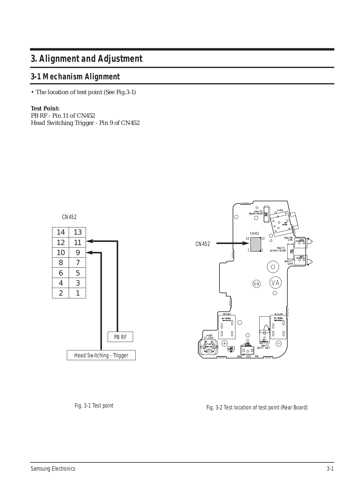
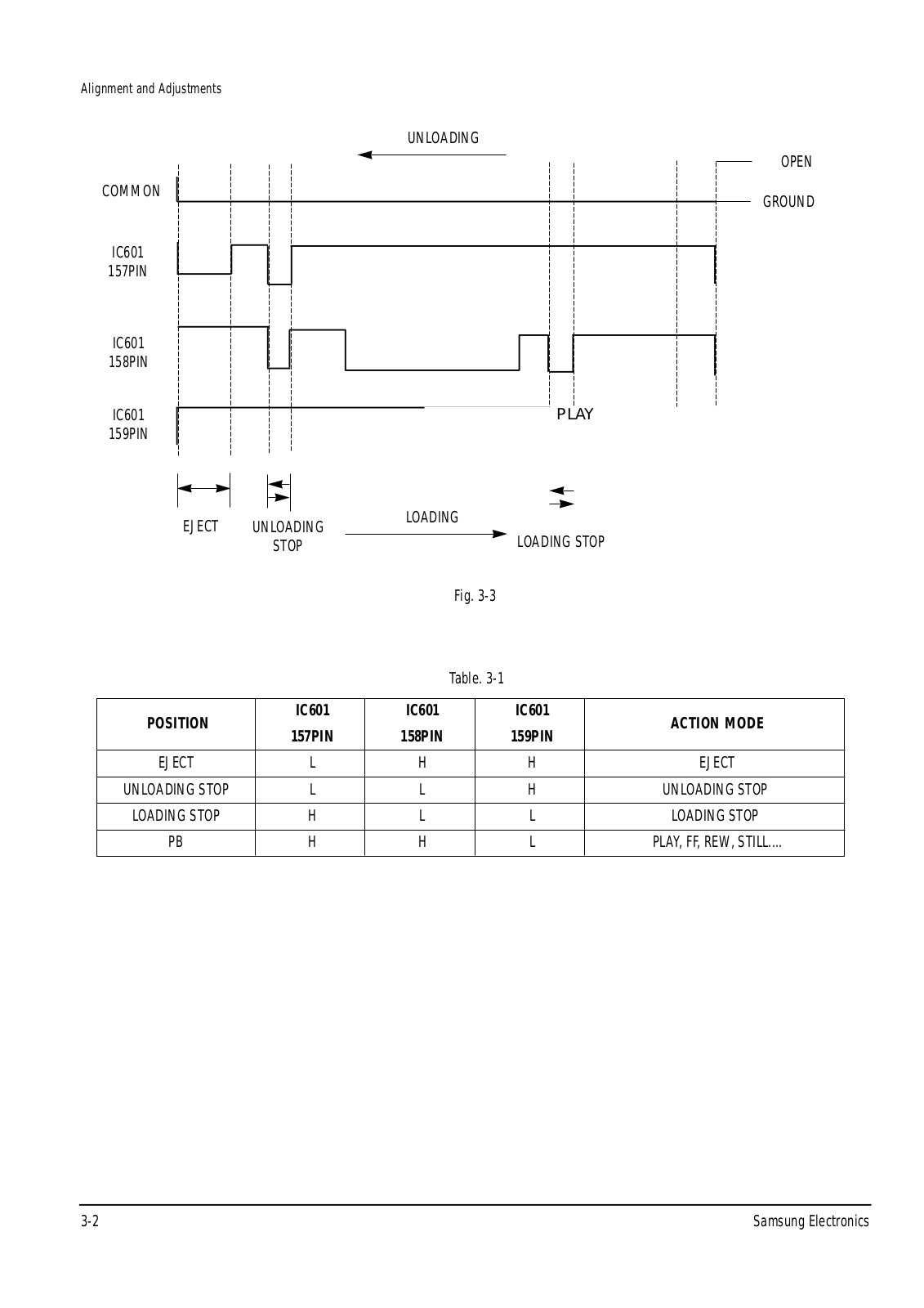
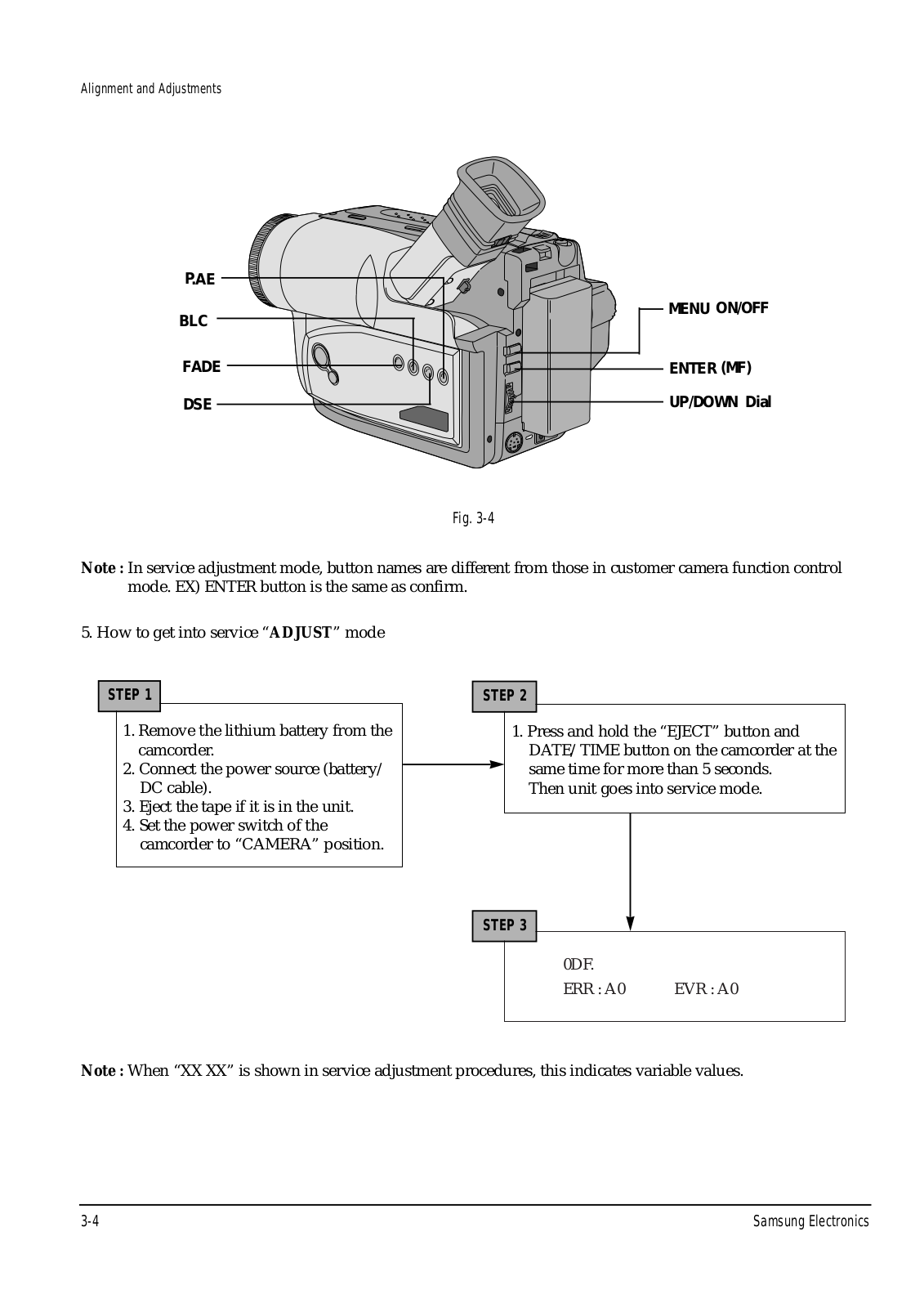
How it Works
Log In / Sign Up
0
My Files
0
My Downloads
203445
History
Account Settings
Log Out
Buy Points
How it Works
FAQ
Contact Us
Questions and Suggestions
Users
show menu
Samsung
Loading...
V
VP-D10
VP-D101
VP-D101(I)
VP-D103
VP-D105I
2
VP-D130
VP-D20
2
VP-D200i
VP-D23
VP-D30
VP-D301
VP-D323
VP-D351
VP-D351i
VP-D361i
VP-D371(i)
VP-D391
VP-D39I
VP-D451
VP-D451(I)
VP-D463
VP-D530
VP-D55
VP-D590I
VP-D6050SI
VP-D655I
VP-D80
VP-D87I
VP-D905
VP-D93
VP-D99I
VP-DC161i
VP-DX100
VP-L10
VP-L500
2
VP-L600
VP-L700
2
VP-L700U
VP-L800
VP-L870
2
VP-L980
VP-M50
2
VP-MM11S
VP-MX10
VP-MX25
VP-W60
VP-W63
VP-W70
3
VP-W80
VP-W80U
VP-W90
2
VP-X105L
VP-X110L
VPD307i
VPD73
2
VP_L100
VR 8559
VR05R5050WK
VR20H9050UW-EU
VR20H9050UW-GE
VR2AJ9040WG/AA
VR2AM7065WS
VR8160
VS15T7031R1/EV
VS20T7532T1
VS60M6015KG/EV
VY-H200
VY-H350
2
W
W200RP
W20NB
W81K6404QW
WA10B7Q1
WA11M8700GV
WA12F5L4
WA13G7Q1
WA17A3
WA1DX
WA400PJHDWR/AA-01
WA40J3000AW/AA-13
WA456DRHDSU
WA456DRHDWR
WA45K7600AW/A2
WA45M7050AW
WA45N3050AW/A4-00
WA45T3200AW
2
WA45T3400AP
WA484DSHAWR/A1
WA48H7400AW-A2
2
WA48H7400AW/AA-11
WA48J7770AW/A2
WA50F9A8DSP
WA50F9A8DSP-A2
WA50F9A8DSW/A2
WA50F9A8DSW/A2-01
WA50K8600AW/A2
WA50M7450AW/A4-00
WA50N7350A
WA50R5200AW
WA50R5400AW
WA50T5300AC
Loading...
Loading...
Nothing found
VP-W90
User Manual [fr]
69 pgs
3.88 Mb
0
User Manual [ru]
64 pgs
3.46 Mb
1
User Manual
68 pgs
3.81 Mb
0
User Manual
65 pgs
3.82 Mb
0
Manual [hu]
66 pgs
3.86 Mb
0
Manual [pt]
66 pgs
3.86 Mb
0
Manual [es]
65 pgs
3.82 Mb
0
Manual [fi]
66 pgs
3.87 Mb
0
Owner's Instruction Manual
65 pgs
3.96 Mb
0
Service manual
89 pgs
8.07 Mb
3
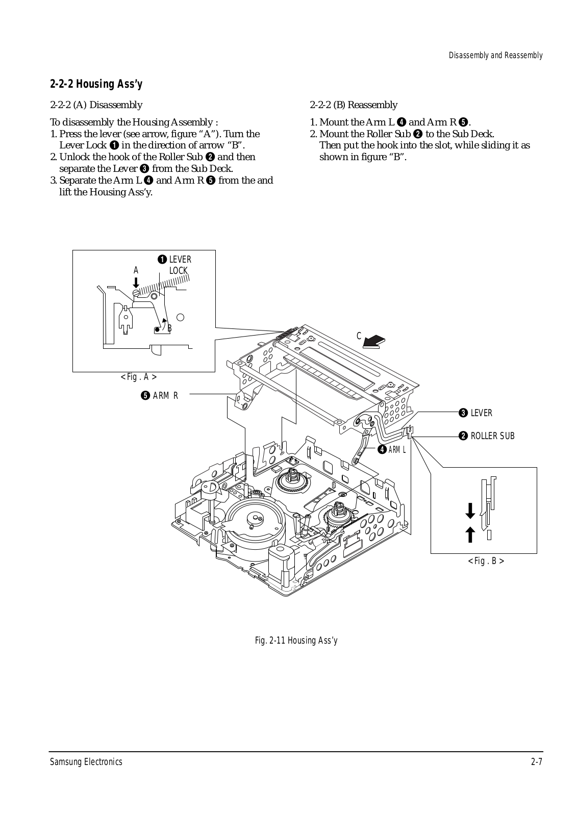
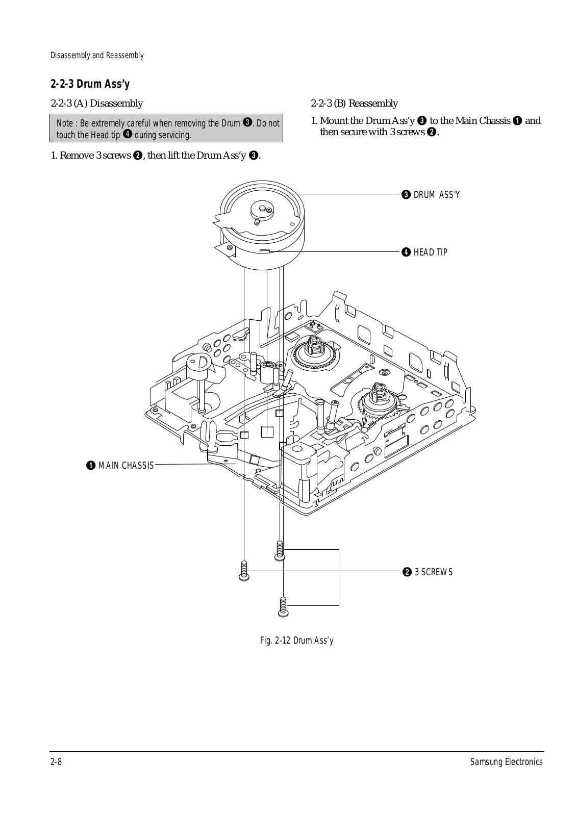
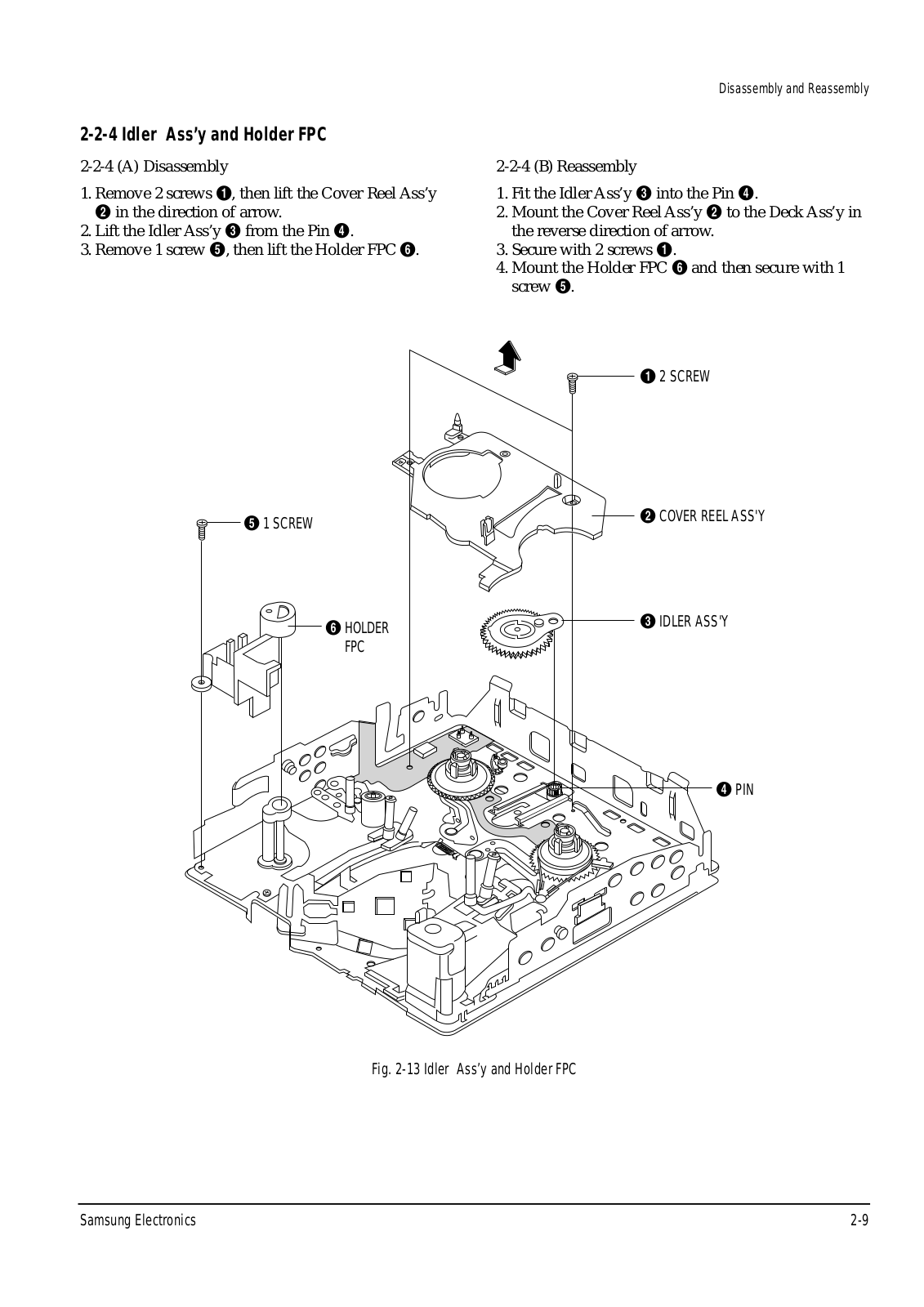
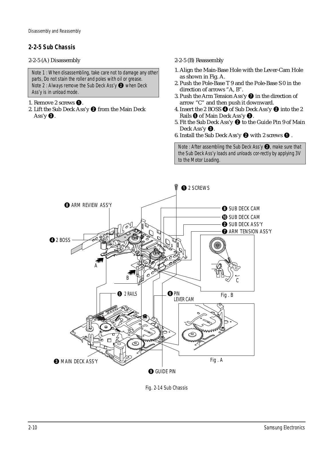
Table of contents
Loading...
Samsung VP-W90, VP-W95D, VP-97 Service manual
...
Samsung Service manual
Download
4.3
(
4
)
Loading...
+
62
hidden pages
Unhide
You need points to download manuals.
1 point = 1 manual.
You can buy points or you can get point for every manual you upload.
Buy points
Upload your manuals


 Loading... Loading...