


 Loading...
ORDER NO. KMS1308957CE
F19
DECT 6.0 Portable Station
Model No. KX-TCA385
(for U.S.A., Canada)
© Panasonic System Networks Co., Ltd. 2013 Unauthorized copying and distribution is a violation of law.

KX-TCA385
TABLE OF CONTENTS
|
PAGE |
PAGE |
|
1 Safety Precautions ----------------------------------------------- |
3 |
9.6.2. No Link problem (BT) ------------------------------ |
40 |
1.1. For Service Technicians --------------------------------- |
3 |
9.7. STM (Start Monitor) ------------------------------------- |
40 |
2 Warning -------------------------------------------------------------- |
4 |
9.8. Error Message-------------------------------------------- |
41 |
2.1. About Lead Free Solder (PbF: Pb free) -------------- |
4 |
9.8.1. Need Repair ----------------------------------------- |
41 |
2.1.1. Suggested PbF Solder ------------------------------- |
4 |
9.8.2. “ERROR 1”, “ERROR 2” -------------------------- |
41 |
2.2. Discarding of P. C. Board -------------------------------- |
4 |
10 Disassembly and Assembly Instructions -------------- |
42 |
3 Specifications ------------------------------------------------------ |
5 |
10.1. Handset ---------------------------------------------------- |
42 |
4 Technical Descriptions------------------------------------------ |
6 |
10.2. PART SETTING (BATTERY COVER and O- |
|
4.1. Block Diagram ---------------------------------------------- |
6 |
RING) ------------------------------------------------------- |
43 |
4.2. Circuit Operations------------------------------------------ |
7 |
10.3. Charger Unit ---------------------------------------------- |
44 |
4.2.1. Outline---------------------------------------------------- |
7 |
11 Measurements and Adjustments-------------------------- |
45 |
4.2.2. Power Supply Circuit / Reset Circuit-------------- |
7 |
11.1. Check Procedure (Handset) -------------------------- |
45 |
4.2.3. Reset Circuit -------------------------------------------- |
7 |
11.1.1. Preparation ------------------------------------------- |
45 |
4.2.4. Clock Circuit -------------------------------------------- |
8 |
11.1.2. PC Setting -------------------------------------------- |
45 |
4.2.5. Bus Access --------------------------------------------- |
8 |
11.2. Adjustment (Handset) ---------------------------------- |
47 |
4.2.6. Charge circuit ------------------------------------------ |
8 |
11.2.1. Equipment Required ------------------------------- |
47 |
4.2.7. Battery Low/Power Down Detector --------------- |
9 |
11.2.2. The Setting Method of JIG------------------------ |
47 |
4.2.8. LCD Circuit-------------------------------------------- |
10 |
11.2.3. Connections (Handset) ---------------------------- |
47 |
4.2.9. LED Circuit -------------------------------------------- |
11 |
12 Miscellaneous --------------------------------------------------- |
50 |
4.2.10. Vib Circuit---------------------------------------------- |
11 |
12.1. Terminal Guide of the ICs Transistors and |
|
4.2.11. RF Circuit---------------------------------------------- |
12 |
Diodes ------------------------------------------------------ |
50 |
4.2.12. Bluetooth Circuit ------------------------------------- |
13 |
12.1.1. Handset ----------------------------------------------- |
50 |
4.2.13. TX Audio Path---------------------------------------- |
14 |
12.1.2. Charger------------------------------------------------ |
50 |
4.2.14. RX Audio Path --------------------------------------- |
15 |
12.2. How To Replace a Flat Package IC----------------- |
51 |
5 Location of Controls and Components------------------ |
16 |
12.2.1. Preparation ------------------------------------------- |
51 |
5.1. Name of Controls----------------------------------------- |
16 |
12.2.2. Removal Procedure -------------------------------- |
51 |
6 Installation Instructions--------------------------------------- |
18 |
12.2.3. Procedure--------------------------------------------- |
51 |
6.1. Charger Connection ------------------------------------- |
18 |
12.2.4. Removing Solder From Between Pins--------- |
51 |
6.2. Battery ------------------------------------------------------ |
18 |
12.3. How to Replace the LLP (Leadless Leadframe |
|
6.2.1. Battery Installation ---------------------------------- |
18 |
Package) IC----------------------------------------------- |
52 |
6.2.2. Charging the Battery-------------------------------- |
18 |
12.3.1. Preparation ------------------------------------------- |
52 |
6.2.3. Battery Information---------------------------------- |
19 |
12.3.2. Caution ------------------------------------------------ |
52 |
6.2.4. Low Battery Warning ------------------------------- |
19 |
12.3.3. How to Remove the IC ---------------------------- |
52 |
6.2.5. Replacing the Battery ------------------------------ |
19 |
12.3.4. How to Install the IC-------------------------------- |
52 |
7 Operating Instructions ---------------------------------------- |
20 |
12.3.5. How to Remove a Solder Bridge---------------- |
53 |
7.1. Soft Keys --------------------------------------------------- |
20 |
13 Schematic Diagram -------------------------------------------- |
54 |
7.2. Handset Setting Menu Layout ------------------------ |
22 |
13.1. Handset ---------------------------------------------------- |
54 |
7.3. Key Lock---------------------------------------------------- |
23 |
13.2. Charger----------------------------------------------------- |
58 |
7.4. Selecting the Display Language---------------------- |
23 |
14 Printed Circuit Board------------------------------------------ |
59 |
7.5. Display ------------------------------------------------------ |
24 |
14.1. Handset ---------------------------------------------------- |
59 |
7.6. Function Menus------------------------------------------- |
25 |
14.1.1. Component View------------------------------------ |
59 |
7.7. Function Keys--------------------------------------------- |
26 |
14.1.2. Bottom View------------------------------------------ |
60 |
7.8. Flexible CO Keys----------------------------------------- |
27 |
14.2. Charger----------------------------------------------------- |
61 |
7.9. Caller ID ---------------------------------------------------- |
28 |
15 Appendix Information of Schematic Diagram -------- |
62 |
7.10. Character Mode Table ---------------------------------- |
29 |
16 Exploded View and Replacement Parts List----------- |
63 |
8 Firmware Version up------------------------------------------- |
30 |
16.1. IC Data ----------------------------------------------------- |
63 |
9 Troubleshooting Guide---------------------------------------- |
33 |
16.1.1. IC1 (APU) --------------------------------------------- |
63 |
9.1. Power ON NG--------------------------------------------- |
33 |
16.1.2. IC100 (DPU) ----------------------------------------- |
65 |
9.2. No Display ------------------------------------------------- |
34 |
16.2. Cabinet and Electric Parts----------------------------- |
68 |
9.3. LED Trouble ----------------------------------------------- |
35 |
16.2.1. Handset ----------------------------------------------- |
68 |
9.3.1. Key backlight does not light----------------------- |
35 |
16.2.2. Charger Unit------------------------------------------ |
69 |
9.3.2. Charge LED (BELL LED) does not light ------- |
35 |
16.3. Accessories and Packing Materials----------------- |
70 |
9.4. Charge problem ------------------------------------------ |
37 |
16.4. Replacement Parts List -------------------------------- |
71 |
9.4.1. Handset ------------------------------------------------ |
37 |
16.4.1. Handset ----------------------------------------------- |
71 |
9.4.2. Charger ------------------------------------------------ |
38 |
16.4.2. Charger Unit------------------------------------------ |
73 |
9.5. Vibrator Trouble------------------------------------------- |
38 |
16.4.3. Accessories and Packing Materials ------------ |
73 |
9.6. RF Trouble ------------------------------------------------- |
39 |
16.4.4. Fixtures and Tools ---------------------------------- |
73 |
9.6.1. No Link problem (DECT) -------------------------- |
39 |
|
|
2

KX-TCA385
1Safety Precautions
1.Before servicing, unplug the AC power cord to prevent an electric shock.
2.When replacing parts, use only the manufacturer's recommended components.
3.Check the condition of the power cord. Replace if wear or damage is evident.
4.After servicing, be sure to restore the lead dress, insulation barriers, insulation papers, shields, etc.
5.Before returning the serviced equipment to the customer, be sure to perform the following insulation resistance test to prevent the customer from being exposed to shock hazards.
1.1.For Service Technicians
•Repair service shall be provided in accordance with repair technology information such as service manual so as to prevent fires, injury or electric shock, which can be caused by improper repair work.
1.When repair services are provided, neither the products nor their parts or members shall be remodeled.
2.If a lead wire assembly is supplied as a repair part, the lead wire assembly shall be replaced.
3.FASTON terminals shall be plugged straight in and unplugged straight out.
•ICs and LSIs are vulnerable to static electricity.
When repairing, the following precautions will help prevent recurring malfunctions.
1.Cover plastic parts boxes with aluminum foil.
2.Ground the soldering irons.
3.Use a conductive mat on worktable.
4.Do not grasp IC or LSI pins with bare fingers.
3

KX-TCA385
2 Warning
2.1.About Lead Free Solder (PbF: Pb free)
Note:
In the information below, Pb, the symbol for lead in the periodic table of elements, will refer to standard solder or solder that contains lead.
We will use PbF solder when discussing the lead free solder used in our manufacturing process which is made from Tin (Sn), Silver (Ag), and Copper (Cu).
This model, and others like it, manufactured using lead free solder will have PbF stamped on the PCB. For service and repair work we suggest using the same type of solder.
Caution
•PbF solder has a melting point that is 50 °F ~ 70 °F (30 °C ~ 40 °C) higher than Pb solder. Please use a soldering iron with temperature control and adjust it to 700 °F ± 20 °F (370 °C ± 10 °C).
•Exercise care while using higher temperature soldering irons.:
Do not heat the PCB for too long time in order to prevent solder splash or damage to the PCB.
•PbF solder will tend to splash if it is heated much higher than its melting point, approximately 1100 °F (600 °C).
•When applying PbF solder to double layered boards, please check the component side for excess which may flow onto the opposite side (See the figure below).
2.1.1.Suggested PbF Solder
There are several types of PbF solder available commercially. While this product is manufactured using Tin, Silver, and Copper, (Sn+Ag+Cu), you can also use Tin and Copper, (Sn+Cu), or Tin, Zinc, and Bismuth, (Sn+Zn+Bi). Please check the manufac turer's specific instructions for the melting points of their products and any precautions for using their product with other materials.
The following lead free (PbF) solder wire sizes are recommended for service of this product: 0.3mm, 0.6mm and 1.0mm.
2.2.Discarding of P. C. Board
When discarding P. C. Board, delete all personal information such as telephone directory and caller list or scrap P. C. Board.
4
KX-TCA385
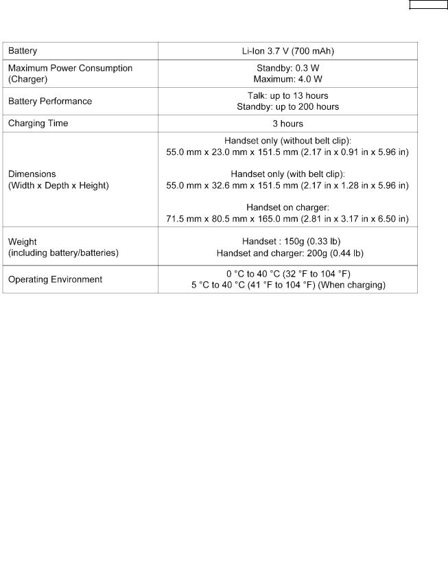
3 Specifications
RF Specifications (DECT 6.0)
RF Specifications (Bluetooth)
5

KX-TCA385
4 Technical Descriptions
4.1.Block Diagram
BL1 LCD |
BL2 LCD |
LCD_Backlight |
|
|
0.5 |
0V.DOUT3 |
|
|
CHG |
CHG0v.5 |
|||
|
|
|
Reg |
|
BT for Supply Power |
0.BT3 |
Supply Power |
LED BELL (RED/GREEN) |
BL2 LCD |
BL1 LCD |
- |
+ |
|
|
|
M |
|
Backlight for |
,& |
|
IC Port I/O |
CHG-IC_ |
Circuit Charger |
||||
|
|
|
0V . 5 |
|
|
|
|
CP_ON |
|
|
|
ON/OFF |
|
|
|
Key_Backlight |
|
|
|
|
|
WakeUPOUTBT |
|
|
|
||
|
|
Vib_Motor |
CTRLVib |
|
ONBT |
|
|
I2C |
StateCHG |
RESETBT |
|
STATUS |
|
|
|
|
|
|
|
|
|
|
|
|
|
|
|
|
|
|
|
|
|
|
|
|
|
DOUT3.0V |
|
||
|
|
|
|
|
|
|
|
|
|
VDDC 1.8 |
|
||
|
|
|
|
|
|
|
|
|
|
|
|
|
|
|
|
|
(DPU) |
BBIC |
|
,& |
|
|
|
|
I/F DPU-APU |
|
RF |
I/F JTAG |
I/F Uart |
I/F PCM |
bus Data / Address |
SPI |
8KBIO1 |
GPIO |
SPOUTP SPOUTN |
|
Li-ion |
|
.3 |
|
|
700mAh / 7v |
|
BAT |
TH |
BAT |
|
- |
|
+ |
|
BATT
DET CHG |
CUR CHG |
VBAT for Supply Power |
0V).VBAT(3 |
BBIC (APU) |
,& |
824MH.13 |
’TALX |
|
|
HSSPOUTP LOUT |
MIN |
MIP |
I/F RF |
|
|
|
|
|
|
|
|
|
Circuit |
RF |
|
|
|
|
|
Diagram Block UDT131-KX
JTAG |
|
(3pin) CON UART |
|
UNIT BT |
|
Cypress (4MBit) SRAM |
|
Winbond (32MBit) Flash Serial |
|
Matrix Triangle26 Key |
|
ICHX8353)-/Dr Truly 128x160dot LCD Color TFT 8”.1 |
|
|
|
- |
|
|
|
|
|
|
|
|
|
|
|
|
|
|
|
SPEAKER |
|
RECEIVER |
MIC |
|
|
|
|
|
|
ANT |
,& |
|
|
|
|
|
|
||||
|
|
|
|
|
|
,& |
|
|
|
|
|
|
|
|
|
|
|
ANT
6

KX-TCA385
4.2.Circuit Operations
4.2.1.Outline
Handset consists of the following ICs as shown in Block Diagram (Handset).
•BBIC (Base Band IC): IC100
-All data signals (forming/analyzing ACK or CMD signal)
-All interfaces (ex: Key, Detector Circuit, Charge, LCD, LED, SRAM, Flash ROM)
•SRAM: IC101
-Application data and code are temporarily stored.
•Flash ROM (substitute EEPROM): IC102
-Adjustment data, program data and temporary user data are stored.
•RF IC: IC1
-PLL Oscillator
-Detector
-Compress/Expander
-Amplifier for reception
-Amplifier for transmission
•Bluetooth Unit: IC601
4.2.2.Power Supply Circuit / Reset Circuit
The power supply of each IC is as follows.
The Power On Reset is designed to guarantee power-on of the system only when 1.8v and 3.0v voltages exist.
4.2.3.Reset Circuit
The reset signal is generated with IC1(44Pin).
When VBAT3V that is IC202's output exceeds 1.7V, release the Reset
7

KX-TCA385
4.2.4.Clock Circuit
4.2.5.Bus Access
The SRAM is used with an async mode.
4.2.6.Charge circuit
Circuit Operation:
When charging with Charger, the charge current is as follows:
DC+(5.5V) → F1(Charger) → D1(Charger) → IC1(Charger) → L1(Charger) → CHARGE+(Charger) → CHARGE+(Handset) → IC203 → F201 → BATTERY+... BATTERY- → R201 → GND → CHARGE-(Handset) → CHARGE-(Charger) → L2(Charger) → GND(Charger)
In this way, the BBIC(IC1) on Handset detects the fact that the battery is charged.
The charge current is controlled by IC203 of Handset.
Include Charger
Charger current
J1 |
|
5 |
CONT |
|
CS 4 |
|
|
F1 D1 |
6 |
NC2 |
FIN |
GND 3 |
C3 |
||
1 |
7 |
NC3 |
NC1 2 |
||||
|
|||||||
|
|
8 |
VIN |
|
VO 1 |
GND |
29
|
IC1 |
GND |
|
GND |
C1 |
L1 |
TP3 |
|
|
|
CHG+ |
|
GND GND |
|
|
|
|
C2 |
|
|
|
L2 |
TP4 |
|
|
|
CHG- |
|
|
GND |
|
Charger
|
CHG+ |
|
1 |
CN201 |
C211 |
|
|
|
|
|
GND |
|
|
R209 |
|
|
R208 |
1 |
CN202 |
GND |
|
CHG- |
GND |
Handset
|
|
|
|
|
|
F201 |
|
|
|
|
|
|
IC203 |
|
C206 |
|
|
|
|
||
|
|
|
|
|
|
|
+ |
|
||
|
|
|
11 |
C218 |
|
GND |
|
|
|
|
|
|
|
|
|
|
|
|
|
||
|
R220 |
1 VCC |
BAT 10 |
|
|
|
|
Li-ION |
|
|
|
2 ROSC |
VSENSE 9 |
|
|
|
|
TH |
Battery |
|
|
C213 |
|
R216 |
|
COUNT |
|
- |
|
|||
|
3 LED |
FIN RICHG 8 |
|
|
|
|
||||
|
|
4 GND |
TMRCNT 7 |
GND |
|
CHG_CUR |
|
|||
|
|
5 VDD |
TH 6 |
|
|
|||||
|
|
R219 |
R217 |
|
C206 |
|||||
|
GND |
|
R218 |
|
L2 |
|
R201 |
|||
|
|
|
|
|
|
|
|
|
|
|
|
|
|
|
|
GND |
|
|
|
|
|
|
|
|
|
GND |
|
10 |
|
7 |
|
|
|
|
R210 |
|
CHG_DET |
24 |
|
|
GND |
|
|
|
|
R211 |
|
|
|
IC1 |
|
|
|
|
|
|
GND |
|
|
|
|
|
|
|
|
|
|
|
CHG_state |
8824 |
|
|
|
|
||
|
|
|
|
|
|
|
|
|
|
|
IC100
8

KX-TCA385
•The charge current is controlled by IC203 of Handset. Charge current characteristic is as follows.
Charging method is CCCV. (CC: constant current, CV: constant voltage)
|
|
V, I |
|
|
|
CC charge |
CV charge |
voltage |
4.2 |
V |
|
Battery |
3.97 |
V |
|
|
|
||
|
0 V |
|
|
Charge stop |
CC charge |
CV charge |
Charge stop |
Recharge
Charge current
I mA 


Charge complete
I/10 mA
0 mA  t
t
• IC100-88pin (CHG_state)
IC100-88pin (CHG_state) |
Charge controll |
|
|
High |
Charging |
|
|
Low |
Charge complete |
|
|
• When handset is put on charger, handset detects battery charge.
Charge detect |
IC1-24pin (CHG_DET) |
Charge LED (Red LED) |
|
|
|
ON |
Above 1.5V |
ON |
|
|
|
OFF |
Below 1.2V |
OFF |
|
|
|
• TH(IC203-6pin) is temperature detecting pin of battery.
The charge temperature range is 5 degree C to 40 degree C.
If charge temperature is above 40 degree C or below 5 degree C, charge stops.
Charge |
Battery temperature |
|
|
|
|
ON |
0 |
°C to 40 °C |
|
|
|
OFF |
Below 5 |
°C or above 40 °C |
|
|
|
4.2.7. Battery Low/Power Down Detector
"Battery Low" and "Power Down" are detected by BBIC (IC1) which checks the battery voltage. The detected voltage is as follows;
• Battery Low
Battery voltage: V(Batt) 3.4V ± 50mV |
|
The BBIC detects this level and " |
“ starts flashing. |
• Power Down
Battery voltage: V(Batt) 3.2V ± 50mV
The BBIC detects this level and power down.
9

KX-TCA385
4.2.8.LCD Circuit
•The LCD is controlled by SPI (LCD_SCL, LCD_RESET, LCD_CS, LCD_SID, LCD_CD).
•LCD back-light has 3 modes ( Brightness 1/2/3*) and back-light OFF. *Brightness level: Brightness 1 > Brightness 2 > Brightness 3
Back-light Mode |
IC401-4pin (CP_ON) |
IC401-2pin (LCD_BL1) |
IC401-3pin (LCD_BL2) |
|
|
|
|
Brightness 1 |
High |
High |
High |
|
|
|
|
Brightness 2 |
High |
High |
Low |
|
|
|
|
Brightness 3 |
High |
Low |
Low |
|
|
|
|
Back-light OFF |
Low |
Low |
Low |
|
|
|
|
10
KX-TCA385
4.2.9.LED Circuit
• DPU(IC100) controls each LEDs.
Type of LED |
LED ON |
LED OFF |
Bell LED (Green) |
IC401-7pin = High |
IC401-7pin = Low |
LED531 |
|
|
Bell LED (RED) |
IC401-5pin = High |
IC401-5pin = Low |
LED530 |
|
|
Key back-light LEDs (White) |
IC401-3pin = High |
IC401-3pin = Low |
LED520 - LED525 |
(Q521 = ON) |
(Q521 = OFF) |
|
|
|
4.2.10. Vib Circuit
• Vibrator is controlled by IC1-23 pin.
|
VIB ON |
VIB OFF |
IC1-23 pin |
High |
Low |
VOUT of IC501 |
1.4V |
0V |
11

KX-TCA385
4.2.11.RF Circuit
Reception
A digital voice signal from LAN is received as "TX_DATA" (*1) by DMW in a cell station.
Then TX_DATA goes to RF part, and it's modulated to 1.9 GHz RF signal. The RF signal is amplified and fed to a selected antenna by antenna diversity .
As for a portable station, RF signal of cell station is received in two antennas.
RFIC(IC1) of portable station compares RF signal levels from cell station and selects the antenna to be used.
RX signal in the selected antenna is amplified and down-converted to 864 kHz IF signal, then demodulated to digital data "RX_DATA".
RFIC(IC1) converts RX_DATA into a voice signal and outputs it to speaker.
Transmission
A voice signal from microphone is encoded to digital data "TX_DATA" by RFIC(IC1) in a portable station.
TX_DATA goes to RF part, and it's modulated to 1.9 GHz RF signal. The RF signal is amplified and fed to a selected antenna by antenna diversity.
As for a cell station, RF signal is received in two antennas.
RFIC of cell station compares RF signal levels from portable station and selects the antenna to be used.
RX signal in the selected antenna is amplified and down-converted to 864 kHz IF signal, then demodulated to digital data "RX_DATA".
DMW is received RX_DATA (*1) as a voice signal from portable station and outputs it to LAN.
Note:
(*1) TX_DATA and RX_DATA are bundled to one signal as "RXTXDATA" of DMW in cell station.
Antenna diversity |
TX_RF |
|
|
CL2 |
|
|
|
|
|
|
|
|
|
|
|
|
|
|
|
|
|
|
|
|
|
L32 |
|
|
|
|
|
|
|
|
|
AT_JP2 |
|
|
|
|
|
|
|
|
|
|
|
|
|
|
|
|
|
|
|
|
|
|
|||
|
|
|
|
|
|
|
|
|
|
|
|
|
|
|
|
|
|
|
|
|
|
|
|
|
|
|
|
||
|
|
|
|
12 |
ANT_TP2 |
|
|
|
|
|
|
|
|
|
|
|
|
|
|
|
|
C37 |
2.2n |
|
TX_RF |
||||
|
|
C49 |
|
|
12 |
|
|
|
|
|
|
|
|
|
|
|
|
|
|
|
|
NC |
|
|
|||||
|
|
|
|
|
|
|
|
|
|
|
|
|
|
|
|
|
|
|
|
|
|
|
|
|
|
|
|
||
|
|
|
1n |
10n |
|
|
|
|
|
|
|
|
|
|
|
|
|
|
C36 |
|
|
|
GND |
|
|
|
|
|
|
|
|
|
L39 |
|
GND |
|
|
|
|
|
|
|
|
|
|
|
|
10p |
|
|
|
|
|
|
|
|
|
|
|
|
|
|
GND |
|
L38 |
0 |
|
|
|
|
|
L30 4.7n |
|
|
|
|
|
|
C35 |
1.5p |
|
C34 |
1.5p |
|
|
|
|
||
|
|
|
|
D50 |
|
|
C62 |
NC |
|
|
C30 |
|
1p |
C31 |
1.5p |
C48 |
|
|
|
|
GND |
|
|
|
|
|
|
||
|
|
|
|
|
|
|
|
|
10p |
|
|
|
|
|
|
|
|
|
|
||||||||||
|
|
|
|
|
|
|
|
|
|
|
|
|
|
|
|
|
|
|
|
|
|
|
|
|
|
|
|
|
|
|
|
|
|
GND |
|
|
GND |
|
|
|
GND |
GND |
RX_RF |
|
|
|
|
|
|
|
|
|
|
|
|
|
|||
|
|
AT_JP1 |
|
|
|
|
|
|
|
|
|
|
|
|
|
|
|
GND |
|
|
|
|
|
||||||
|
C51 |
L43 |
12 |
ANT_TP1 |
|
|
|
|
|
|
|
|
|
|
|
|
|
|
|
|
|
|
|
|
|
|
|
|
|
|
|
12 |
|
|
|
|
|
|
|
|
|
|
|
|
|
|
|
|
|
|
|
|
|
|
|
|
|
||
|
CL1 |
1n |
|
|
|
|
|
|
|
|
|
|
|
|
|
|
|
|
|
|
|
|
|
|
|
|
|
|
|
|
|
|
|
|
|
|
|
|
|
|
|
|
|
|
|
|
|
|
|
|
|
|
|
|
|
|
|
||
|
0 |
|
|
|
|
|
|
|
|
|
|
|
TX_RF |
|
|
|
|
RX_RF |
|
|
C52 |
|
|
||||||
VCC_PA |
L40 |
1p |
|
GND |
|
|
|
|
|
|
|
|
|
|
|
|
|
GND |
3p |
|
|||||||||
BAL_OUT2 |
|
|
|
|
L42 |
0 |
|
|
|
L31 2.7n |
|
|
|
|
L35 |
|
|
|
|
|
C47 |
L33 33p |
|
|
|||||
BAL_OUT1 |
|
|
|
|
|
|
|
|
|
|
|
|
|
|
|
|
|
|
|||||||||||
TX_SW |
|
GND |
|
|
|
|
|
|
|
|
|
|
|
C50 |
|
|
|
2.7n |
|
|
|
|
|
5.6n |
|
|
|
|
|
ANT1 |
|
|
|
|
|
|
|
|
|
|
|
|
|
|
|
|
C41L34 |
5.1n |
C53 |
|
|
|
|
|
|||||
RX_SW |
|
|
D51 |
|
|
C61 |
NC |
|
C32 |
1p |
C33 |
1.5p |
10p |
|
C43 |
NC |
C42 |
3p |
NC |
C39 |
1.5p |
|
|
|
|||||
LNA_INP |
|
|
|
|
|
|
|
|
5p |
GND |
GND |
|
|
|
|||||||||||||||
TO RF BLOCK |
|
|
|
|
|
|
|
|
|
|
|
|
|
|
|
|
|
|
|
|
|
|
|
|
|
|
|
|
|
ANT2 |
|
|
|
|
|
|
|
|
|
|
|
|
|
|
|
|
|
|
|
|
|
|
|
|
|
|
|
|
|
LNA_INN |
|
|
|
|
|
|
|
|
|
|
|
|
|
|
|
|
|
|
|
|
|
|
|
|
|
|
|
|
|
|
|
|
|
GND |
|
GND |
|
|
GND |
|
|
GND |
|
|
|
|
|
|
|
|
|
|
|
|
|
|
|
|
|
|
|
|
|
|
|
|
|
|
|
|
|
|
|
|
|
|
|
|
|
|
|
|
|
|
|
|
|
||
|
|
|
|
|
|
|
|
|
|
|
|
|
|
|
GND |
|
GND |
GND |
|
|
|
|
|
|
|
||||
|
|
|
|
|
|
|
|
|
|
|
|
|
|
|
|
|
|
|
|
|
|
|
|
||||||
VBAT_3.0V |
|
|
|
|
|
|
|
|
|
|
|
|
|
|
|
|
|
|
|
|
|
|
|
|
|
33n |
|
|
|
|
|
|
|
|
|
|
|
|
|
|
|
|
|
|
|
|
RX_RF |
|
|
|
|
|
|
|
|
|
|||
C1 |
1u |
|
|
|
|
|
|
|
|
|
|
|
|
|
|
|
|
|
|
|
|
|
|
L36 |
|
|
|||
C58 |
|
|
|
|
|
|
|
|
|
|
|
|
|
|
|
|
|
|
|
|
|
|
|
|
C45 |
0.5p |
C44 |
100p |
|
0.2p |
|
|
|
|
|
|
|
|
|
|
|
|
|
|
|
|
|
|
|
|
|
|
|
|
|||||
|
C3 |
|
|
|
|
|
|
|
|
|
|
|
|
|
|
|
|
|
|
|
|
|
|
|
|
GND GND |
|
||
|
|
|
|
|
|
|
|
|
|
|
|
|
|
|
|
|
|
|
|
|
|
|
|
|
|
|
|
|
|
|
|
|
|
|
|
|
|
|
|
|
|
|
|
|
|
|
|
|
|
|
|
|
|
|
|
|
|
|
|
|
|
|
|
|
|
|
|
|
|
|
|
|
|
|
|
|
|
|
|
|
|
|
|
|
|
|
|
|
|
|
|
|
|
|
|
|
1u |
|
|
|
|
|
|
|
|
|
|
|
|
|
|
|
|
|
|
|
|
|
|
||||||
|
|
|
|
|
|
|
|
|
|
|
|
|
|
|
|
|
|
|
|
|
|
|
|
|
|
|
|
|
|
|
|
|
|
GND |
|
|
|
|
|
|
|||||||
51 |
|
50 |
|
49 |
|
48 |
|
47 |
|
46 |
|
45 |
|
44 |
43 |
|
42 |
|
41 |
|
40 |
|
39 |
|
38 |
|
37 |
|
36 |
|
35 |
|
|
|
|
|
|
|
|
|
|
||||||
|
|
|
|
|
|
|
|
|
|
|
|
|
|
|
|
|
|
|
|
|
|
|
|||||||||||||||||||||||||
IF_EN_DA IFRX1 |
IF MLSE |
IFT DATA |
OFFON OUT ON OFF VCCVCO RSTN P/EXTATSTLNA ATST N LNA INP |
LNA INN RX SW TEST ANT2 GND RF |
BAL_OUT2 |
32 |
|
|
|
|
|||||||||||||||||||||||||||||||||||||
_IF NPORST |
|
|
|
|
|
|
|
|
|
|
|
|
|
|
|
|
|
|
|
|
|
|
|
|
|
|
|
|
|
|
|
|
ANT1 |
34 |
|
|
|
|
|||||||||
IF_NARES |
|
|
|
|
|
|
|
|
|
|
|
|
|
|
|
|
|
|
|
|
|
|
|
|
|
|
|
|
|
|
|
|
|
|
TX_SW |
|
|
|
|
||||||||
|
|
|
|
|
|
|
|
|
|
|
|
|
|
|
|
|
|
|
|
|
|
|
|
|
|
|
|
|
|
|
|
|
|
|
|
|
|||||||||||
|
|
|
|
|
|
|
|
|
|
|
|
|
|
|
|
|
|
|
|
|
|
|
|
|
|
|
|
|
|
|
|
33 |
|
|
|
|
|||||||||||
IF_INT_ANA |
|
|
|
|
|
|
|
|
|
|
|
|
|
|
|
|
|
|
|
|
|
|
|
|
|
|
|
|
|
|
|
|
BAL_OUT1 |
|
|
|
|
|
|||||||||
|
|
|
|
|
|
|
|
|
|
|
|
|
|
|
|
|
|
|
|
|
|
|
|
|
|
|
|
|
|
|
|
|
|
|
|
|
|
||||||||||
|
|
|
|
|
|
|
|
|
|
|
|
|
|
|
|
|
|
|
|
|
|
|
|
|
|
|
|
|
|
|
|
|
|
|
|
|
|
|
|
|
|
|
|
|
|
||
IF_EN_AD |
|
|
|
|
|
|
|
|
|
|
|
|
|
|
|
|
|
|
|
|
|
|
|
|
|
|
|
|
|
|
|
|
|
|
VCC_PA |
|
31 |
(1608) |
|||||||||
|
|
|
|
|
|
|
|
|
|
|
|
|
|
|
|
|
|
|
|
|
|
|
|
|
|
|
|
|
|
|
|
|
|
||||||||||||||
|
|
|
|
|
|
|
|
|
|
|
|
|
|
|
|
|
|
|
|
|
|
|
|
|
|
|
|
|
|
|
|
|
30 |
||||||||||||||
IF_DATA_DA |
|
|
|
|
|
|
|
|
|
|
|
|
|
|
|
|
|
|
|
|
|
|
|
|
|
|
|
|
|
|
|
|
VCC_FE_IF |
|
|||||||||||||
|
|
|
|
|
|
|
|
|
|
|
|
|
|
|
|
|
|
|
|
|
|
|
|
|
|
|
|
|
|
|
|
|
|
||||||||||||||
|
|
|
|
|
|
|
|
|
|
|
|
|
|
|
|
|
|
|
|
|
|
|
|
|
|
|
|
|
|
|
|
|
29 |
|
C21 2.2u |
||||||||||||
IF_DATA_AD |
|
|
|
|
|
|
|
|
|
|
|
|
IC1 |
|
|
|
|
|
|
|
|
|
|
|
|
|
VDD_IF |
|
|
|
|
|
|
||||||||||||||
|
|
|
|
|
|
|
|
|
|
|
|
|
|
|
|
|
|
|
|
|
|
|
|
28 |
|
|
|
||||||||||||||||||||
IF_CLK_PLL |
|
|
|
|
|
|
|
|
|
|
|
|
|
|
|
|
|
|
|
|
|
|
|
VBAT_APU |
|
|
|
|
|
|
|||||||||||||||||
|
|
|
|
|
|
|
|
|
|
|
|
|
|
|
|
|
|
|
|
|
|
|
|
27 |
|
C19 (1608) |
|||||||||||||||||||||
IF_CLK_IF |
|
|
|
|
|
|
|
|
|
|
|
|
|
|
|
|
|
|
|
|
|
|
|
|
|
VDD_APU |
|
|
|||||||||||||||||||
|
|
|
|
|
|
|
|
|
|
|
|
|
|
|
|
|
|
|
|
|
|
|
|||||||||||||||||||||||||
|
|
|
|
|
|
|
|
|
|
|
|
|
|
|
|
|
|
26 |
10u |
||||||||||||||||||||||||||||
IF_CDC_DIR |
|
|
|
|
|
|
|
|
|
|
|
|
|
|
|
|
|
|
|
|
|
|
|
|
|
|
|
|
|
|
|
|
|
|
XIN |
|
|||||||||||
|
|
|
|
|
|
|
|
|
|
|
|
|
|
|
|
|
|
|
|
|
|
|
|
|
|
|
|
|
|
|
|
|
|
||||||||||||||
|
|
|
|
|
|
|
|
|
|
|
|
GND |
|
|
|
|
|
|
|
|
|
|
|
|
25 |
||||||||||||||||||||||
IF_CDC_DAT_DA |
|
|
|
|
|
|
|
|
|
|
|
|
|
|
|
|
|
|
|
|
|
|
XOUT |
|
|
|
|
|
|||||||||||||||||||
|
|
|
|
|
|
|
|
|
|
|
|
|
|
|
24 |
|
|
|
|
||||||||||||||||||||||||||||
IF_CDC_DAT_AD |
|
|
|
|
|
|
|
|
|
|
|
|
|
|
|
|
|
|
|
|
|
|
|
|
|
|
|
|
|
|
|
DCINS |
|
|
|
|
|||||||||||
|
|
|
|
|
|
|
|
|
|
|
|
|
|
|
|
|
|
|
|
|
|
|
|
|
|
|
|
|
|
|
|
|
|
|
|||||||||||||
|
|
|
|
|
|
|
|
|
|
|
|
|
|
|
|
|
|
|
|
|
|
|
|
|
|
|
|
|
23 |
|
|
|
|
||||||||||||||
IF_BAT_OK |
|
|
|
|
|
|
|
|
|
|
|
|
|
|
|
|
|
|
|
|
|
|
|
|
|
|
|
|
|
|
|
|
|
|
PWM0 |
|
|
|
|
||||||||
|
|
|
|
|
|
|
|
|
|
|
|
|
|
|
|
|
|
|
|
|
|
|
|
|
|
|
|
|
|
|
|
|
|
|
|
|
|
||||||||||
|
|
|
|
|
|
|
|
|
|
|
|
|
|
|
|
|
|
|
|
|
|
|
|
|
|
|
|
|
|
|
|
22 |
|
|
|
|
|||||||||||
VDD_ADIF |
|
|
|
|
|
|
|
|
|
|
|
|
|
|
|
|
|
|
|
|
|
|
|
|
|
|
|
|
|
|
|
|
|
|
LOUT |
|
|
|
|
||||||||
|
|
|
|
|
|
|
|
|
|
|
|
|
|
|
|
|
|
|
|
|
|
|
|
|
|
|
|
|
|
|
|
|
|
|
|
|
|
||||||||||
ANT2
RX_SW
LNA_INN
LNA_INP
TX_SW
BAL_OUT1
BAL_OUT2
VCC_PA
ANT1
12

KX-TCA385
4.2.12. Bluetooth Circuit
Technical Description for BT unit
1.WHEN IP DATA FOR INCOMING SIGNAL ENTERS FROM IP LINE
a.If KX-TCA385 doesn’t have the registered Bluetooth (BT) Headset, the BT module(IC601) doesn’t work and the BT Headset function can’t use.
b.If KX-TCA385 has the registered Bluetooth Headset,
IC100 (BBIC) inform “incoming call” data to the BT Module by serial Communication (RF/IF) The BT module inform “incoming call” data to the BT Headset by radio transmission.
It is as follows and, specifically, the BT Module generates the radio transmission data and the is radiated.
c.BT Headset detected “incoming call Data”.
BT Headset tells the operator having received a message in “Incoming call”.
2.WHEN A CALLING IS MADE BY THE BLUETOOTH(BT) HEADSET
a.When the operator of BT Headset switches STANDBY to TALK,
TALK mode data enters KX-TCA385 and it is demodulated at the BT module of KX-TCA385.
b.Voice signal is connected between IC100(BBIC) and BT module in a PCM Format. The item of the following explains the operation of transmission and receiver.
3.BT MODULE UNIT RECEIVER OPERATION
BT RF signal is received by a single pattern antenna.
4.BT MODULE UNIT TRANSMISSION OPERATION
BT RF signal is transmitted by a single pattern antenna.
|
|
|
|
|
BT3.0V |
R605 |
|
|
Rx_RF |
|
|
|
|
|
|
BT_ANT |
|
|
L41 |
|
R603 |
|
|
|
L601 |
|
|
|
|
||
|
|
|
|
|
|
|
|
|
|
|
|
|
|
|
Q601 |
GND |
|
Tx_RF |
|
GAP |
R602 |
Tx_Data |
|
GND |
ANT_BT |
|
|||||
|
|
|
|
|
|
|
|
|
GND |
2 |
1 |
|
GND |
|
|
|
|
|
|
|
|||
Bluetooth Unit
BT3.0V |
C601 |
|
23 22 21 20 19 18 17 16 |
|
|
|||
|
GND11 |
GND10 |
GND9 GND8 RF GND7 GND6 |
GND5 |
|
|
24 |
PIO1 |
|
|
|
|
|
25 |
PIO2 |
|
|
GND4 |
15 |
|
26 |
GND12 |
|
|
RESETB |
14 |
|
27 |
VCC |
IC601 |
SPI_CLK |
13 |
||
28 |
GND13 |
SPI_MISO |
12 |
|||
29 |
USB_D+ |
|
|
SPI_CSB |
11 |
|
30 |
USB_D- |
|
OUT |
SPI_MOSI |
10 |
|
32 |
PCM_CLK SYNC |
RTS |
8 |
|
||
31 |
PCM_IN |
|
|
TX |
9 |
|
|
GND1 |
PCM_ |
PCM_ GND2 CTS RX GND3 |
|
|
|
|
1 2 3 4 5 6 7 |
|
|
|
||
GND
BT3.0V |
|
R607 |
R606 |
|
Q602 |
Rx_Data
SPI_CLK
SPI_MISO
SPI_CSB
SPI_MOSI
13
KX-TCA385
4.2.13. TX Audio Path
Microphone
An audio signal from microphone is input to pin 14 (MIC+) and pin 13(MIC-) of IC.
In IC1, the audio signal is converted from the analog signal to ADPCM, then to burst data, and sent to RF cricuit. The stabilized supply voltage is fed to the microphone from pin 17 (MPWR) of IC1.
To reduce consumption current, this voltage is supplied only while calling or receiving.
|
|
|
|
|
51 50 49 48 47 46 45 44 43 42 41 40 39 38 37 36 35 |
|
|
|
|
|
VBAT_3.0V |
|
|
|
|
|
|
|
|
|
|
|
|
|
|
|
|
|
|
|
|||||||||||||
|
C4 |
|
|
|
|
IF RX1 IF MLSE IFT DATA |
OFFON OUT ON OFF VCCVCO RSTN |
P/EXTATSTLNA ATST N LNA INP |
LNA INN |
RX SW |
TEST ANT2 |
GND RF |
BAL_OUT2 32 |
|
|
L21 |
C54 |
|
|
|
|
|
|
|
|
|
|
|
|
|
|
|
|
|
|
|
|
||||||
|
|
|
54 |
IF_EN_DA |
|
|
|
|
|
|
|
|
|
|
|
|
|
|
|
|
|
|
|
|
|
|
|
|
|||||||||||||||
|
|
|
|
52 |
_IF NPORST |
|
|
|
|
|
|
|
|
|
|
|
ANT1 |
34 |
|
|
|
|
|
|
|
|
|
|
|
|
|
|
|
|
|
|
|
|
|
|
|
|
|
|
|
|
|
IF_NARES |
|
|
|
|
|
|
|
|
|
|
|
|
TX_SW |
|
|
|
|
|
|
|
|
|
|
|
|
|
|
|
|
|
|
|
|
|
|
|
|
||
|
|
|
|
53 |
IF_INT_ANA |
|
|
|
|
|
|
|
|
|
|
BAL_OUT1 |
33 |
|
|
|
C59 |
|
|
|
|
|
|
|
|
|
|
|
|
|
|
|
|
|
|
|
|
||
|
|
|
|
55 |
IF_EN_AD |
|
|
|
|
|
|
|
|
|
|
|
|
VCC_PA |
31 |
(1608) |
|
C18 |
|
|
|
|
|
|
|
|
|
|
|
|
|
|
|
|
|
|
|
|
|
0 |
|
|
|
56 |
IF_DATA_DA |
|
|
|
|
|
|
|
|
|
|
VCC_FE_IF |
30 |
|
|
|
|
|
|
|
|
|
|
|
|
|
|
|
|
|
|
|
|
|
|
||||
|
|
|
57 |
IF_DATA_AD |
IC1 |
|
|
|
|
|
|
|
|
VDD_IF |
29 |
C21 |
|
C60 |
|
C17 |
|
|
2 |
1 |
|
|
|
|
|
|
|
|
|
|
|
|
|
|
|
||||
2 |
|
|
|
59 |
IF_CLK_IF |
|
|
|
|
|
|
|
|
|
VDD_APU |
27 |
C19 (1608) |
|
|
|
|
|
|
|
|
|
|
|
|
|
|
|
|
|
|
||||||||
|
|
|
|
58 |
IF_CLK_PLL |
|
|
|
|
|
|
|
|
|
|
VBAT_APU |
28 |
|
|
|
|
|
R14 |
|
|
X1 |
|
|
|
|
|
|
|
|
|
|
|
|
|
|
|||
4 |
|
|
|
61 |
IF_CDC_DIR |
|
|
|
|
|
|
|
|
|
|
|
XIN |
25 |
|
|
|
|
GND |
4 |
3 |
|
|
|
|
|
|
|
|
|
|
|
|
|
|
||||
3 |
|
|
|
60 |
|
|
GND |
|
|
|
|
|
|
|
|
|
|
26 |
|
|
|
|
|
|
|
|
|
|
|
|
|
|
|
|
|
|
|
|
|
|
|
|
|
5 |
|
|
|
62 |
IF_CDC_DAT_DA |
|
|
|
|
|
|
|
|
|
XOUT |
24 |
|
|
CHG_DET |
VBAT_3.0V |
C16 |
|
|
|
|
|
|
|
|
|
|
|
|
|
|
|
|
|
|
|
|||
|
|
|
IF_CDC_DAT_AD |
|
|
|
|
|
|
|
|
|
|
|
DCINS |
|
|
|
|
|
|
|
|
|
|
|
|
|
|
|
|
|
|
|
|
|
|||||||
C23 |
|
|
63 |
IF_BAT_OK |
|
|
|
|
|
|
|
|
|
|
|
PWM0 |
23 |
|
|
VIB_CTRL |
|
GND |
|
|
|
|
|
|
|
|
|
|
|
|
|
|
ZA4 |
|
|||||
|
|
64 |
VDD_ADIF |
|
|
|
|
|
|
|
|
|
HSMIP |
|
LOUT |
22 |
C40 |
|
C15 |
|
|
C324 |
|
|
|
|
|
|
|
|
C329 |
C330 |
D304 |
D305 |
|
1 |
4 |
Speaker |
|||||
(1608) |
C6 |
|
|
65 |
DOUBCAPP2 DOUBCAPN1 DOUBCAPP1 DOUT3V0 DOUT4V5 DOUT2V5/DCIN0/LIN0 LEDSINK2/DCIN1 DCIN2 DCIN3/LIN1 LEDSINK1/PWM1 VREF VCCA MIN MIP HSMIN |
MPWR |
21 |
|
|
|
C323 |
|
|
|
|
|
|
|
|
|
|
4 |
1 |
||||||||||||||||||||
|
L1 |
22u |
66 |
COREOUT |
|
|
|
|
|
|
|
|
|
|
|
|
SPOUTN |
20 |
|
|
|
|
|
|
|
|
|
Speakerphone_SP- |
|
|
|
|
|
|
|
|
|
5 |
|
|
|||
|
|
67 |
VBAT |
|
|
|
|
|
|
|
|
|
|
|
|
VCCPA |
19 |
|
|
|
|
|
|
|
|
|
Speakerphone_SP+ |
|
|
L305 |
|
|
|
|
|
|
|
||||||
|
|
|
|
68 |
|
|
|
|
|
|
|
|
|
|
|
|
18 |
L22 |
|
|
|
|
|
|
|
|
|
|
|
|
|
|
|
|
|
|
|||||||
|
|
|
|
|
DOUBCAPN2 |
|
|
|
|
|
|
|
|
|
|
|
|
SPOUTP |
|
|
|
|
|
|
|
|
|
|
|
|
|
|
|
|
|
|
|
|
|
|
|
5 |
|
|
|
|
|
69 |
|
|
|
|
|
|
|
|
|
|
|
|
|
|
|
|
|
|
|
|
|
|
|
|
L301 |
|
RECEIVER- |
|
|
|
|
|
|
|
|
3 |
2 |
|
|
|
|
|
|
|
|
|
|
|
|
|
|
|
|
|
|
|
|
|
|
|
|
|
|
|
|
|
|
|
|
|
|
|
|
|
|
|
|
|
|
|
|||
|
|
GND |
1 2 3 4 5 6 7 8 9 10 11 12 13 14 15 16 17 |
|
|
|
|
|
|
|
|
GND |
|
L300 |
|
RECEIVER+ |
|
|
|
GND |
GND GND |
ZA5 |
|
||||||||||||||||||||
|
|
|
|
|
|
|
|
|
|
|
|
|
|
|
|
|
|
|
|
|
|||||||||||||||||||||||
|
|
|
DOUT3.0V |
|
|
|
|
|
|
|
|
|
|
|
|
|
|
|
|
|
|
|
|
|
|
|
|
|
|
|
|
|
|
|
GND |
|
|
|
|
|
|||
|
D3V |
|
C9 |
VBG |
|
|
|
|
|
|
|
|
|
|
|
|
|
|
|
|
|
|
|
|
|
|
|
|
|
|
|
|
|
|
|
ZA2 |
|
|
|
||||
|
C57 |
(1608) |
C2 |
|
R6 |
|
|
(1608) |
C13 |
|
C303 |
|
C304 |
|
|
|
|
|
C308 |
C309 |
|
|
|
|
|
|
|
|
|
|
|
SPM |
|
|
|
|
|
1 |
4 |
|
|
|
|
|
|
|
|
|
|
|
|
|
|
|
|
|
|
|
|
|
|
|
|
|
|
|
|
|
C328 |
2 |
3 |
|
REV- |
|
|||||||||||||
|
|
|
|
|
|
VCCA |
|
|
|
|
|
|
|
|
|
|
|
|
|
|
|
|
|
|
|
|
|
|
|
|
|
|
|
|
|
|
5 |
|
|
||||
|
|
|
|
|
|
|
|
|
|
|
|
|
|
|
|
|
|
|
|
|
|
|
|
|
|
|
|
|
|
|
|
|
|
|
|
|
|
|
|
|
|||
|
|
|
|
|
|
|
|
|
|
|
|
|
|
|
C300 |
|
|
|
|
|
|
|
|
|
|
|
|
|
|
|
|
|
|
|
|
|
|
|
REV+ |
|
|||
|
|
|
|
|
|
|
|
|
(1608) |
|
|
|
|
|
|
GNDA |
|
|
|
|
|
R301 |
|
|
|
|
|
|
|
|
|
|
|
|
|
5 |
|
|
|
||||
|
|
|
|
|
|
|
|
|
C14 |
|
|
|
|
|
|
|
|
|
|
|
C314 |
|
|
|
MIC POWER |
|
C315 |
(1608) |
|
C326 |
C327 |
D302 |
D303 |
|
|
|
|
|
|||||
|
|
|
|
|
|
|
|
|
|
|
|
|
|
|
|
|
|
|
|
|
|
|
|
SPP |
|
3 |
2 |
|
|
Reciver |
|||||||||||||
|
|
|
|
|
|
|
|
|
|
|
|
|
|
|
|
|
|
|
|
|
|
|
|
|
|
|
|
|
|
|
|
|
|
|
|
|
|
|
|
||||
|
|
|
|
|
|
|
|
|
|
|
|
|
|
|
|
|
|
|
|
|
|
|
|
|
|
|
|
|
|
|
|
|
|
|
|
|
|
|
4 |
1 |
|
|
|
|
|
|
|
|
|
|
|
|
|
|
|
|
|
|
|
|
|
|
|
|
|
|
|
|
|
|
|
|
|
|
|
|
|
|
|
|
|
|
|
|
|
||
T_3.0V |
|
|
|
|
|
|
|
|
|
|
GNDA |
|
|
|
|
|
|
|
|
|
|
|
|
|
|
|
|
|
|
|
|
|
|
|
|
ZA3 |
|
|
|
||||
|
SW1 |
4 |
|
|
|
R7 |
C10 |
|
|
|
|
|
|
|
RA300 |
1 4 |
2 3 |
|
|
|
|
|
|
|
|
|
|
|
|
|
|
|
|
|
|
|
|
|
|
|
|
|
|
|
1 |
|
|
|
|
|
|
|
|
|
|
|
|
|
|
|
GNDA |
|
|
|
|
|
|
|
|
GND GND |
GND GND |
|
|
|
|
|
|||||||||||
|
3 |
5 |
|
|
|
|
|
|
GNDA |
|
|
|
|
|
|
|
|
|
|
|
|
|
|
|
|
GNDA |
|
|
|
|
|
|
|||||||||||
|
2 |
|
|
|
|
|
|
|
|
|
|
|
|
|
|
|
|
|
|
|
|
|
|
|
|
|
|
|
|
|
|
|
|
|
|
|
|
||||||
|
|
|
|
|
|
|
|
|
|
|
|
|
|
|
|
|
|
|
|
|
|
|
|
|
|
|
|
|
|
|
|
|
|
|
|
|
|
|
|
|
|
|
|
|
|
|
|
|
|
|
|
|
BATTERY |
|
|
|
|
|
|
|
|
|
|
|
|
|
|
|
|
|
|
|
|
|
|
|
|
|
|
|
|
|
|||||
|
|
|
|
|
|
|
|
R8 |
|
|
|
|
|
|
C301 |
C302 |
|
|
|
|
|
|
|
|
|
|
|
|
R304 |
|
MIC+ C331 |
RA301 |
|
|
|
C313 |
|
|
|
||||
|
|
|
|
|
|
|
L2 |
|
|
|
|
|
|
|
|
|
|
|
|
|
|
|
|
|
|
|
|
|
|
|
|
MIC+ |
|
|
|
1 |
MIC |
||||||
|
|
|
|
|
|
|
C12 |
|
|
R9 |
|
|
|
|
|
|
|
|
|
|
|
|
|
|
|
|
|
|
|
|
|
|
3 |
2 |
|
|
|
|
AP1 |
||||
|
ALM |
|
|
|
|
|
CURCHG ALM |
|
|
|
|
|
COUNT |
|
|
|
|
|
|
|
|
|
|
|
|
|
|
C310 |
(2125) |
R305 |
MIC- |
|
4 |
33 |
C311 |
C312 |
D300 |
D301 |
|
2 |
|
||
|
|
|
|
|
|
|
|
|
|
|
GND |
|
|
|
|
|
|
|
|
|
|
|
|
|
|
|
|
|
|
MIC- |
1 |
|
|
|
|
|
|
|
|||||
|
|
|
|
|
|
|
|
|
|
|
|
|
|
|
|
|
|
|
|
|
|
|
|
|
|
|
|
|
|
|
|
|
|
|
|
|
|
|
|
||||
|
|
|
|
|
|
|
|
|
|
|
|
|
|
|
|
|
|
|
|
|
|
|
|
|
|
|
|
|
|
|
R306 |
|
|
|
|
GNDA1 |
GND |
GND |
|
|
|
||
|
|
|
|
|
|
|
|
|
|
|
|
|
|
|
|
|
|
|
|
|
|
|
|
|
|
|
|
|
|
|
|
|
|
|
|
GNDA1 |
|
|
|
|
|
||
|
|
|
|
|
|
|
|
|
|
|
|
|
|
|
|
|
|
|
|
|
|
|
|
|
|
|
|
|
|
|
GNDA |
|
|
|
|
|
|
|
|
|
|
|
|
14

KX-TCA385
4.2.14. RX Audio Path
Receiver
Burst data is input from RF cricuit to IC1.
In IC1, the burst data is converted to ADPCM, then to analog signal, and sent from pin 21 (HSSPOUTP) and pin 22 (LOUT) to the receiver.
Speakerphone
In Speakerphone mode, an audio signal from pin 18 (SPOUTP) and 20(SPOUTN) of IC1 is sent to a monitor speaker.
|
C4 |
|
|
54 |
51 50 49 48 47 46 45 44 43 42 41 40 39 38 37 36 35 |
|
32 |
|
|
||||||||||||
|
|
|
IF_EN_DA |
IF RX1 IF MLSE IFT DATA |
OFFON OUT ON OFF VCCVCO RSTN P/EXTATSTLNA ATST N LNA INP |
LNA INN |
RX SW |
TEST |
ANT2 |
GNDRF BAL_OUT2 |
|
|
|||||||||
|
|
|
|
|
_ IF NPORST |
|
|
|
|
|
|
|
|
|
|
|
ANT1 |
|
|
L21 |
|
|
|
|
|
52 |
IF_NARES |
|
|
|
|
|
|
|
|
|
|
|
|
TX_SW |
34 |
|
|
|
|
|
|
53 |
IF_INT_ANA |
|
|
|
|
|
|
|
|
|
|
BAL_OUT1 |
33 |
|
|
||
|
|
|
|
55 |
IF_EN_AD |
|
|
|
|
|
|
|
|
|
|
|
|
VCC_PA |
31 |
(1608) |
C18 |
0 |
|
|
|
56 |
IF_DATA_DA |
|
|
|
|
|
|
|
|
|
|
VCC_FE_IF |
30 |
||||
|
|
|
57 |
IF_DATA_AD |
IC1 |
|
|
|
|
|
|
|
|
VDD_IF |
29 |
C21 |
|
||||
2 |
|
|
|
59 |
IF_CLK_IF |
|
|
|
|
|
|
|
|
|
VDD_APU |
27 |
C19 (1608) |
||||
|
|
|
|
58 |
IF_CLK_PLL |
|
|
|
|
|
|
|
|
|
|
VBAT_APU |
28 |
|
C60 |
||
3 |
|
|
|
60 |
IF_CDC_DIR |
|
|
|
|
|
|
|
|
|
|
|
XIN |
26 |
|
|
|
4 |
|
|
|
61 |
IF_CDC_DAT_DA |
GND |
|
|
|
|
|
|
|
|
|
XOUT |
25 |
|
|
||
5 |
|
|
|
62 |
IF_CDC_DAT_AD |
|
|
|
|
|
|
|
|
|
|
|
DCINS |
24 |
|
CHG_DET |
|
C23 |
|
|
63 |
IF_BAT_OK |
|
|
|
|
|
|
|
|
|
|
|
PWM0 |
23 |
|
VIB_CTRL |
||
|
|
64 |
VDD_ADIF |
|
|
|
|
|
VCCA |
MIN MIP |
HSMIN |
|
|
LOUT |
22 |
|
C15 |
||||
(1608) |
C6 |
|
|
65 |
DOUBCAPP2 DOUBCAPN1 DOUBCAPP1 DOUT3V0 DOUT4V5 DOUT2V5/DCIN0/LIN0 LEDSINK2/DCIN1 DCIN2 DCIN3/LIN1 LEDSINK1/PWM1 VREF |
HSMIP MPWR |
C40 |
|
|||||||||||||
|
L1 |
22u |
66 |
COREOUT |
|
|
|
|
|
|
|
|
|
|
|
|
SPOUTN |
20 |
|
|
|
|
|
67 |
VBAT |
|
|
|
|
|
|
|
|
|
|
|
|
VCCPA |
19 |
|
|
||
|
|
|
|
68 |
DOUBCAPN2 |
|
|
|
|
|
|
|
|
|
|
|
|
SPOUTP |
18 |
L22 |
|
|
|
|
|
69 |
|
|
|
|
|
|
|
|
|
|
|
|
|
|
|
|
|
|
|
GND |
1 2 3 4 5 6 7 8 9 |
10 11 12 13 14 15 16 17 |
|
|
|
|
|||||||||||||
|
D3V |
|
DOUT3.0V |
C9 |
VBG |
|
|
|
|
|
|
|
|
|
|
|
|
|
|
||
|
C57 |
(1608) |
C2 |
|
R6 |
VCCA |
|
(1608) |
C13 |
|
C303 |
|
C304 |
|
|
|
|
C308 |
C309 |
||
|
|
|
|
|
|
|
|
|
(1608) |
C14 |
|
|
|
|
C300 |
|
GNDA |
|
|||
|
|
|
|
|
|
|
|
|
|
|
|
|
|
|
|
|
|
||||
T_3.0V |
|
|
|
|
|
|
|
|
|
|
GNDA |
|
|
|
|
|
|
|
|||
|
SW1 |
4 |
|
|
|
R7 |
C10 |
|
|
|
|
|
|
|
|
RA300 |
1 4 |
2 3 |
|
|
|
|
1 |
|
|
|
|
|
|
|
|
|
|
|
|
|
|
||||||
|
3 |
5 |
|
|
|
|
|
|
GNDA |
|
|
|
|
|
|
|
|
|
|||
|
2 |
|
|
|
|
|
|
|
|
|
|
|
|
|
|
|
|
||||
|
|
|
|
|
|
|
|
|
|
|
|
|
|
|
|
|
|
|
|
|
|
|
|
|
|
|
|
|
|
|
BATTERY |
|
|
|
|
|
|
||||||
|
|
|
|
|
|
|
|
R8 |
|
|
|
|
|
|
|
C301 |
C302 |
|
|
|
|
|
ALM |
|
|
|
|
|
L2 |
C12 |
|
|
R9 |
|
|
COUNT |
|
|
|
|
|
|
|
|
|
|
|
|
|
CHGCUR ALM |
|
|
GND |
|
|
|
|
|
|
||||||
VBAT_3.0V
C54
C59
|
C17 |
|
|
2 |
VBAT_3.0V |
GND |
R14 |
4 |
|
C16 |
|
|
|
|
|
GND |
|
||
|
|
|
||
|
|
C323 |
|
C324 |
|
|
|
GND |
|
|
|
|
R301 |
|
|
C314 |
|
|
|
GNDA
3 1 X1
Speakerphone_SP-
Speakerphone_SP+
L301 |
RECEIVER- |
L300 |
RECEIVER+ |
MIC POWER
|
|
C315 |
(1608) |
|
|
GNDA |
|
|
|
R304 |
|
|
|
|
MIC+ |
C310 |
(2125) |
R305 |
MIC- |
|
|||
|
|
R306 |
|
|
|
|
|
|
|
|
|
ZA4 |
|
|
|
|
|
|
|
|
|
|
1 |
4 |
|
|
|
L304 |
|
|
|
|
|
2 |
3 |
|
|
|
|
|
|
|
|
|
|
|
|
|
|
L305 |
|
|
|
|
|
5 |
|
|
|
|
|
|
|
|
|
|
|
|
|
|
|
|
C329 |
C330 |
D304 |
D305 |
|
4 |
5 |
Speaker |
|
|
|
|
1 |
||||||
|
|
|
|
|
|
|
|
3 |
2 |
|
|
|
|
GND |
GND GND |
ZA5 |
|
||||
|
|
|
|
|
|
|||||
|
|
|
|
GND |
|
|
|
|
|
|
|
|
|
|
|
|
ZA2 |
|
|
|
|
SPM |
|
|
|
|
|
1 |
4 |
|
|
|
|
|
|
C328 |
2 |
3 |
|
REV- |
|
||
|
|
|
|
5 |
|
|
|
|||
|
|
|
|
|
|
|
|
|
|
|
|
|
|
|
|
|
|
|
|
REV+ |
|
|
|
|
|
|
|
5 |
|
|
|
|
SPP |
C326 |
C327 |
|
|
|
3 |
2 |
|
|
Reciver |
|
D302 |
D303 |
|
4 |
1 |
|
|
|||
|
|
|
|
|
|
ZA3 |
|
|
|
|
|
GND GND |
GND GND |
|
|
|
|
|
|||
MIC+ C331 |
RA301 |
|
|
C313 |
1 |
MIC |
||||
|
|
|
|
|
|
|
|
|||
|
|
3 |
2 |
|
|
|
|
AP1 |
||
|
|
|
|
|
|
2 |
||||
MIC- |
|
4 33 |
1 |
|
|
|
|
|
||
|
|
|
|
|
|
|
|
|||
|
|
|
C311 |
C312 |
D300 |
D301 |
|
|
|
|
|
|
|
GNDA1 |
GND |
GND |
|
|
|
||
|
|
|
|
GNDA1 |
|
|
|
|
|
|
GNDA
15

KX-TCA385
5 Location of Controls and Components
5.1.Name of Controls
[Back View]
INT
1 Ringer/Charger Indicator
2TALK/SP-PHONE (Speakerphone) Key
Used to make or answer calls, or toggle between Receiver mode and Hands-free mode during a conversation.
During a conversation using a wired headset, Hands-free mode does not work.
3Navigator Key
The Navigator Key includes four arrow keys and a center key. The arrow keys are used to adjust the ringer/receiver volume or move the cursor to select an item. The center key is used to confirm a selection.
If in standby mode, pressing the keys perform the following functions:
– LEFT ( |
) |
Used to perform various common functions quickly. |
|
– UP ( |
) |
Used to display the Incoming call log. |
|
– |
RIGHT ( |
) Used to display the Flexible Key list. |
|
– |
DOWN ( |
) Used to display the Incoming call log. |
|
– CENTER Used to display the Menu. |
|
In this manual, when a procedure instructs you to "press |
", you can also press the |
[CENTER] key to confirm the selection. |
|
4HOLD Key
Used to place a call on Hold.
5Silent Mode Key
Used to turn Silent Mode on or off when pressed for more than 2 seconds in standby mode.
6Message Key
Used to leave a message waiting indication, or to call back the party who left a message waiting indication.
7 Receiver
8 Display
16

KX-TCA385
9Soft Keys
The handset features 3 soft keys. By pressing a soft key, you can select the feature shown directly above it on the display.
10POWER/CANCEL Key
Used to end calls, exit the phonebook or Function mode. Press and hold this key to turn the handset on or off.
11TRANSFER/CLEAR Key
Used to transfer a call to another party, or to clear digits or characters.
12INTERCOM Key
Used to make or answer intercom calls.
13Microphone
14Charge Contacts
15Strap Holes
Used to attach phone straps and similar items.
16Speaker
17

KX-TCA385
6 Installation Instructions
6.1.Charger Connection
Connect the AC adaptor to the charger.
 To AC Outlet
Hooks
•The AC adaptor should be connected to a vertically oriented or floor-mounted AC outlet. Do not connect the AC adaptor to a ceil- ing-mounted AC outlet, as the weight of the adaptor may cause it to become disconnected.
•Fasten the AC adaptor cord to the cord holder.
•Use only the included Panasonic AC adaptor.
WARNING
•To reduce the risk of fire or electric shock, do not overload AC outlets and extension cords.
•Do not bundle the charger’s AC adaptor cord with the power cords of machines located nearby.
•Completely insert the AC adaptor/power plug into the AC outlet. Failure to do so may cause electric shock and/or excessive heat resulting in a fire.
•Regularly remove any dust, etc. from the AC adaptor/power plug by pulling it from the power outlet, then wiping with a dry cloth. Accumulated dust may cause an insulation defect from moisture, etc. resulting in a fire.
6.2.Battery
6.2.1.Battery Installation
Open the battery cover, insert the battery, and close the cover as indicated below.
• Confirm that the slide switch has been returned to its original position when the cover is closed.
6.2.2.Charging the Battery
At the time of shipment, the battery is not charged.
Please charge the battery for about 3 hours before using the handset for the first time.
• The charge indicator will turn off when the battery is fully charged.
• It is normal for the handset and charger to feel warm while the battery is charging.
• Keep devices sensitive to magnetic fields away from the charger.
• Use only the included charger.
18

KX-TCA385
6.2.3.Battery Information
After battery is fully charged (at 25 °C [77 °F]):
Operation |
Operating Time |
|
While Talking |
Up to about 13 H |
|
(Backlight off *1, Bluetooth off) |
||
|
||
While not in use |
Up to about 200 H |
|
(Standby) |
||
|
*1 When the "Talking" setting of "Backlight" is set to "Off".
•Operating time may be shorter than listed above depending on usage conditions and ambient temperature.
•The battery will drain slowly even while the handset is turned off.
•The handset can receive calls while charging.
•Battery consumption increases when the handset is out of range (if "  " flashes, turn the handset off).
•Clean the handset and the charger contacts with a soft, dry cloth once a month. Clean more often if the unit is subject to grease, dust or high humidity. Otherwise the battery may not charge properly.
6.2.4.Low Battery Warning
The battery need to be charged in the following situations:
• The battery level indicator displays as empty (“  “) and the alarm sounds*1.
• "Charge Battery" is displayed. In this situation, the handset cannot be operated.
*1 If the low battery warning occurs during a conversation, the handset will turn off in one minute.
6.2.5.Replacing the Battery
If the battery level indicator displays as empty ("  ") after using the phone for a short time, even when the battery has been
fully charged, the battery should be replaced.
Before replacing the battery, make sure the low battery warning is displayed, then turn off the power to prevent memory loss. Replace the battery and charge the new battery for about 3 hours.
If you replace the battery before the low battery warning appears, the battery strength icon may display an incorrect reading. In this case, use the handset as normal with the new battery installed.
When the low battery warning is displayed, charge the battery for about 3 hours. The battery strength icon will then display the correct reading.
•Please use Panasonic batteries. For details, consult your administrator or dealer.
•There is a danger of explosion if the battery is incorrectly replaced.
19

KX-TCA385
7 Operating Instructions
7.1.Soft Keys
Icons and information shown on the display will vary depending on the context. To select an item shown on the display, press the corresponding soft key.
|
2SHQV WKH 3KRQHERRN |
|
,QVHUWV D GLDOLQJ SDXVH |
|
3UHVVLQJ WKLV NH\ IRU PRUH WKDQ |
|
|
|
VHFRQGV ORFNV WKH 3KRQHERRN |
|
|
|
'LVSOD\HG ZKHQ LQ 3KRQHERRN /RFN |
|
&OHDUV GLJLWV RU FKDUDFWHUV |
|
3UHVVLQJ WKLV NH\ DQG WKHQ HQWHULQJ WKH |
|
|
|
SDVVZRUG GHIDXOW QRW UHJLVWHUHG |
|
|
|
XQORFNV WKH 3KRQHERRN WHPSRUDULO\ |
|
|
|
3UHVVLQJ IRU PRUH WKDQ VHFRQGV WKHQ |
|
|
|
HQWHULQJ WKH SDVVZRUG GHIDXOW QRW |
|
|
|
UHJLVWHUHG XQORFNV WKH 3KRQHERRN ,I |
|
|
|
QR SDVVZRUG KDV EHHQ VHW \RX FDQQRW |
|
|
|
ORFN WKH 3KRQHERRN |
|
|
|
6WRUHV D QHZ LWHP LQ WKH 3KRQHERRN |
|
7XUQV WKH PLFURSKRQH PXWH IHDWXUH RQ |
|
|
|
RU RII GXULQJ D FRQYHUVDWLRQ )ODVKHV |
|
|
|
ZKHQ 0LF 0XWH LV RQ |
|
2SHQV WKH 3%; 6\VWHP 3KRQHERRN |
|
7XUQV WKH ULQJHU RII |
|
|
|
|
|
2SHQV WKH 3%; ([WHQVLRQ 3KRQHERRN |
|
2SHQV WKH PDLQ PHQX 3UHVVLQJ WKLV NH\ |
|
|
|
IRU PRUH WKDQ VHFRQGV ORFNV DOO NH\V |
|
'LVSOD\V WKH FDOOHU LQIRUPDWLRQ VWRUHG LQ |
|
5HWXUQV WR WKH SUHYLRXV GLVSOD\ |
|
WKH +DQGVHW 3KRQHERRN ZKLOH UHFHLYLQJ |
|
|
|
D FDOO |
|
|
|
'LVSOD\V WKH FDOOHU LQIRUPDWLRQ VWRUHG LQ |
|
2SHQV WKH OLVW PHQX HGLW GHOHWH LQ WKH |
|
WKH V\VWHP ZKLOH UHFHLYLQJ D FDOO |
|
3KRQHERRN HWF |
|
(VWDEOLVKHV D PXOWLSOH SDUW\ |
|
&RQILUPV WKH HQWU\ |
|
FRQYHUVDWLRQ &RQIHUHQFH |
|
|
|
6HDUFKHV IRU DQ LWHP LQ WKH 3KRQHERRN |
|
'LVSOD\HG ZKHQ LQ .H\ /RFN PRGH |
|
DOSKDEHWLFDOO\ |
|
3UHVVLQJ WKLV NH\ IRU PRUH WKDQ |
|
|
|
VHFRQGV XQORFNV WKH NH\V |
|
'LVSOD\HG ZKHQ LQ $OSKDEHWLF FKDUDFWHU |
|
$GYDQFHV WR WKH QH[W GLVSOD\ |
|
HQWU\ PRGH 3UHVVLQJ WKLV NH\ VZLWFKHV |
|
|
|
WR 1XPHULF FKDUDFWHU HQWU\ PRGH |
|
|
|
'LVSOD\HG ZKHQ LQ 1XPHULF FKDUDFWHU |
|
8VHG WR GHOHWH WKH VHWWLQJ |
|
HQWU\ PRGH |
|
|
|
3UHVVLQJ WKLV NH\ VZLWFKHV WR *UHHN |
|
|
|
FKDUDFWHU HQWU\ PRGH |
|
|
|
'LVFRQQHFWV WKH FXUUHQW FDOO DQG DOORZV |
|
'LVSOD\HG ZKHQ LW LV SRVVLEOH WR XVH DQ |
|
\RX WR PDNH DQRWKHU FDOO ZLWKRXW |
|
DUURZ NH\ WR PDNH D VHOHFWLRQ |
|
KDQJLQJ XS |
|
|
|
'LVSOD\HG ZKHQ LQ 6SHFLDO FKDUDFWHU |
|
'LVSOD\HG ZKHQ WKH FRUUHVSRQGLQJ VRIW |
|
([WHQGHG HQWU\ PRGH |
|
NH\ KDV QR IXQFWLRQ |
|
3UHVVLQJ WKLV NH\ VZLWFKHV WR 6SHFLDO |
|
|
|
FKDUDFWHU ([WHQGHG FKDUDFWHU HQWU\ |
|
|
|
PRGH |
|
|
20
|
|
|
|
KX-TCA385 |
|
|
|
|
|
|
|
|
'LVSOD\V D OLVW RI IOH[LEOH &2 NH\V |
|
8VHG WR VHW FOHDU WKH $XWR $QVZHU PRGH |
|
|
|
|
|
|
|
|
|
'LVSOD\V D OLVW RI 3KRQHERRNV DQG FDOO |
|
8VHG WR HQWHU 3%; 3HUVRQDO |
|
|
|
ORJV |
|
3URJUDPPLQJ PRGH |
|
|
|
'LVSOD\V WKH 2XWJRLQJ &DOO /RJ |
|
8VHG WR VHW &DOO )RUZDUGLQJ DQG 'R 1RW |
|
|
|
|
|
'LVWXUE |
|
|
|
'LVSOD\V WKH ODVW GLDOHG QXPEHU |
|
8VHG WR VHOHFW DQ LWHP ZKHQ LQ VHWWLQJ |
|
|
|
|
|
PRGH |
|
|
|
2SHQV WKH ,QFRPLQJ &DOO /RJ |
|
8VHG WR VHOHFW $0 RU 30 ZKHQ VHWWLQJ |
|
|
|
|
|
WKH 0HPR $ODUP IHDWXUH |
|
|
|
2SHQV WKH *URXS /RJ |
|
8VHG WR VDYH D VHWWLQJ |
|
|
|
|
|
|
|
|
|
$FWLYDWH GHDFWLYDWH 1RLVH 5HGXFWLRQ |
|
|
|
|
|
|
|
|
|
|
21

KX-TCA385
7.2.Handset Setting Menu Layout
|
Main Item |
Sub Item |
|
|
|
|
|
|
|
|
|
|
|
|
|
|
|
|
|
& |
|
|
|
|
|
|
|
|
|
|
|
|
|
|
|
|
|
( |
|
|
|
|
|
|
|
|
|
|
|
|
|
|
|
|
|
|
|
|
|
|
|
|
|
|
|
|
|
|
|
|
|
|
|
|
|
|
|
|
|
|
|
|
|
|
|
|
|
|
|
|
|
$ |
|
|
|
|
|
'* " |
|
|
|
|
|
|
|
|
' |
|
|
|
|
|
! ) |
|
|
|
|
|
! " |
|
|
|
|
|
# |
|
|
|
|
|
# |
|
|
|
|
|
|
|
|
|
|
$ |
# |
|
|
|
|
|
% |
|
|
|
|
|
#$% |
|
|
|
|
|
&$ |
|
|
|
|
|
" |
|
|
|
|
|
$' |
|
|
|
|
|
' |
|
|
|
|
|
$ $ |
|
|
|
|
|
|
|
|
|
|
|
|
|
|
|
|
|
|
|
|
|
|
|
+ |
|
|
|
|
|
% |
|
|
|
|
|
% |
|
|
# |
|
|
|
|
|
( " |
|
|
|
|
|
+ ! |
|
|
|
|
% |
+ !! |
|
|
|
|
|
( |
|
|
|
|
|
% |
|
|
|
|
|
( |
|
|
|
|
|
#$ |
|
|
|
|
|
|
|
|
|
|
|
( & # |
|
|
|
|
|
|
|
|
|
22
Loading...