


KX-T7665AL
ORDER NO. KMS0307792C3
Digital Proprietary Telephone
KX-T7665AL
KX-T7665X
(for Australia, Asia, Middle Near East, Africa and Latin
America)
IMPORTANT INFORMATION ABOUT LEAD FREE, (PbF), SOLDERING
If lead free solder was used in the manufacture of this product the printed circuit boards will be marked PbF.
Standard leaded, (Pb), solder can be used as usual on boards without the PbF mark.
When this mark does appear please read and follow the special instructions described in this manual on the use of PbF and how
it might be permissible to use Pb solder during service and repair work.
© 2003 Panasonic Communications Co., Ltd. All
rights reserved. Unauthorized copying and
distribution is a violation of law.

KX-T7665AL / KX-T7665X
CONTENTS
Page Page
1 ABOUT LEAD FREE SOLDER (PbF: Pb free) 3
1.1. SUGGESTED PbF SOLDER
1.2. HOW TO RECOGNIZE THAT Pb FREE SOLDER IS
USED
2 FOR SERVICE TECHNICIANS
3 SPECIFICATIONS
4 LOCATION OF CONTROLS
5 CONNECTION
6 DISASSEMBLY INSTRUCTIONS
7 HOW TO REPLACE A FLAT PACKAGE IC
7.1. PREPARATION
7.2. PROCEDURE
7.3. REMOVING SOLDER FROM BETWEEN PINS
8 TROUBLESHOOTING GUIDE
8.1. NO OPERATION
8.2. LCD DOES NOT OPERATE
8.3. HANDSET DOES NOT WORK
8.4. SPEAKER-PHONE TROUBLE
8.5. DXDP-DPT DOES NOT WORK
9 BLOCK DIAGRAM
10 CIRCUIT OPERATIONS
10.1. KEY INPUT CONTROL CIRCUIT
10.2. LCD CONTROL CIRCUIT
10
11
12
13
14
15
15
16
3
4
5
5
5
6
7
8
8
8
8
9
9
10.3. LED CIRCUIT
10.4. RESET CIRCUIT
10.5. POWER SUPPLY CIRCUIT
10.6. DATA COMMUNICATION
10.7. DXDP COMMUNICATION
10.8. ANALOG CIRCUIT
11 IC DATA
11.1. IC2
11.2. IC6
12 TER MINAL GUIDE OF ICs, TRANSISTORS AND DIODES
13 CABINET AND ELECTRICAL PARTS LOCATION
14 ACCESSORIES AND PACKING MATERIALS
15 REPLACEMENT PARTS LIST
15.1. CABINET AND ELECTRICAL PARTS
15.2. ACCESSORIES AND PACKING MATERIALS
15.3. MAIN BOARD PARTS
16 FOR THE SCHEMATIC DIAGRAM
17 SC HEMATIC DIAGRAM
18 WAVEFORM
19 PRINTED CIRCUIT BOARD (MAIN BOARD)
19.1. COMPONENT VIEW
19.2. BOTTOM VIEW
17
18
18
19
20
21
23
23
25
26
27
28
29
29
29
29
31
32
34
37
37
38
2
KX-T7665AL / KX-T7665X
1 ABOUT LEAD FREE SOLDER (PbF: Pb free)
Note:
In the information below, Pb, the symbol for lead in the periodic table of elements, will refer to standard solder or solder that
contains lead.
We will use PbF solder when discussing the lead free solder used in our manufacturing process which is made from Tin, (Sn),
Silver, (Ag), and Copper, (Cu).
This model, and others like it, manufactured using lead free solder will have PbF stamped on the PCB. For service and repair
work we suggest using the same type of solder although, with some precautions, standard Pb solder can also be used.
Caution
· PbF solder has a melting point that is 50° ~ 70° F, (30° ~ 40°C) higher than Pb solder. Please use a soldering iron with
temperature control and adjust it to 700° ± 20° F, (370° ± 10°C). In case of using high temperature soldering iron, please
be careful not to heat too long.
· PbF solder will tend to splash if it is heated much higher than its melting point, approximately 1100°F, (600°C).
· If you must use Pb solder on a PCB manufactured using PbF solder, remove as much of the original PbF solder as possible
and be sure that any remaining is melted prior to applying the Pb solder.
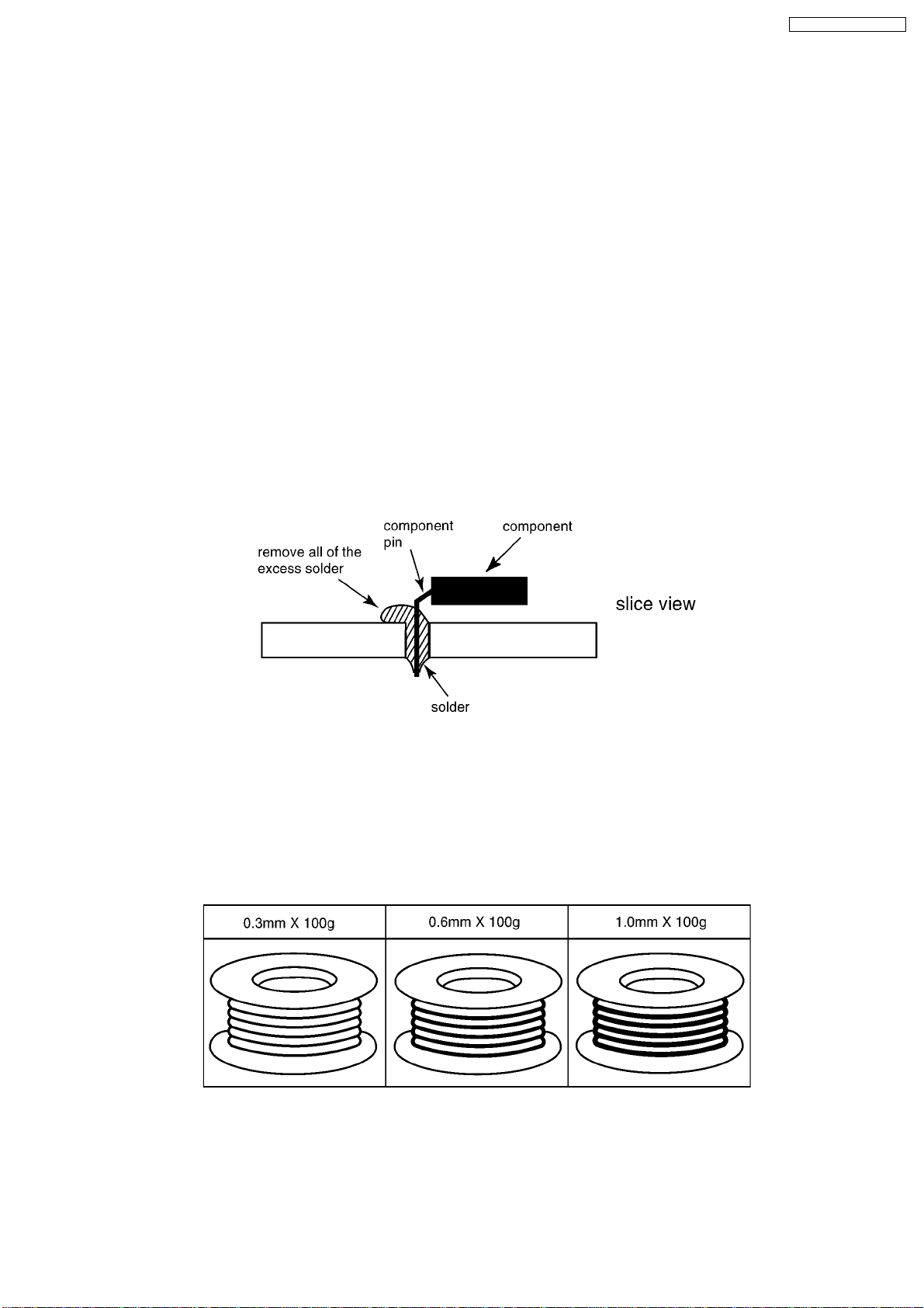
· When applying PbF solder to double layered boards, please check the component side for excess which may flow onto the
opposite side (See figure, below).
1.1. SUGGESTED PbF SOLDER
There are several types of PbF solder available commercially. While this product is manufactured using Tin, Silver, and Copper,
(Sn+Ag+Cu), you can also use Tin and Copper, (Sn+Cu), or Tin, Zinc, and Bismuth, (Sn+Zn+Bi).
Please check the manufacturer’s specific instructions for the melting points of their products and any precautions for using their
product with other materials.
The following lead free (PbF) solder wire gauges are recommended for service of this product: 0.3mm, 0.6mm and 1.0mm.
3
KX-T7665AL / KX-T7665X
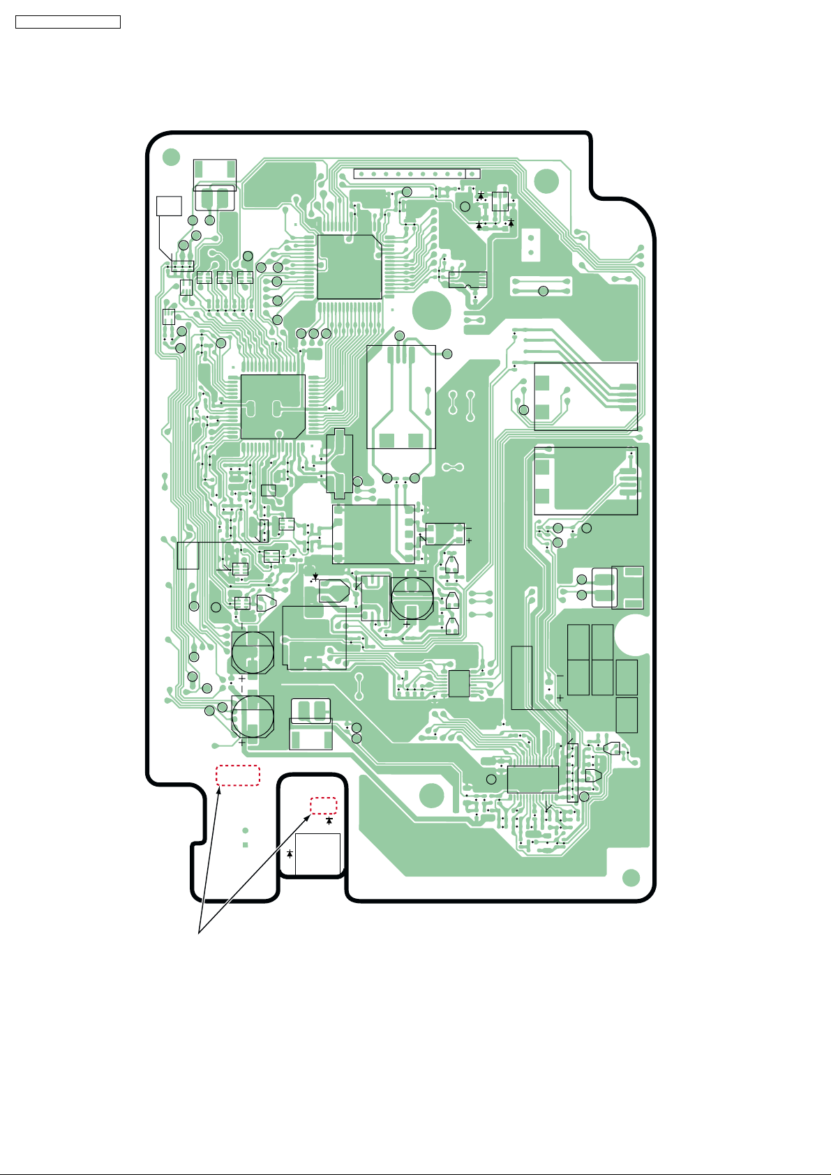
1.2. HOW TO RECOGNIZE THAT Pb FREE SOLDER IS USED
PbF is stamped to show that Pb free solder is used. (See the figure below.)
R
W
R306
A1
R310
Q32
R308
R309
R311
A6
Q31
A3
R307
A4
R516
C104
C103
R100
B3
B2
B1
2
R519
R520
R119
C107
R112
R115
A5
1
B6
A2
Q33 Q34 Q35
R305
R302
R301
R303
R402
PN9
17
R521
R517
R406
R129
C401
32
R116
R114
C101
R113
C108
R110
C105
R109
R111
R117
C106
C114
C120
Q3
R136
R135
Q5
D3V
C117
R200
F5
F7
PSUP1439Z-A
PbF
CN3
B5
E2
R304
R300
R407
16
IC2
33 48
C407
R103
R102
C100
C406
R101
R106
R105
IC7
R108
C102
R107
R104
C113
Q2
R134
R133
R139
R138
Q6
R137
C204
C205
C607
C606
16
17
E1
F8
32 49
F6
33 48
F4
F2
F1
F3
C400
1
64
C403
49
R403
R132
C115
R401
R130
D21
Q21
L21
CN2
R400
C111
C109
C404
C405
R131
5
21
X1
C201
W
C402
Q1
C116
R
PSUP1439Z-B
PbF
D43
10
IC6
D44
B4
R202
R201
C200
C505
R610
1
T1
IC1
R208
R204
AG2
MIC2
R601
C602
64
H
R209
R518
G1
R602
JK1
L1
C203
C202
R526
CN5
C605
T
L
L2
101
9
R206
R515
R604
R603
R611
R609
R608
C118
C112
R524
C110
R207
R525
R600
D5V
D1
R140
R119
R203
R205
C522
R513
R607
R
R114
IC3
C601
IC5
Q4
R142
Q22
Q23
C524
1
C600
C609
GND
R506
R512
C514
R505
D63
D62
C523
C528
C516
C506
R511
IC8
C603
D61
E3
R514
C515
R507
C604
L3
L4
R605
C608
R606
R503
C503
C510
C521
C508
C507
C517
IC4
C519
C502
R502
E4
L51
R527
C518
C511
C520
C512
L52
MIC1
C525
R510
C526
SP1
SPN
SPP
C509
R509
R500
R501
JK2
JK3
C501
RU CNGen
C513
AG1
W
R
R523
R504
C504
R508
A3V
2
1
C527
Q51
C500
CN1
GRA
DB
Q52
R522
Marked PbF
A
KX-T7665AL / KX-T7665X : MAIN BOARD
4

2 FOR SERVICE TECHNICIANS
ICs and LSIs are vulnerable to static electricity.
When repairing, the following precautions will help prevent recurring malfunctions.
1. Cover the plastic parts boxes with aluminum foil.
2. Ground the soldering irons.
3. Use a conductive mat on the worktable.
4. Do not touch IC or LSI pins with bare fingers.
3 SPECIFICATIONS
Station Loop Limit: 90 ohms
Calling Method: 2 pair wire
Jacks: Handset Jack, TEL Jack
Dimensions: Low Angle:
High Angle:
Weight: 0.7 kg
213 (D)mm × 177 (W)mm × 107 (H)mm
201 (D)mm × 177 (W)mm × 127 (H)mm
KX-T7665AL / KX-T7665X
Design and specifications are subject to change without notice.
4 LOCATION OF CONTROLS
5

KX-T7665AL / KX-T7665X
5 CONNECTION
Caution:
The availability of D-XDP function depends on the software version of the connected Business Telephone System.
Consult your dealer for more details about D-XDP.
6
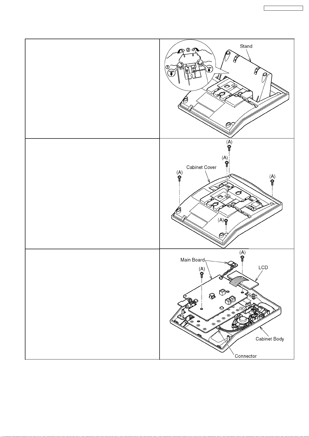
6 DISASSEMBLY INSTRUCTIONS
1. Remove the Stand.
2. Remove 5 Screws (A).
3. Remove the Cabinet Cover.
KX-T7665AL / KX-T7665X
4. Remove the Connector from the Main Board.
5. Remove 2 Screws (A).
6. Remove the Main Board and the LCD from the Cabinet Body.
7
KX-T7665AL / KX-T7665X
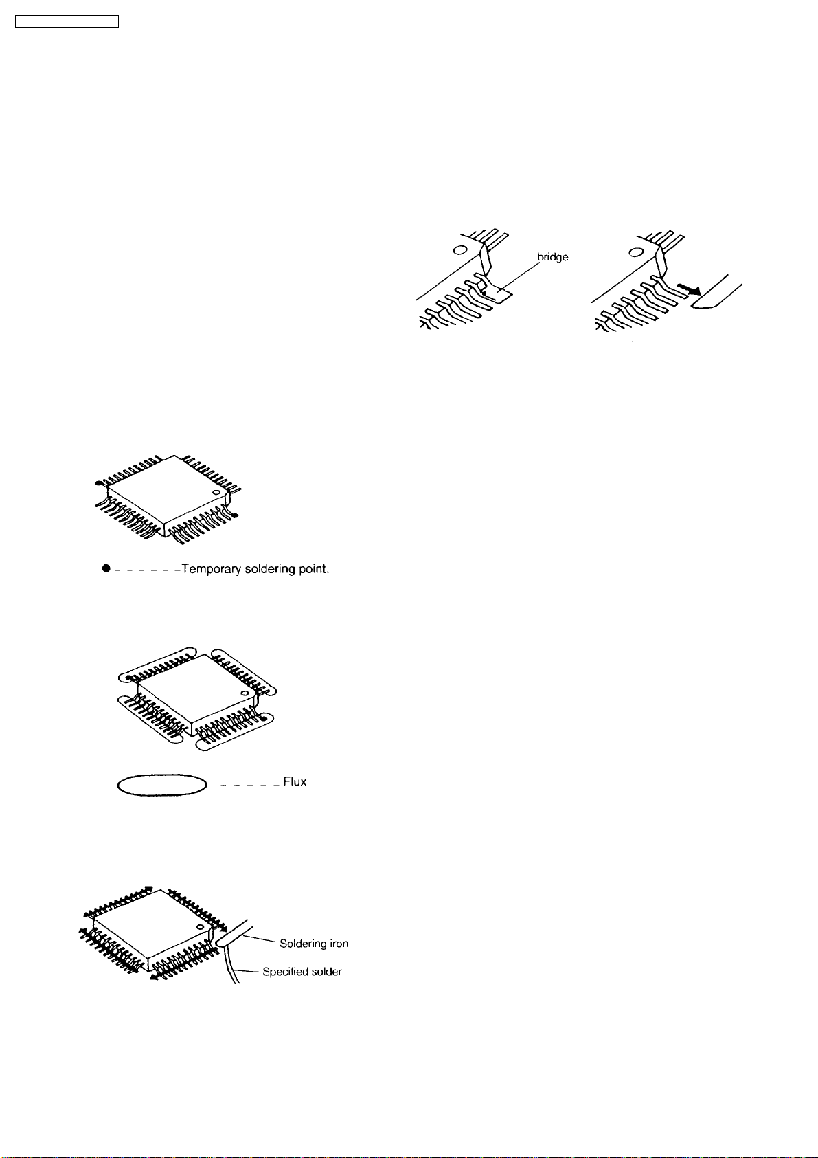
7 HOW TO REPLACE A FLAT PACKAGE IC
7.1. PREPARATION
· PbF (: Pb free) Solder
· Soldering Iron
Tip Temperature of 700°F±20°F (370°C±10°C)
Note: We recommend a 30 to 40 Watt soldering iron. An
expert may be able to use a 60 to 80 Watt iron where
someone with less experience could overheat and damage
the PCB foil.
· Flux
Recommended Flux: Specific Gravity → 0.82.
Type → RMA (lower residue, non-cleaning type)
Note: See ABOUT LEAD FREE SOLDER (PbF: Pb free)
(P.3).
7.2. PROCEDURE
1. Tack the flat pack IC to the PCB by temporarily soldering
two diagonally opposite pins in the correct positions on the
PCB.
7.3. REMOVING SOLDER FROM
BETWEEN PINS
1. Add a small amount of solder to the bridged pins.
2. With a hot iron, use a sweeping motion along the flat part of
the pin to draw the solder from between the adjacent pads.
Be certain each pin is located over the
correct pad on the PCB.
2. Apply flux to all of the pins on the IC.
3. Being careful to not unsolder the tack points, slide the
soldering iron along the tips of the pins while feeding
enough solder to the tip so that it flows under the pins as
they are heated.
8
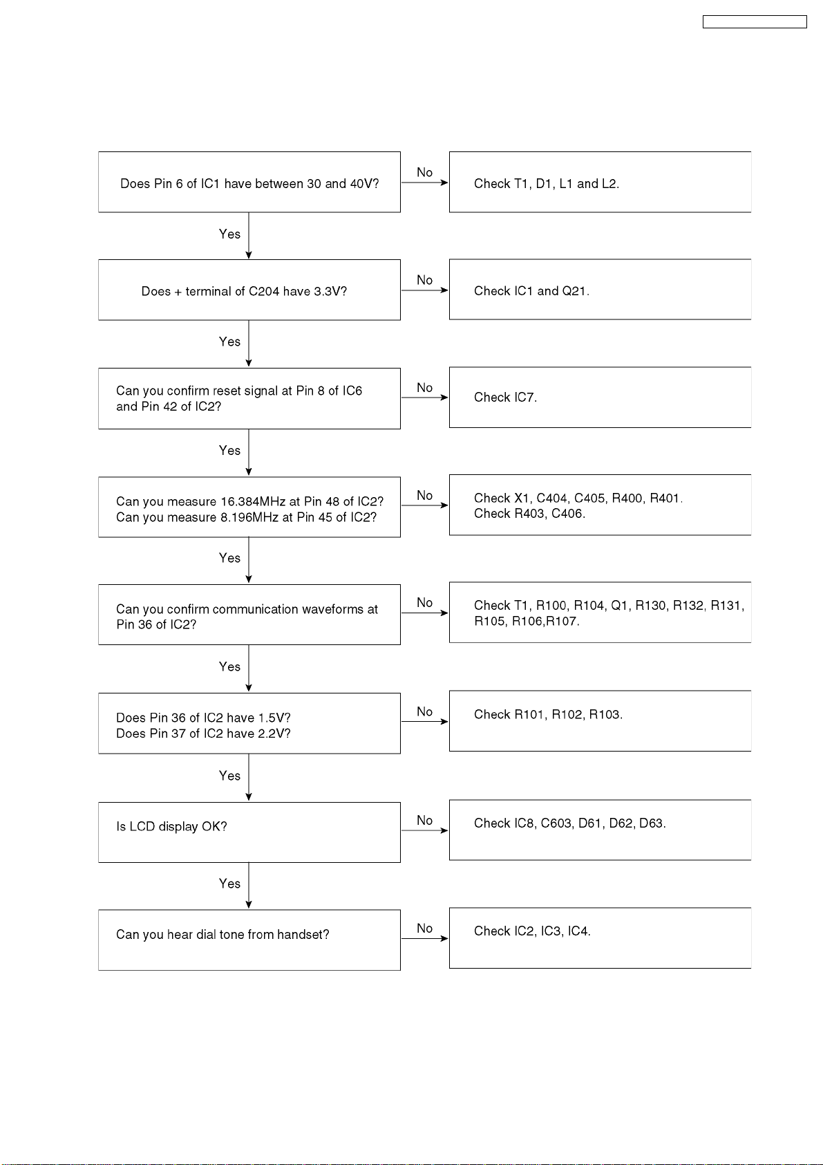
8 TROUBLESHOOTING GUIDE
8.1. NO OPERATION
KX-T7665AL / KX-T7665X
Note:
Refer to (1)~(4) of WAVEFORM (P.34) for waveform.
9
KX-T7665AL / KX-T7665X
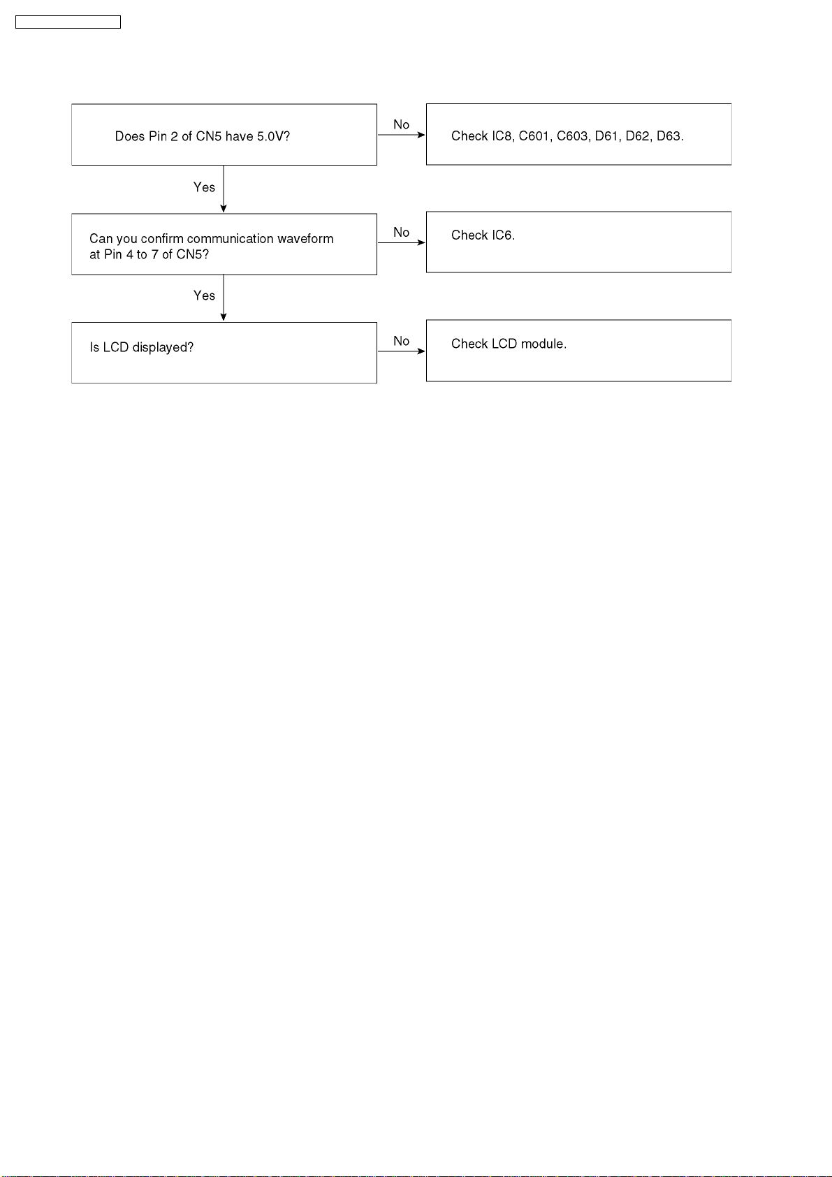
8.2. LCD DOES NOT OPERATE
Note:
Refer to (5)ofWAVEFORM(P.34) for waveform.
10
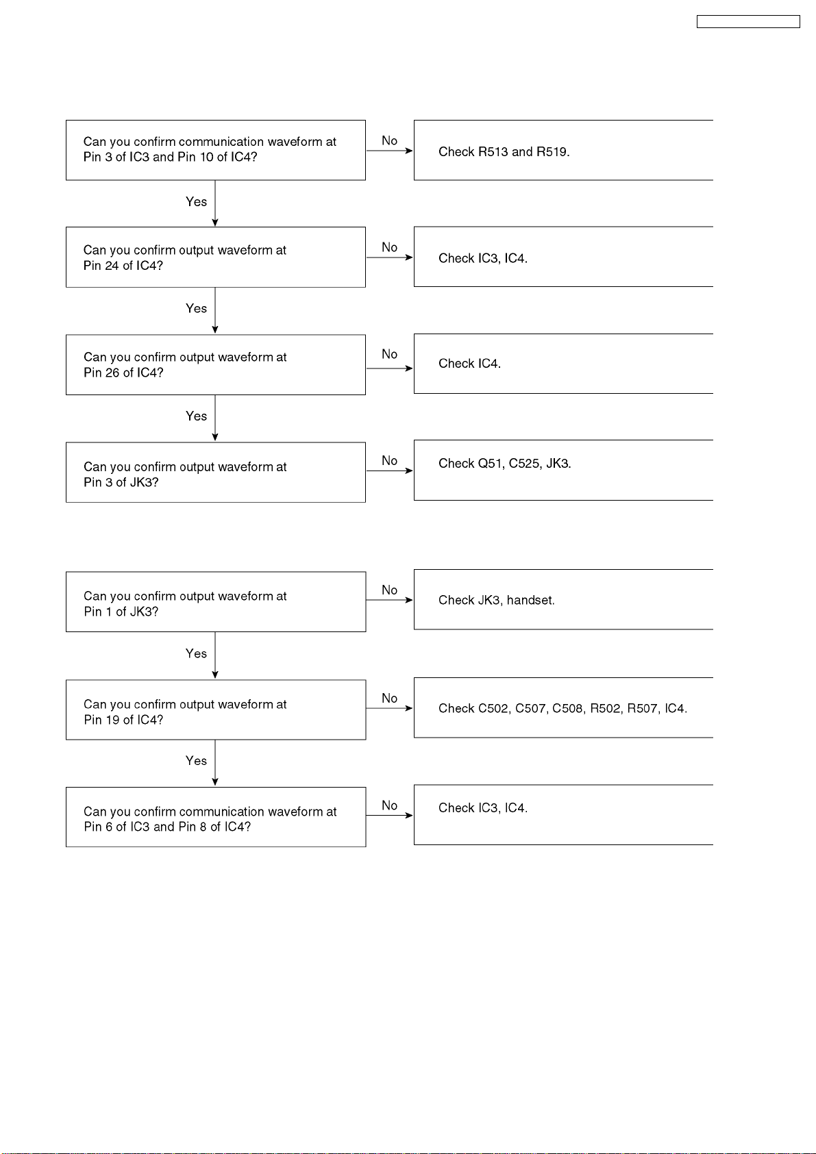
8.3. HANDSET DOES NOT WORK
Receive
KX-T7665AL / KX-T7665X
Send
Note:
Refer to (6)~(7) of WAVEFORM (P.34) for waveform.
11
KX-T7665AL / KX-T7665X
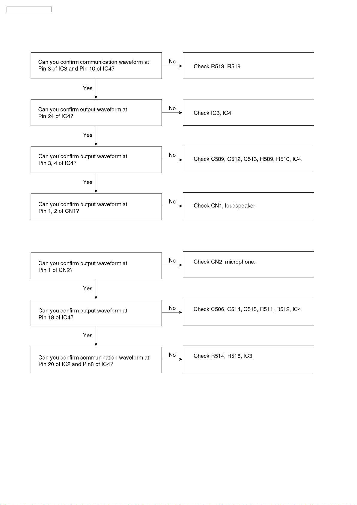
8.4. SPEAKER-PHONE TROUBLE
Receive
Send
Note:
Refer to (6)~(7) of WAVEFORM (P.34) for waveform.
12
 Loading...