


ML9261MB

¡ Semiconductor ML9261/62
1/16
¡ Semiconductor
ML9261/62
60-Bit Vacuum Fluorescent Display Tube Grid/Anode Driver
GENERAL DESCRIPTION
The ML9261/62 is a monolithic IC designed for directly driving the grid and anode of the vacuum
fluorescent display (VFD) tube. The device contains a 60-bit shift register, a 60-bit register circuit,
and 60 VFD tube driving circuits on a single chip.
Display data is serially stored in the shift register at the rising edge of a clock pulse.
Setting the CL pin low allows all the VFD tube driving circuits to be driven low, which makes it
possible to set the display blanking.
Also, setting both of the CL and CHG pins high allows all the VFD tube driving circuits to be
driven high, which provides the easy testing of all lights after final assembly of a VFD tube panel.
FEATURES
• Logic Supply Voltage (V
CC
) : +3.3V±10% or +5.0V±10%
• Driver Supply Voltage (V
HV
): +60V
• Driver Output Current
I
OHVH1
(Only one driver output : "H") : –40mA (V
DISP
=40V)
I
OHVH2
(All the driver outputs : "H") : –120mA (V
DISP
=40V)
I
OHVL
:1mA
• Directly connected to VFD tube by using push-pull output (Pull-down resistors are not
needed)
• Data Transfer Speed: 4MHz
• Package :
70-pin plastic SSOP (SSOP70-P-500-0.80-K) (Product names : ML9261MB and ML9262MB)
E2C0043-19-74
This version: Jul. 1999
Preliminary
¡ Semiconductor ML9261/62
2/16
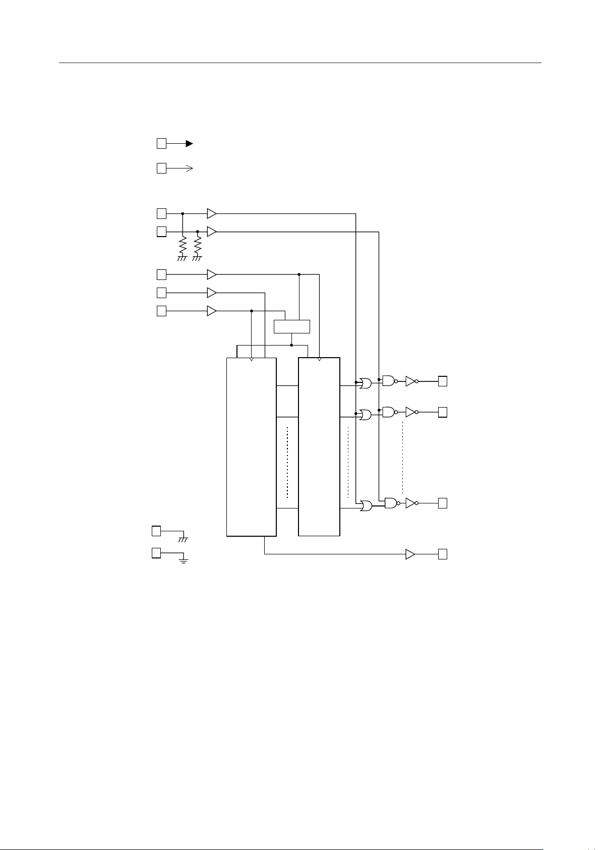
BLOCK DIAGRAM
V
DISP
V
DD
CL
CHG
LS
DIN
CLK
HVO 1
HVO 2HVO
HVO60
DOUT
L-GND
D-GND
CSI
PO-1
PO-2
60-Bit
Shift
Register
60-Bit
Register
P0-60
SO
D-60 O-60
D-2
D-1
O-2
O-1
RESET
RRC

¡ Semiconductor ML9261/62
3/16
INPUT AND OUTPUT CONFIGURATION

¡ Semiconductor ML9261/62
4/16
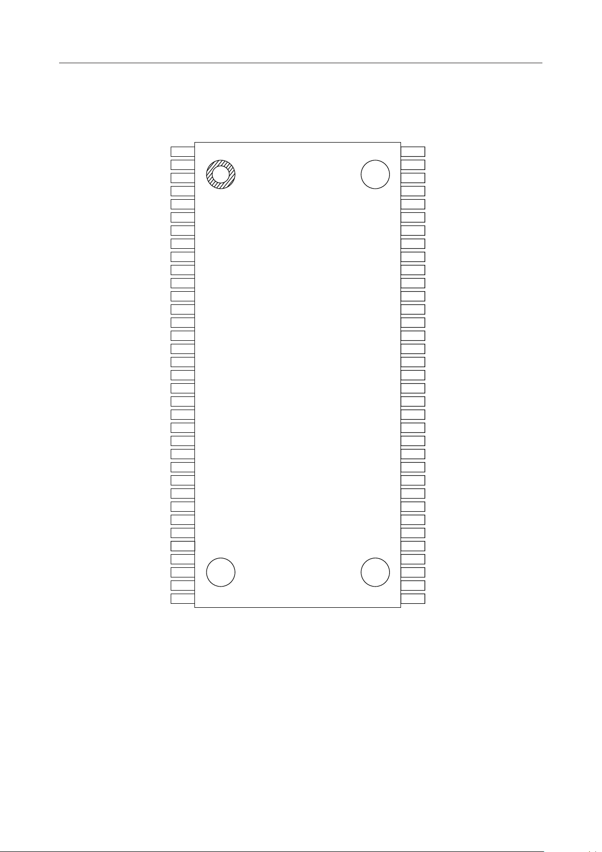
PIN CONFIGURATION (TOP VIEW)
ML9261
1
2
3
4
5
6
7
8
9
10
11
12
13
14
15
16
70
69
68
67
66
65
64
63
62
61
60
59
58
57
56
55
HVO 25
HVO 24
HVO 23
HVO 22
HVO 21
HVO 20
HVO 19
HVO 18
HVO 17
HVO 16
HVO 15
HVO 14
HVO 13
HVO 12
HVO 11
HVO 10
HVO 26
HVO 27
HVO 28
HVO 29
HVO 30
HVO 31
HVO 32
HVO 33
HVO 34
HVO 35
HVO 36
HVO 37
HVO 38
HVO 39
HVO 40
HVO 41
17
18
19
20
54
53
52
51
HVO 9
HVO 8
HVO 7
HVO 6
HVO 42
HVO 43
HVO 44
HVO 45
21
22
23
24
25
26
50
49
48
47
46
45
HVO 5
HVO 4
HVO 3
HVO 2
HVO 1
V
DISP
HVO 46
HVO 47
HVO 48
HVO 49
HVO 50
HVO 51
27
28
29
30
44
43
42
41
V
DD
D
IN
D
OUT
CLK
HVO 52
HVO 53
HVO 54
HVO 55
31 40
LS HVO 56
32
33
34
35
39
38
37
36
CL
CHG
L-GND
D-GND
HVO 57
HVO 58
HVO 59
HVO 60
70-Pin Plastic SSOP
(SSOP70-P-500-0.80-K)
¡ Semiconductor ML9261/62
5/16
1
2
3
4
5
6
7
8
9
10
11
12
13
14
15
16
70
69
68
67
66
65
64
63
62
61
60
59
58
57
56
55
D-GND
L-GND
CHG
CL
LS
CLK
D
OUT
D
IN
V
DD
V
DISP
HVO 1
HVO 2
HVO 3
HVO 4
HVO 5
HVO 6
HVO 60
HVO 59
HVO 58
HVO 57
HVO 56
HVO 55
HVO 54
HVO 53
HVO 52
HVO 51
HVO 50
HVO 49
HVO 48
HVO 47
HVO 46
HVO 45
17
18
19
20
54
53
52
51
HVO 7
HVO 8
HVO 9
HVO 10
HVO 44
HVO 43
HVO 42
HVO 41
21
22
23
24
25
26
50
49
48
47
46
45
HVO 11
HVO 12
HVO 13
HVO 14
HVO 15
HVO 16
HVO 40
HVO 39
HVO 38
HVO 37
HVO 36
HVO 35
27
28
29
30
44
43
42
41
HVO 17
HVO 18
HVO 19
HVO 20
HVO 34
HVO 33
HVO 32
HVO 31
31 40
HVO 21 HVO 30
32
33
34
35
39
38
37
36
HVO 22
HVO 23
HVO 24
HVO 25
HVO 29
HVO 28
HVO 27
HVO 26
70-Pin Plastic SSOP
(SSOP70-P-500-0.80-K)
PIN CONFIGURATION (TOP VIEW)
ML9262
¡ Semiconductor ML9261/62
6/16
PIN DESCRIPTION
Symbol Description
CLK
Shift register clock input pin.
Shift register reads data from DIN while the CLK pin is low and the data in the shift register
is shifted from one stage to the next stage at the rising edge of the clock.
Type
I
Serial data input pin of the shift register.
Display data (positive logic) is input in the DIN pin in synchronization with clock.
DIN
I
Serial data output pin of the shift register.
Data is output from the DOUT pin in synchronization with the CLK signal.
DOUT
O
Latch strobe input pin.
The contents of the parallel outputs (PO1 to PO60) of the shift register are read at the rising
edge of LS (edge-triggered). When the CLK rises while LS is high, the parallel outputs
(PO1 to PO60) and latch outputs (O1 to O60) go low.
LS
I
Clear input pin with a built-in pull-down resistor.
The CL pin is normally set high.
If the CL pin is high and the CHG pin is low, the driver outputs (HV01 to HV60) are in phase
with the corresponding register outputs (O1 to O60).
If the CL pin is high and the CHG pin is high, the driver outputs (HV01 to HV60) are high
irrespective of the states of the register outputs.
If the CL pin is set low, the driver outputs are driven low irrespective of the states of the
CHG pin and register outputs.
This allows display blanking to be set.
CL
I
Input for testing (with a pull-down resistor).
The CL pin is normally set low.
If the CHG pin is low and the CL pin is high, the driver outputs (HV01 to HV60) are in phase
with the corresponding register outputs (O1 to O60).
If the CHG pin is low and the CL pin is low, the driver outputs (HV01 to HV60) are low
irrespective of the states of the register outputs.
If the CHG pin is set high, the driver outputs are driven high irrespective of the states of the
register outputs.
This provides the easy testing of all lights after final assembly.
CHG
I
High voltage driver outputs for driving VFD tube.
If the CL pin is high and the CHG pin is low, the driver outputs are in phase with the
corresponding register outputs (O1 to O60).
The direct connection to the grid or anode of a VFD tube eliminates pull-down resistors.
VHO1-60
O
Power supply pin for driver circuits of VFD tube
V
DISP
Power supply pin for logic
V
DD
GND pin for driver circuits of a VFD tube.
Since the D-GND is not be connected to L-GND, connect this pin to the external L-GND.
D-GND
GND pin for the logic circuits.
Since the L-GND pin is not be connected to D-GND, connect this pin to the external D-GND.
L-GND
 Loading...