


OKI MG75PB34, MG75PB36, MG75PB32, MG75PB38, MG75PB40 Datasheet
...DATA SHEET
O K I A S I C P R O D U C T S
MG113P/114P/115P/73P/74P/75P
0.25µm Sea of Gates and
Customer Structured Arrays
November 1999

■ ■ ––––––––––––––––––––––––––––––––––––––––––––––––––––––––
Oki Semiconductor

MG113P/114P/115P/73P/74P/75P
0.25µm Sea of Gates and Customer Structured Arrays
DESCRIPTION
Oki’s 0.25µm Application-Specific Integrated Circuit (ASIC) products are available in both Sea Of Gates (SOG) and Customer Structured Array (CSA) architectures. Both the SOG-based MG115P series and the CSA-based MG75P series use a five-layer metal process on 0.25µm drawn (0.18µm L-effective) CMOS technology. The SOG MG113P/114P series uses the same SOG base-array architecture as the MG115P series, but offers four and three metal layers, respectively. The MG73P/74P CSA series uses three and four metal layers, respectively. The semiconductor process is adapted from Oki’s production-proven 64Mbit DRAM manufacturing process.
The 0.25µm family provides significant performance, density, and power improvement over previous 0.30 and 0.35µm technologies. An innovative 4-transistor cell structure, licensed from In-Chip Systems, Inc., provides 30 to 50% less power and 30 to 50% more usable gates than traditional cell designs. The Oki 0.25µm family operates using 2.5-V VDD core with optimized 3-V I/O buffers. The 3-, 4-, and 5-layer metal MG113P/114P/115P SOG series contains 4 array bases, offering up to 588 I/O pads and over 2.4M raw gates. The 3-, 4-, and 5-layer metal MG73P/74P/75P CSA series contains 21 array bases, offering up to 868 I/O pads and over 5.4M raw gates. These SOG and CSA array sizes are designed to fit the most popular quad flat pack (QFP), low profile QFPs (LQFPs), thin QFPs (TQFPs), and plastic ball grid array (PBGA) packages.
The MG113P/114P/115P series SOG architecture allows rapid prototyping turnaround times (TATs), additionally offering the most cost-effective solution for pad-limited circuits (particularly the 3-layer metal MG113P series). The 3-layer-metal MG73P, 4-layer-metal MG74P and 5-layer-metal MG75P CSA series contains 21 array bases, offering a wider span of gate and I/O counts than the SOG series. Oki uses the Artisan Components memory compiler which provides high performance, embedded synchronous singleand dual-port RAM macrocells for CSA designs. As such, the MG73P/74P/75P series is suited to memory-intensive ASICs and high-volume designs where fine tuning of package size produces significant cost or real-estate savings.
Oki Semiconductor |
1 |

■ MG113P/114P/115P/73P/74P/75P ■ –––––––––––––––––––––––––––––––––––––––––
FEATURES
•0.25µm drawn 3-, 4-, and 5-layer metal CMOS
•Optimized 2.5-V core
•Optimized 3-V I/O
•SOG and CSA architecture availability
•77-ps typical gate propagation delay (for a 4xdrive inverter gate with a fanout of 2 and 0 mm of wire, operating at 2.5 V)
•Over 5.4M raw gates and 868 I/O pads using 60µ staggered I/O
•User-configurable I/O with VSS, VDD, TTL, 3-state, and 1- to 24-mA options
•Slew-rate-controlled outputs for low-radiated noise
•H-clock tree cells which reduces the maximum skew for clock signals
•Low 0.2µW/MHz/gate power dissipation
•User-configurable singleand dual-port memories
•Specialized IP cores and macrocells including 32-bit ARM7TDMI CPU, phase-locked loop (PLL), and peripheral component interconnect (PCI) cells
•Floorplanning for front-end simulation, backend layout controls, and link to synthesis
•Joint Test Action Group (JTAG) boundary scan and scan path Automatic Test Pattern Generation (ATPG)
•Support for popular CAE systems including Cadence, IKOS, Mentor Graphics, Model Technology, Inc. (MTI), Synopsys, and Viewlogic
2 |
Oki Semiconductor |

–––––––––––––––––––––––––––––––––––––––––––––––––––––––––■ MG113P/114P/115P/73P/74P/75P ■
MG113P/114P/115P/73P/74P/75P FAMILY LISTING
|
60µm Staggered PAD products |
|
|
|
|
|
||
|
|
|
|
|
No. of |
MG113P/73P |
MG114P/74P |
MG115P/75P |
|
|
No. of |
No. of |
No. of |
Raw |
Family 3LM |
Family 4LM |
Family 5LM |
SOG Base Array |
EA Base Array |
Pads |
Rows |
Columns |
Gates |
Usable Gates |
Usable Gates |
Usable Gates |
|
MG7xPB02 |
68 |
84 |
280 |
23,520 |
|
22,344 |
22,344 |
|
|
|
|
|
|
|
|
|
|
MG7xPB04 |
108 |
144 |
480 |
69,120 |
|
65,664 |
65,664 |
|
|
|
|
|
|
|
|
|
|
MG7xPB06 |
148 |
204 |
680 |
138,720 |
|
131,784 |
131,784 |
|
|
|
|
|
|
|
|
|
|
MG7xPB08 |
188 |
264 |
880 |
232,320 |
|
218,381 |
220,704 |
|
|
|
|
|
|
|
|
|
|
MG7xPB10 |
228 |
324 |
1,080 |
349,920 |
|
311,429 |
332,424 |
|
|
|
|
|
|
|
|
|
|
MG7xPB12 |
268 |
384 |
1,280 |
491,520 |
|
412,877 |
466,944 |
|
|
|
|
|
|
|
|
|
MG11xP14 |
MG7xPB14 |
308 |
444 |
1,480 |
657,120 |
387,701 |
519,125 |
611,122 |
|
|
|
|
|
|
|
|
|
|
MG7xPB16 |
348 |
504 |
1,680 |
846,720 |
|
635,040 |
745,114 |
|
|
|
|
|
|
|
|
|
MG11xP18 |
MG7xPB18 |
388 |
564 |
1,880 |
1,060,320 |
572,573 |
763,430 |
901,272 |
|
|
|
|
|
|
|
|
|
|
MG7xPB20 |
428 |
624 |
2,080 |
1,297,920 |
|
882,586 |
1,025,357 |
|
|
|
|
|
|
|
|
|
MG11xP22 |
MG7xPB22 |
468 |
684 |
2,280 |
1,559,920 |
732,974 |
982,498 |
1,154,045 |
|
|
|
|
|
|
|
|
|
|
MG7xPB24 |
508 |
744 |
2,480 |
1,845,120 |
|
1,107,072 |
1,310,035 |
|
|
|
|
|
|
|
|
|
|
MG7xPB26 |
548 |
804 |
2,680 |
2,154,720 |
|
1,249,738 |
1,465,210 |
|
|
|
|
|
|
|
|
|
MG11xP28 |
MG7xPB28 |
588 |
864 |
2,880 |
2,488,320 |
1,094,861 |
1,393,459 |
1,642,291 |
|
|
|
|
|
|
|
|
|
|
MG7xPB30 |
628 |
924 |
3,080 |
2,845,920 |
|
1,536,797 |
1,821,389 |
|
|
|
|
|
|
|
|
|
|
MG7xPB32 |
668 |
984 |
3,280 |
3,227,520 |
|
1,678,310 |
2,001,062 |
|
|
|
|
|
|
|
|
|
|
MG7xPB34 |
708 |
1,044 |
3,480 |
3,633,120 |
|
1,816,560 |
2,179,872 |
|
|
|
|
|
|
|
|
|
|
MG7xPB36 |
748 |
1,104 |
3,680 |
4,062,720 |
|
1,950,106 |
2,356,378 |
|
|
|
|
|
|
|
|
|
|
MG7xPB38 |
788 |
1,164 |
3,880 |
4,516,320 |
|
2,077,507 |
2,529,139 |
|
|
|
|
|
|
|
|
|
|
MG7xPB40 |
828 |
1,224 |
4,080 |
4,993,920 |
|
2,197,325 |
2,696,717 |
|
|
|
|
|
|
|
|
|
|
MG7xPB42 |
868 |
1,284 |
4,280 |
5,495,520 |
|
2,308,118 |
2,857,670 |
|
|
|
|
|
|
|
|
|
ARRAY ARCHITECTURE
The primary components of a 0.25µm MG113P/114P/115P circuit include:
•I/O base cells
•60µm pad pitch
•Configurable I/O pads for VDD, VSS, or I/O (optimized 3-V I/O)
•VDD and VSS pads dedicated to wafer probing
•Separate power bus for output buffers
•Separate power bus for internal core logic and input buffers
•Core base cells containing N-channel and P-channel pairs, arranged in column of gates
•Isolated gate structure for reduced input capacitance and increased routing flexibility
•Innovative 4-transistor core cell architecture, licensed from In-Chip Systems, Inc
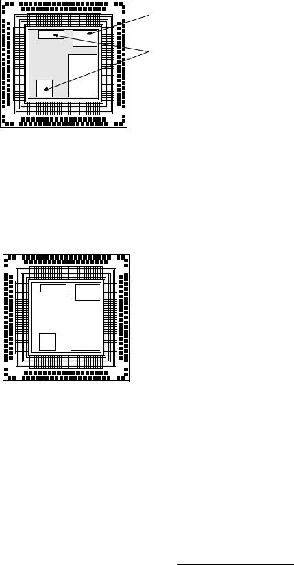
Each array has 24 dedicated corner pads for power and ground use during wafer probing, with four pads per corner. The arrays also have separate power rings for the internal core functions (VDDC and VSSC) and output drive transistors (VDDO and VSSO).
Oki Semiconductor |
3 |

■ MG113P/114P/115P/73P/74P/75P ■ –––––––––––––––––––––––––––––––––––––––––
I/O base cells |
Separate power bus (VDDC, VSSC) for |
internal core logic (2nd metal/3rd metal) |
Configurable I/O pads for VDD, VSS, or I/O
1, 2, 3, 4, or 5 layer metal interconnection in core area
Core base cell with 4 transistors
VDD, VSS pads (4) in each corner for wafer probing only
Separate power bus (VDDO, VSSO) over I/O cell for output buffers (2nd metal/3rd metal)
Figure 7. MG115P Array Architecture
MG73P/74P/75P CSA Layout Methodology
The procedure to design, place, and route a CSA follows.
1.Select suitable base array frame from the available predefined sizes. To select an array size:
-Identify macrocell functions required and minimum array size to hold macrocell functions.
-Add together all the area occupied by the required random logic and macrocells and select the optimum array.
2.Make a floor plan for the design’s megacells.
-Oki Design Center engineers verify the master slice and review simulation.
-Oki Design Center or customer engineers floorplan the array using Oki’s supported floorplanner or Cadence DP3 or Gambit GFP and customer performance specifications.
-Using Oki CAD software, Design Center engineers remove the SOG transistors and replace them with diffused memory macrocells to the customer’s specifications.
4 |
Oki Semiconductor |
–––––––––––––––––––––––––––––––––––––––––––––––––––––––––■ MG113P/114P/115P/73P/74P/75P ■
Figure 8 shows an array base after placement of the optimized memory macrocells.
High-density RAM
Mega macrocells
Figure 8. Optimized Memory Macrocell Floor Plan
3. Place and route logic into the array transistors.
-Oki Design Center engineers use layout software and customer performance specifications to connect the random logic and optimized memory macrocells.
Figure 9 marks the area in which placement and routing is performed with cross hatching.
Figure 9. Random Logic Place and Route
Oki Semiconductor |
5 |
 Loading...