


OKI MG65PB40, MG65PB38, MG65PB34, MG65PB32, MG65PB12 Datasheet
...DATA SHEET
O K I A S I C P R O D U C T S
MG63P/64P/65P
0.25µm Embedded DRAM/
Customer Structured Arrays
November 1998

MG63P/64P/65P
0.25µm Embedded DRAM/Customer Structured Arrays
DESCRIPTION
Oki’s 0.25 µm MG63P/64P/65P Application-Specific Integrated Circuit (ASIC) provides the ability to embed large blocks of Synchronous DRAM (SDRAM) into an embedded array architecture called the Customer Structured Array (CSA). Utilizing Oki’s leadership in DRAM technologies and wide experience of embedding SDRAM in logic products, Oki is able to integrate SDRAM and ASIC technology. The merged DRAM/ASIC process efficiently implements the Oki stacked capacitor memory cell. The MG63P/64P/65P CSA series uses three, four, and five metal process layers, respectively, on 0.25 µm drawn (0.18 µm L-effective) CMOS technology. The semiconductor process is adapted from Oki’s pro- duction-proven 64Mbit DRAM manufacturing process.
The 0.25 µm family provides significant performance, density, and power improvement over previous 0.30 µm and 0.35 µm technologies. An innovative 4-transistor cell structure provides 30 to 50% less power and 30 to 50% more usable gates than traditional cell designs. The Oki 0.25 µm family operates using 2.5-V VDD core with optimized 3-V I/O buffers. The 3-, 4-, and 5-layer metal MG63P/64P/65P CSA series contains 21 devices each, offering up to 868 I/O pads and over 5.4M raw gates. These CSA array sizes are designed to fit the most popular quad flat pack (QFP), low profile QFPs (LQFPs), thin QFPs (TQFPs), and plastic ball grid array (PBGA) packages. Oki uses the Artisan Components memory compiler which provides high performance, embedded synchronous singleand dual-port SRAM macrocells for CSA designs. As such, the MG63P/64P/65P series is suited to memory-intensive ASICs and high volume designs where fine tuning of package size produces significant cost or real-estate savings.
The embedded SDRAM represents part of Oki’s menu of major IP core functions for the 0.25 µm ASIC products. Other functions include ARM7TDMI, Gb Ethernet MAC, PLL, PCI and others in planning.
FEATURES
•0.25µm drawn 3-, 4-, and 5-layer metal CMOS
•Optimized 2.5-V core
•Optimized 3-V I/O
•CSA architecture availability
•100 MHz embedded SDRAM cores up to 16 Mb per occurrence
•77-ps typical logic gate propagation delay (for a 4x-drive inverter gate with a fanout of 2 and 0 mm of wire, operating at 2.5 V)
•Over 5.4M raw gates and 868 I/O pads using 60µ staggered I/O
•User-configurable I/O with VSS, VDD, TTL, 3-state, and 1- to 24-mA options
•Slew-rate-controlled outputs for low-radiated noise
•H-clock tree cells which reduces the maximum skew for clock signals
•Low 0.2µW/MHz/gate power dissipation
•User-configurable singleand dual-port memories (SRAM)
•Specialized IP cores and macrocells including 32-bit ARM7TDMI CPU, phase-locked loop (PLL), and peripheral component interconnect (PCI) cells
•Floorplanning for front-end simulation, backend layout controls, and link to synthesis
•Joint Test Action Group (JTAG) boundary scan and scan path Automatic Test Pattern Generation (ATPG)
•Support for popular CAE systems including Cadence, IKOS, Mentor Graphics, Model Technology, Inc. (MTI), Synopsys, and Viewlogic
Oki Semiconductor |
1 |

■ MG63P/64P/65P ■ –––––––––––––––––––––––––––––––––––––––––––––––––
MG63P/64P/65P FAMILY LISTING
|
No. of |
No. of |
No. of |
No. of Raw |
MG63P 3LM |
MG64P 4LM |
MG65P 5LM |
Series (MG6x) |
Pads |
Rows |
Columns |
Gates |
Usable Gates |
Usable Gates |
Usable Gates |
B02 |
68 |
84 |
280 |
23,520 |
20,933 |
22,344 |
22,344 |
|
|
|
|
|
|
|
|
B04 |
108 |
144 |
480 |
69,120 |
57,370 |
65,664 |
65,664 |
|
|
|
|
|
|
|
|
B06 |
148 |
204 |
680 |
138,720 |
106,814 |
131,784 |
131,784 |
|
|
|
|
|
|
|
|
B08 |
188 |
264 |
880 |
232,320 |
167,270 |
218,381 |
220,704 |
|
|
|
|
|
|
|
|
B10 |
228 |
324 |
1,080 |
349,920 |
234,446 |
311,429 |
332,424 |
|
|
|
|
|
|
|
|
B12 |
268 |
384 |
1,280 |
491,520 |
309,658 |
412,877 |
466,944 |
|
|
|
|
|
|
|
|
B14 |
308 |
444 |
1,480 |
657,120 |
387,701 |
519,125 |
611,122 |
|
|
|
|
|
|
|
|
B16 |
348 |
504 |
1,680 |
846,720 |
474,163 |
635,040 |
745,114 |
|
|
|
|
|
|
|
|
B18 |
388 |
564 |
1,880 |
1,060,320 |
572,573 |
763,430 |
901,272 |
|
|
|
|
|
|
|
|
B20 |
428 |
624 |
2,080 |
1,297,920 |
648,960 |
882,586 |
1,025,357 |
|
|
|
|
|
|
|
|
B22 |
468 |
684 |
2,280 |
1,559,920 |
732,974 |
982,498 |
1,154,045 |
|
|
|
|
|
|
|
|
B24 |
508 |
744 |
2,480 |
1,845,120 |
848,755 |
1,107,072 |
1,310,035 |
|
|
|
|
|
|
|
|
B26 |
548 |
804 |
2,680 |
2,154,720 |
969,624 |
1,249,738 |
1,465,210 |
|
|
|
|
|
|
|
|
B28 |
588 |
864 |
2,880 |
2,488,320 |
1,094,861 |
1,393,459 |
1,642,291 |
|
|
|
|
|
|
|
|
B30 |
628 |
924 |
3,080 |
2,845,920 |
1,223,746 |
1,536,797 |
1,821,389 |
|
|
|
|
|
|
|
|
B32 |
668 |
984 |
3,280 |
3,227,520 |
1,355,558 |
1,678,310 |
2,001,062 |
|
|
|
|
|
|
|
|
B34 |
708 |
1,044 |
3,480 |
3,633,120 |
1,489,579 |
1,816,560 |
2,179,872 |
|
|
|
|
|
|
|
|
B36 |
748 |
1,104 |
3,680 |
4,062,720 |
1,625,088 |
1,950,106 |
2,356,378 |
|
|
|
|
|
|
|
|
B38 |
788 |
1,164 |
3,880 |
4,516,320 |
1,761,365 |
2,077,507 |
2,529,139 |
|
|
|
|
|
|
|
|
B40 |
828 |
1,224 |
4,080 |
4,993,920 |
1,897,690 |
2,197,325 |
2,696,717 |
|
|
|
|
|
|
|
|
B42 |
868 |
1,284 |
4,280 |
5,495,520 |
2,033,342 |
2,308,118 |
2,857,670 |
|
|
|
|
|
|
|
|
5 layer metal: MG65PBxx
4 layer metal: MG64PBxx
3 layer metal: MG63PBxx
ARRAY ARCHITECTURE
The primary components of a 0.25µm MG63P/64P/65P circuit include:
•I/O base cells
•60µm pad pitch
•Configurable I/O pads for VDD, VSS, or I/O (optimized 3-V I/O)
•VDD and VSS pads dedicated to wafer probing
•Separate power bus for output buffers
•Separate power bus for internal core logic and input buffers
•Core base cells containing N-channel and P-channel pairs, arranged in column of gates
•Isolated gate structure for reduced input capacitance and increased routing flexibility
Each array has 24 dedicated corner pads for power and ground use during wafer probing, with four pads per corner. The arrays also have separate power rings for the internal core functions (VDDC and VSSC) and output drive transistors (VDDO and VSSO).
2 |
Oki Semiconductor |

–––––––––––––––––––––––––––––––––––––––––––––––––––––––––■ MG63P/64P/65P ■
I/O base cells |
Separate power bus (VDDC, VSSC) for |
internal core logic (2nd metal/3rd metal) |
Configurable I/O pads for VDD, VSS, or I/O
1, 2, 3, 4, or 5 layer metal interconnection in core area
Core base cell with 4 transistors
VDD, VSS pads (4) in each corner for wafer probing only
Separate power bus (VDDO, VSSO) over I/O cell for output buffers (2nd metal/3rd metal)
Figure 7. MG65P Array Architecture
MG63P/64P/65P CSA Layout Methodology
The procedure to design, place, and route a CSA follows.
1.Select suitable base array frame from the available predefined sizes. To select an array size:
-Identify megacell functions (e.g. embedded SDRAM) required and minimum array size to hold macrocell functions.
-Add together all the area occupied by the required random logic and macrocells and select the optimum array.
2.Make a floor plan for the design’s megacells.
-Oki Design Center engineers verify the master slice and review simulation.
-Oki Design Center or customer engineers floorplan the array using Oki’s supported Cadence DP3 or Gambit GFP and customer performance specifications.
-Using Oki CAD software, Design Center engineers remove the SOG transistors and replace them with diffused memory macrocells to the customer’s specifications.
Oki Semiconductor |
3 |
■ MG63P/64P/65P ■ –––––––––––––––––––––––––––––––––––––––––––––––––
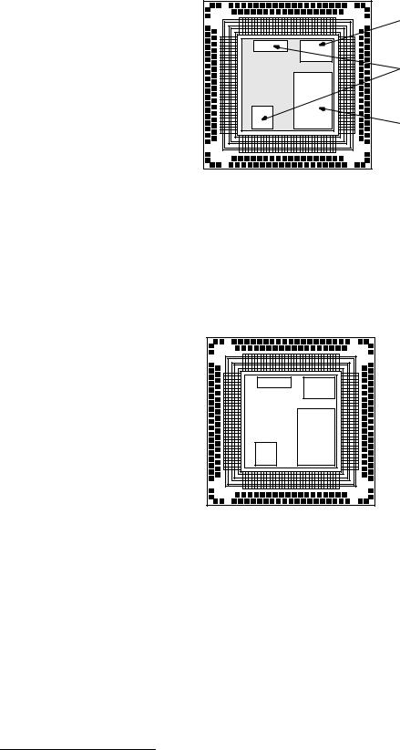
Figure 8 shows an array base after placement of the optimized memory macrocells.
High-density SRAM
Mega macrocells |
Embedded SDRAM |
Figure 8. Optimized Memory Macrocell Floor Plan
3. Place and route logic into the array transistors.
-Oki Design Center engineers use layout software and customer performance specifications to connect the random logic and optimized memory macrocells.
Figure 9 marks the area in which placement and routing is performed with cross hatching.
Figure 9. Random Logic Place and Route
Figure 10 illustrates Oki’s Embedded DRAM ASIC. Oki provides two types of reconfigurable SDRAM cores generated from the compiler.
4 |
Oki Semiconductor |

–––––––––––––––––––––––––––––––––––––––––––––––––––––––––■ MG63P/64P/65P ■
Reconfigurable SDRAM Core
|
|
|
|
|
|
|
|
|
|
|
|
|
|
Data Input |
|
|
|
|
|
|
|
|
|
|
|
|
|
|
|
|
|
|
|
|
|
|
|
|
|
|
|
|
|
|
|
(128 bit) |
|
|
Control |
|
Bank(512Kb) |
|
Bank(512Kb) |
|
|
|
Bank(512Kb) |
|
I/O |
|
|
|
|
|
|
|
|
|
|
|
|
|
Data Output |
|
|||||
|
|
|
|||||||||||||
|
|
|
|
|
|
|
|
|
|
|
|
|
|
|
|
|
|
|
|
|
|
|
|
|
|
|
|
|
|
(128 bit) |
|
|
|
|
|
|
|
|
|
|
|
|
|
|
|
|
|
|
|
|
|
|
|
|
|
|
|
|
|
|
|
|
|
|
|
|
|
|
|
|
|
|
|
|
|
|
|
|
|
Type I: 512 Kb (1 bank) - 8 Mb (16 bank); 512 Kb increment
|
|
|
|
|
|
|
|
|
|
|
|
|
|
Data Input |
|
|
|
|
|
|
|
|
|
|
|
|
|
|
|
|
|
|
|
|
|
|
|
|
|
|
|
|
|
|
|
(256 bit) |
|
|
Control |
|
Bank(1Mb) |
|
Bank(1Mb) |
|
|
|
Bank(1Mb) |
|
I/O |
|
|
|
|
|
|
|
|
|
|
|
|
|
Data Output |
|
|||||
|
|
|
|||||||||||||
|
|
|
|
|
|
|
|
|
|
|
|
|
|
|
|
|
|
|
|
|
|
|
|
|
|
|
|
|
|
(256 bit) |
|
|
|
|
|
|
|
|
|
|
|
|
|
|
|
|
|
|
|
|
|
|
|
|
|
|
|
|
|
|
|
|
|
|
|
|
|
|
|
|
|
|
|
|
|
|
|
|
|
Type I I: 1Mb (1 bank) - 16 Mb (16 bank); 1Mb increment |
|
|
Figure 10. SDRAM Compiler |
SDRAM Core Functional Specification |
|
|
|
Density |
Type I: 512kb (1BK) - 8Mb (16BK) by 512 kb |
|
Type II: 1 Mb (1BK) - 16 Mb (16 BK) by 1 Mb |
|
|
Bit Organization |
x16/x32/x64/x128/x256 (x256 Type II Only) |
|
|
Maximum Clock Rate |
100 MHz |
|
|
VDD |
2.5V |
|
|
CAS Latency |
2 |
|
|
Burst Length |
1 |
|
|
Write Latency |
0 |
|
|
DQM Latency |
0: Write, 2: Read |
|
|
Refresh |
512 Refresh cycles/8 ms |
|
|
Macro Pinout |
CLK, ACT, PRE, RD, WR, AX(8:0), AY(2:0), BAX(2:0), BAY(2:0), DQM (15:0), D(127:0), |
|
Q9127:0), REF, RST, test pins |
|
|
Oki Semiconductor |
5 |
 Loading...