


KDADV-5500-J
Table of contents
 Loading...
JVC KDADV-5500-J, KDADV-5580-J, KDDV-4504-UI, KDDV-4505-A, KDDV-4505-UH Service manual
...
SERVICE MANUAL
COPYRIGHT © 2009 Victor Company of Japan, Limited
No.MA437<Rev.003>
2009/11
DVD/CD RECEIVER
MA437<Rev.003>200911SERVICE MANUAL
KD-ADV5580J, KD-DV5500J, KD-DV4504UI,
KD-DV4505U, KD-DV4505UN, KD-DV4505UT,
KD-DV4505A, KD-DV4506U, KD-DV4506UN,
KD-DV4506UT, KD-DV4506A, KD-DV4588UF,
KD-DV4505UH, KD-DV4506UH
COPYRIGHT © 2009 Victor Company of Japan, Limited
Lead free solder used in the board (material : Sn-Ag-Cu, melting point : 219 Centigrade)
Lead free solder used in the board (material : Sn-Cu, melting point : 230 Centigrade)
TABLE OF CONTENTS
1 PRECAUTION. . . . . . . . . . . . . . . . . . . . . . . . . . . . . . . . . . . . . . . . . . . . . . . . . . . . . . . . . . . . . . . . . . . . . . . . . 1-6
2 SPECIFIC SERVICE INSTRUCTIONS. . . . . . . . . . . . . . . . . . . . . . . . . . . . . . . . . . . . . . . . . . . . . . . . . . . . . . 1-9
3 DISASSEMBLY . . . . . . . . . . . . . . . . . . . . . . . . . . . . . . . . . . . . . . . . . . . . . . . . . . . . . . . . . . . . . . . . . . . . . . 1-10
4 ADJUSTMENT . . . . . . . . . . . . . . . . . . . . . . . . . . . . . . . . . . . . . . . . . . . . . . . . . . . . . . . . . . . . . . . . . . . . . . . 1-16
5 TROUBLESHOOTING . . . . . . . . . . . . . . . . . . . . . . . . . . . . . . . . . . . . . . . . . . . . . . . . . . . . . . . . . . . . . . . . . 1-20
KD-ADV5580/KD-DV5500
KD-DV4506
KD-DV4505
KD-DV4504
1-2 (No.MA437<Rev.003>)
SPECIFICATION
KD-ADV5580/KD-DV5500
AUDIO AMPLIFIER SECTION
Power Output
20 W RMS × 4 Channels at 4 Ω and < or = 1% THD+N
Signal-to-Noise Ratio 80 dBA (reference: 1 W into 4 Ω)
Load Impedance 4 Ω (4 Ω to 8 Ω allowance)
Tone Control Range Bass ±12 dB (60 Hz, 80 Hz, 100 Hz, 120 Hz) Q0.5, Q1.0, Q1.5, Q2.0
Middle ±12 dB (60 Hz, 80 Hz, 100 Hz, 120 Hz) Q0.5, Q1.0, Q1.5, Q2.0
Treble ±12 dB (7.5 kHz, 10.0 kHz, 12.5 kHz, 15.0 kHz) Q0.75, Q1.25
Audio Output Level Digital (DIGITAL OUT: Optical) Signal wave length: 660 nm
Output level: -21 dBm to -15 dBm
Line-Out Level/Impedance KD-ADV5580: 5.0 V/20 kΩ load (full scale)
KD-DV5500: 2.5 V/20 kΩ load (full scale)
Output Impedance 1 kΩ
Color System NTSC
Video Output (composite) 1 Vp-p/75 Ω
Other Terminal AUX (auxiliary) input jack, CD changer jack, Steering wheel remote input (for KD-ADV5580)
TUNER SECTION
Frequency Range FM with channel interval set to 100 kHz or 200 kHz 87.5 MHz to 107.9 MHz
with channel interval set to 50 kHz 87.5 MHz to 108.0 MHz
AM with channel interval set to 10 kHz 530 kHz to 1 710 kHz
with channel interval set to 9 kHz 531 kHz to 1 602 kHz
FM Tuner Usable Sensitivity 9.3 dBf (0.8 µV/75 Ω)
50 dB Quieting Sensitivity 16.3 dBf (1.8 µV/75 Ω)
Alternate Channel Selectivity (400 kHz) 65 dB
Frequency Response 40 Hz to 15 000 Hz
Stereo Separation 40 dB
AM Tuner Sensitivity 20 µV
Sensitivity 40 dB
DVD/CD PLAYER SECTION
Signal Detection System Non-contact optical pickup (semiconductor la-
ser)
Number of Channels 2 channels (stereo)
Frequency Response DVD, fs=48 kHz/96 kHz 16 Hz to 22 000 Hz
CD, fs=44.1 kHz 16 Hz to 20 000 Hz
Dynamic Range 96 dB
Signal-to-Noise Ratio 98 dB
Wow and Flutter Less than measurable limit
MPEG Video Video Max. Resolut ion 720 × 480 pixels (30 fps)
720 × 576 pixels (25 fps)
Audio Bit Rate 32 kbps - 320 kbps
Sampling Frequency 32 kHz, 44.1 kHz, 48 kHz
MP3 Bit Rate 32 kbps - 320 kbps
Sampling Frequency MPEG-1: 32 kHz, 44.1 kHz, 48 kHz
MPEG-2: 16 kHz, 22.05 kHz, 24 kHz
WMA Bit Rate 32 kbps - 320 kbps
Sampling Frequency 22.05 kHz, 32 kHz, 44.1 kHz, 48 kHz
(No.MA437<Rev.003>)1-3
Design and specifications are subject to change without notice.
KD-DV4506
WAV Quantization Bit Rate 16 bit
Sampling Frequency 44.1 kHz
GENERAL
Power Requirement Operating Voltage DC 14.4 V (11 V to 16 V allowance)
Grounding System Negative ground
Allowable Operating Temperature 0°C to +40°C (32°F to 104°F)
Dimensions (W × H × D) Installation Size (approx.) 182 mm × 52 mm × 159 mm
(7-3/16” × 2-1/16” × 6-5/16”)
Panel Size (approx.) 188 mm × 58 mm × 6 mm
(7-7/16” × 2-5/16” × 1/4”)
Mass (approx.) 1.4 kg (3.1 lbs) (excluding accessories)
AUDIO AMPLIFIER SECTION
Maximum Power Output Front/Rear 50 W per channel
Continuous Power Output (RMS) 19 W per channel into 4 Ω, 40 Hz to 20 000 Hz at no more than 0.8% total
Load Impedance 4 Ω (4 Ω to 8 Ω allowance)
Tone Control Range Bass ±12 dB (60 Hz, 80 Hz, 100 Hz, 120 Hz) Q0.5, Q1.0, Q1.5, Q2.0
Middle ±12 dB (0.5 kHz, 1.0 kHz, 1.5 kHz, 2.5 kHz) Q0.75, Q1.0, Q1.25, Q1.5
Treble ±12 dB (7.5 kHz, 10.0 kHz, 12.5 kHz, 15.0 kHz) Q0.75, Q1.25
Signal-to-Noise Ratio 80 dB
Audio Output Level Digital (DIGITAL OUT: Optical) Signal wave length: 660 nm
Output level: -21 dBm to -15 dBm
Line-Out Level/Impedance 2.5 V/20 kΩ load (full scale)
Output Impedance 1 kΩ
Color System PAL/NTSC
Video Output (composite) 1 Vp-p/75 Ω
Other Terminal AUX (auxiliary) input jack, CD changer jack
TUNER SECTION
Frequency Range FM 87.5 MHz to 108.0 MHz
AM 531 kHz to 1 602 kHz
FM Tuner Usable Sensitivity 9.3 dBf (0.8 µV/75 Ω)
50 dB Quieting Sensitivity 16.3 dBf (1.8 µV/75 Ω)
Alternate Channel Selectivity (400 kHz) 65 dB
Frequency Response 40 Hz to 15 000 Hz
Stereo Separation 40 dB
AM Tuner Sensitivity 20 µV
Selectivity 40 dB
DVD/CD PLAYER SECTION
Signal Detection System Non-contact optical pickup (semiconductor laser)
Number of Channels 2 channels (stereo)
Frequency Response DVD, fs=48 kHz/96 kHz 16 Hz to 22 000 Hz
CD, fs=44.1 kHz 16 Hz to 20 000 Hz
Dynamic Range 96 dB
Signal-to-Noise Ratio 98 dB
Wow and Flutter Less than measurable limit

1-4 (No.MA437<Rev.003>)
Design and specifications are subject to change without notice.
KD-DV4505/KD-DV4504/KD-DV4588
DivX/MPEG Video Video Max. Resolution: 720 × 480 pixels (30 fps)
720 × 576 pixels (25 fps)
Audio Bit Rate 32 kbps - 320 kbps
Sampling Frequency: DivX MPEG-1: 32 kHz, 44.1 kHz, 48 kHz
MPEG-2: 16 kHz, 22.05 kHz, 24 kHz
Sampling Frequency: MPEG Video 32 kHz, 44.1 kHz, 48 kHz
MP3 Bit Rate 32 kbps - 320 kbps
Sampling Frequency MPEG-1: 32 kHz, 44.1 kHz, 48 kHz
MPEG-2: 16 kHz, 22.05 kHz, 24 kHz
WMA Bit Rate 32 kbps - 320 kbps
Sampling Frequency 22.05 kHz, 32 kHz, 44.1 kHz, 48 kHz
WAV Quantization Bit Rate 16 bit
Sampling Frequency 44.1 kHz
GENERAL
Power Requirement Operating Voltage DC 14.4 V (11 V to 16 V allowance)
Grounding System Negative ground
Allowable Operating Temperature 0°C to +40°C
Dimensions (W × H × D) Installation Size (approx.) 182 mm × 52 mm × 159 mm
Panel Size (approx.) 188 mm × 58 mm × 6 mm
Mass (approx.) 1.4 kg (excluding accessories)
AUDIO AMPLIFIER SECTION
Maximum Power Output Front/Rear 50 W per channel
Continuous Power Output (RMS) Front/Rear 19 W per channel into 4 Ω, 40 Hz to 20 000 Hz
at no more than 0.8% total
Load Impedance 4 Ω (4 Ω to 8 Ω allowance)
Tone Control Range Bass ±12 dB (60 Hz, 80 Hz, 100 Hz, 120 Hz) Q0.5, Q1.0, Q1.5, Q2.0
Middle ±12 dB (0.5 kHz, 1.0 kHz, 1.5 kHz, 2.5 kHz) Q0.75, Q1.0, Q1.25, Q1.5
Treble ±12 dB (7.5 kHz, 10.0 kHz, 12.5 kHz, 15.0 kHz) Q0.75, Q1.25
Signal-to-Noise Ratio 80 dB
Audio Output Level Digital (DIGITAL OUT: Optical) Signal wave length: 660 nm
Output level: -21 dBm to -15 dBm
Line-Out Level/Impedance 2.5 V/20 kΩ load (full scale)
Output Impedance 1 kΩ
Color System PAL/NTSC
Video Output (composite) 1 Vp-p/75 Ω
Other Terminal AUX (auxiliary) input jack, CD changer jack
TUNER SECTION
Frequency Range FM 87.5 MHz to 108.0 MHz
AM 531 kHz to 1 602 kHz
FM Tuner Usable Sensitivity 9.3 dBf (0.8 µV/75 Ω)
50 dB Quieting Sensitivity 16.3 dBf (1.8 µV/75 Ω)
Alternate Channel Selectivity (400 kHz) 65 dB
Frequency Response 40 Hz to 15 000 Hz
Stereo Separation 40 dB
(No.MA437<Rev.003>)1-5
Design and specifications are subject to change without notice.
AM Tuner Sensitivity 20 µV
Sensitivity 40 dB
DVD/CD PLAYER SECTION
Signal Detection System Non-contact optical pickup (semiconductor laser)
Number of Channels 2 channels (stereo)
Frequency Response DVD, fs=48 kHz/96 kHz 16 Hz to 22 000 Hz
CD, fs=44.1 kHz 16 Hz to 20 000 Hz
Dynamic Range 96 dB
Signal-to-Noise Ratio 98 dB
Wow and Flutter Less than measurable limit
DivX/MPEG Video Video Max. Resolution 720 × 480 pixels (30 fps)
720 × 576 pixels (25 fps)
Audio Bit Rate 32 kbps - 320 k bps
Sampling Frequency: DivX MPEG-1: 32 kHz, 44.1 kHz, 48 kHz
Sampling Frequency: MPEG Video 32 kHz, 44.1 kHz, 48 kHz
MP3 Bi t Rate 32 kbps - 320 kbps
Sampling Frequency MPEG-1: 32 kHz, 44.1 kHz, 48 kHz
MPEG-2: 16 kHz, 22.05 kHz, 24 kHz
WMA Bit Rate 32 kbps - 320 kbps
Sampling Frequency 22.05 kHz, 32 kHz, 44.1 kHz, 48 kHz
WAV Quantization Bit Rate 16 bit
Sampling Frequency 44.1 kHz
GENERAL
Power Requirement Operating Voltage DC 14.4 V (11 V to 16 V allowance)
Grounding System Negative ground
Allowable Operating Temperature 0°C to +40°C
Dimensions (W × H × D) Installation Size (approx.) 182 mm × 52 mm × 159 mm
Panel Size (approx.) 188 mm × 58 mm × 6 mm
Mass (approx.) 1.4 kg (excluding accessories)
1-6 (No.MA437<Rev.003>)
SECTION 1
PRECAUTION
1.1 Safety Precautions
!
Burrs formed during molding may be left over on some parts of the chassis. Therefore,
pay attention to such burrs in the case of preforming repair of this system.
!
Please use enough caution not to see the beam directly or touch it in case of an
adjustment or operation check.

(No.MA437<Rev.003>)1-7
1.2 Preventing static electricity
Electrostatic discharge (ESD), w hi ch occ urs w hen sta tic ele ct ricit y sto r ed i n the bod y, fa bric , et c. is discharged, can de stro y th e laser
diode in the traverse unit (optical pickup). Take care to prevent this when performing repairs.
1.2.1 Grounding to prevent damage by static electricity
Static electricity in the work area can destroy the optical pickup (laser diode) in devices such as laser products.
Be careful to use proper grounding in the area where repairs are being performed.
(1) Ground the workbench
Ground the workbench by laying conductive material (such as a conductive sheet) or an iron plate over it before placing the
traverse unit (optical pickup) on it.
(2) Ground yourself
Use an anti-static wrist strap to release any static electricity built up in your body.
(3) Handling the optical pickup
• In order to maintain quality during transport and before installation, both sides of the laser diode on the replacement optical
pickup are shorted. After replacement, return the shorted parts to their original condition.
(Refer to the text.)
• Do not use a tester to check the condition of the lase r diode in the optical pi ckup. The tester's i nternal powe r source ca n easily
destroy the laser diode.
1.3 Handling the traverse unit (optical pickup)
(1) Do not subject the traverse unit (optical pickup) to strong shocks, as it is a sensitive, complex unit.
(2) Cut off the shorted part of the flexible cable using nip pers, etc. afte r replacing th e optical pi ckup. For spe cific deta ils, refer to the
replacement procedure in th e text. Remove the ant i-s tati c pin w he n re pla ci ng the trav ers e uni t. Be c arefu l not to take too long a
time when attaching it to the connector .
(3) Handle the flexible cable carefully as it may break when subjected to strong force.
(4) It is not possible to adjust the semi-fixed resistor that adjusts the laser power. Do not turn it.
1.4 Attention when traverse unit is decomposed
*Please refer to "Disassembly method" in the text for the pickup unit.
• Apply solder to the short land before the card wire is disconnected from the connector on the pickup unit.
(If the card wire is disconnected without applying solder, the pickup may be destroyed by static electricity.)
• In the assembly, be sure to remove solder from the short land after connecting the card wire.
1M
(caption)
Anti-static wrist strap
Conductive material
(conductive sheet) or iron plate
Solder short part

1-8 (No.MA437<Rev.003>)
1.5 Important for laser products
1.CLASS 1 LASER PRODUCT
2.CAUTION :
(For U.S.A.) Visible and/or invisible class II laser radiation
when open. Do not stare into beam.
(Others) Visible and/or invisible class 1M laser radiation
when open. Do not view directly with optical instruments.
3.CAUTION : Visible and/or invisible laser radiation when
open and inter lock failed or defeated. Avoid direct
exposure to beam.
4.CAUTION : This laser product uses visible and/or invisible
laser radiation and is equipped with safety switches which
prevent emission of radiation when the drawer is open and
the safety interlocks have failed or are defeated. It is
dangerous to defeat the safety switches.
5.CAUTION : If safety switches malfunction, the laser is able
to function.
6.CAUTION : Use of controls, adjustments or performance of
procedures other than those specified here in may result in
hazardous radiation exposure.
REPRODUCTION AND POSITION OF LABELS and PRINT
!
Please use enough caution not to
see the beam directly or touch it
in case of an adjustment or operation
check.
WARNING LABEL and PRINT
(No.MA437<Rev.003>)1-9
SECTION 2
SPECIFIC SERVICE INSTRUCTIONS
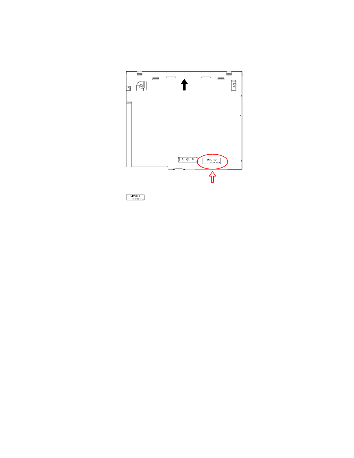
2.1 Identification method
Supported reduction in cost, and board contents and mechanism contents were changed.
A set put the following label on is an object.
Top view
Front side
Label position
Change pwb and mechanism parts
1-10 (No.MA437<Rev.003>)
SECTION 3
DISASSEMBLY
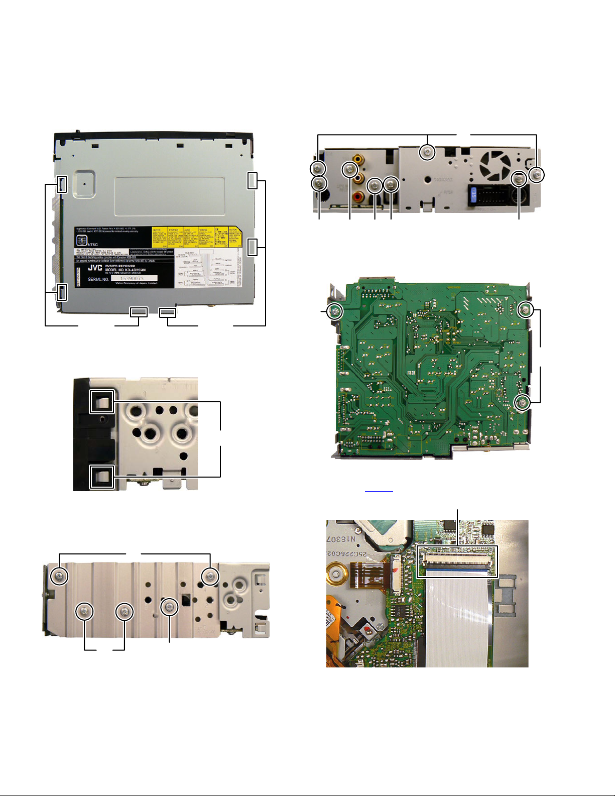
3.1 Main body (Used figure are KD-ADV5580J)
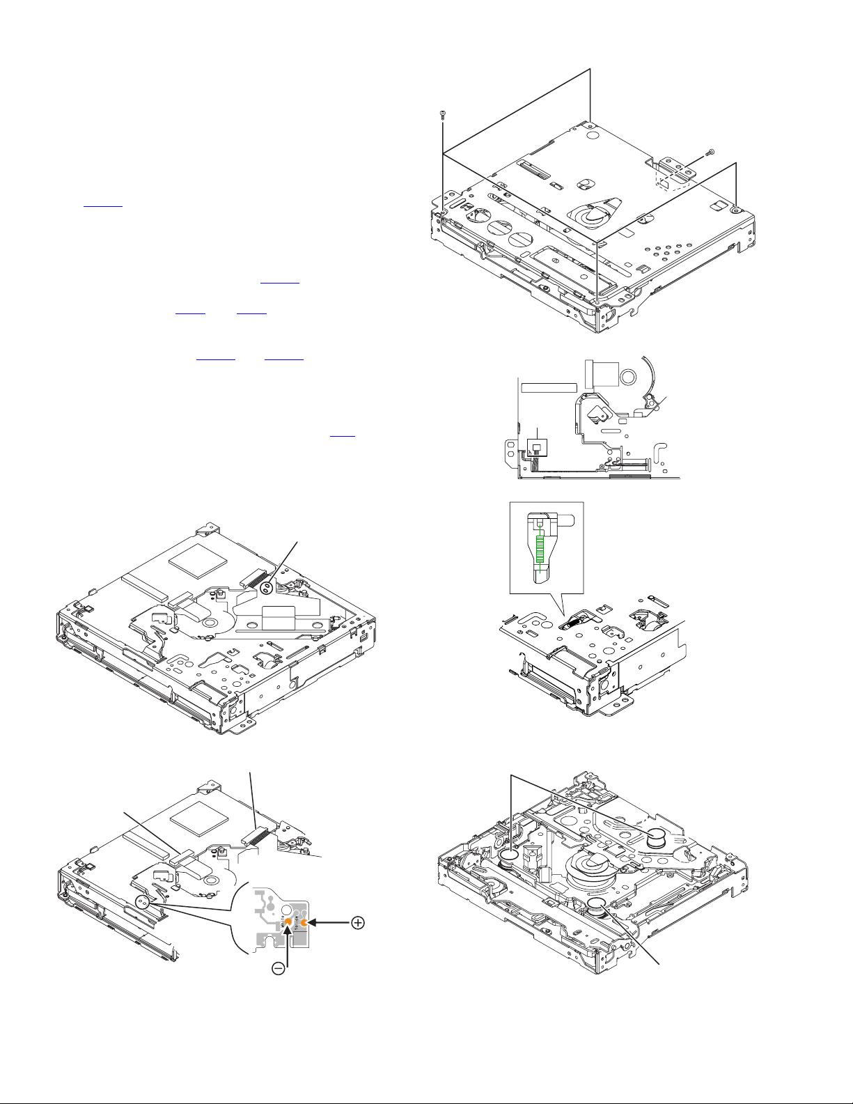
3.1.1 Removing the Bottom chassis (See Fig.1)
(1) Disengage six hooks a engaged Bottom chassis.
Fig.1
3.1.2 Removing the Front chassis (See Fig.2)
(1) Disengage four hooks b both side of the Front chassis.
Fig.2
3.1.3 Removing the Heat sink (See Fig.3)
(1) Remove the two screws A, two screws B and one screw C
attaching the Heat sink.
Fig.3
3.1.4 Removing the Main board (See Fig.4 to 6)
(1) Remove the three screws D, two screws E, two screws F
and one screw G attaching the Rear bracket. (See Fig.4)
Fig.4
(2) Remove the three screws H attaching the Main board. (See
Fig.5)
Fig.5
(3) Disconnect the card wire from Main board connected to
connector CN403
of the Front end board. (See Fig.6)
Fig.6
REFERENCE: Screw E, F and G are attaching and can take
off the main board.
hook
a
hook
a
hook
b
BC
A
EFGF E
D
H
H
CN403
(No.MA437<Rev.003>)1-11
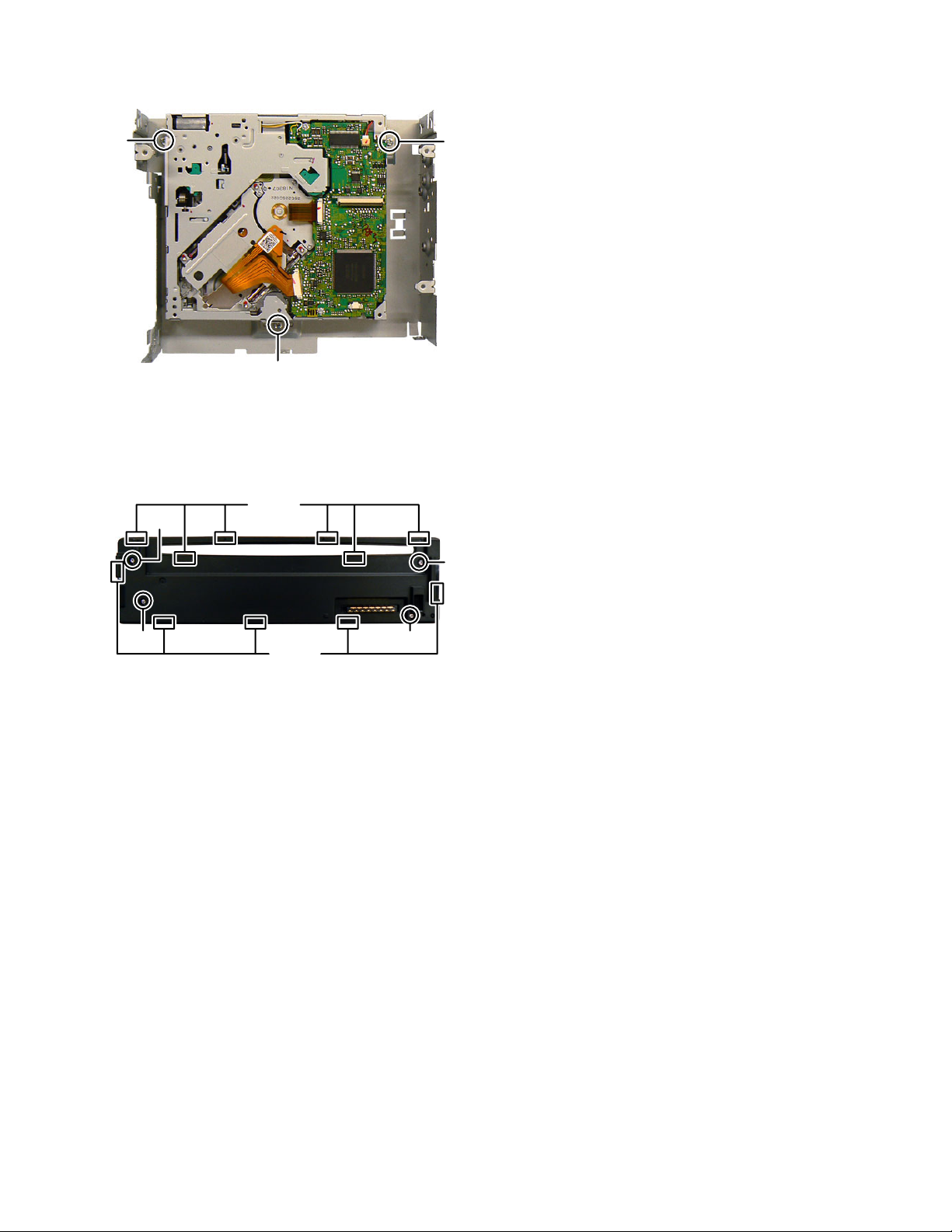
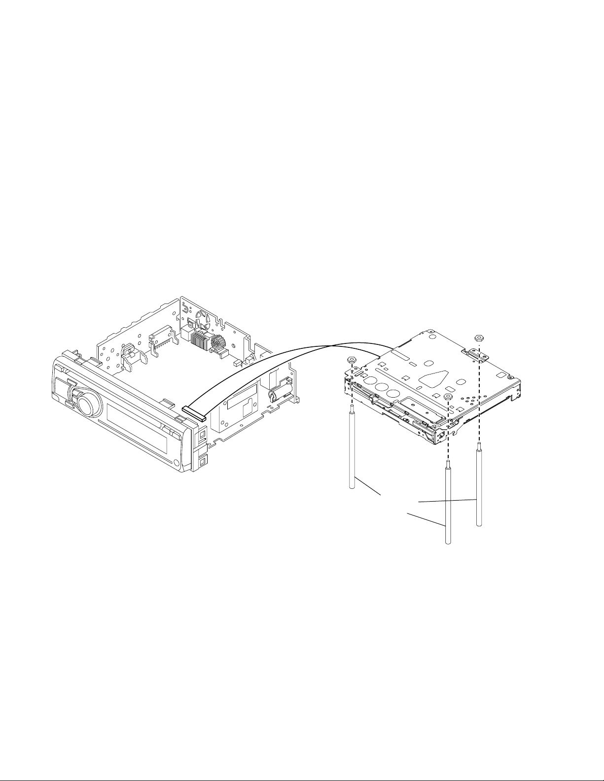
3.1.5 Removing the DVD mechanism (See Fig.7)
(1) Remove the three screws J attachin g the DVD mechan ism.
Fig.7
3.1.6 Removing the Switch board (See Fig.8)
(1) Remove the Volume knob.
(2) Remove the four screws K attaching the Rear cover .
(3) Disengage eleven hooks c engaged Rear cover.
Fig.8
J
JJ
K
KK
K
hook
c
hook
c
1-12 (No.MA437<Rev.003>)
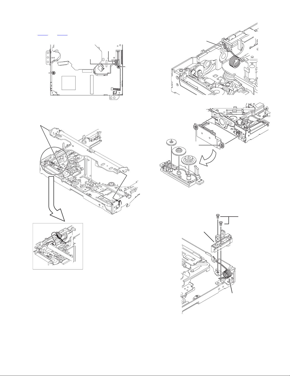
3.2 DVD mechanism assembly section
3.2.1 Removing the Traverse mechanism assembly (See
Fig.1 to 6)
(1) Solder the short land section on the flex ib le wire of pickup.
(See Fig.1)
Caution:
* Solder the short land section on the flexible wire of pickup
before disconnecting the flexible wir e form the connector
CN101
on the Front end board.
If the flexible wire is disconnected without attaching the
solder, the pickup may be destroyed by static electricity.
* When attaching the Tr averse mechanism assembly, re-
move the solder from the short land section after connection
the flexible w ire to the connector CN101
on the Front end
board.
(2) Voltage supply to TP79
and TP81 approx DC 3.0V until
Clamper is shift to loading complete position. (See Fig.2)
(3) Disconnect the flexible wires from Traverse mechanism assembly
connected to connector CN101
and CN164 of the Front end
board. (See Fig.2)
(4) Remove the five screws A attaching the Top cover assembly.
(See Fig.3)
(5) From the bottom side, disconnect the connector wire from
Top cover assembly connected to connector CN2
of the
Front end board. (See Fig.4)
(6) From the bottom side, remove the spring from Traverse
mechanism assembly. (See Fig.5)
(7) From the top side, pull up the traverse mechanism and disenga ge
three dumper positions. (See Fig.6)
Fig.1
Fig.2
Fig.3
Fig.4
Fig.5
Fig.6
Solder short part
CENTER
R21
D-
DGND_7
R312
R317
WOOFER
TP67
R357
TP79 TP81
TP92
Voltage supply
position
CN164
CN101
TP81
TP79
A
CN2
Dumper
(same color spring)
Dumper
(Different color spring)
(No.MA437<Rev.003>)1-13
3.2.2 Removing the Front end board (See Fig.7)
(1) Remove the Motor wires from loading motor soldered to
TP79
and TP81 of the Front end board.
(2) Remove the two screws B attaching the Front end board.
Fig.7
3.2.3 Removing the Loading arm assembly (See Fig.8)
(1) Remove the Loading arm spring L from Loading arm assembly.
(2) Slide to left side and then disengage hook a then hook b.
Fig.8
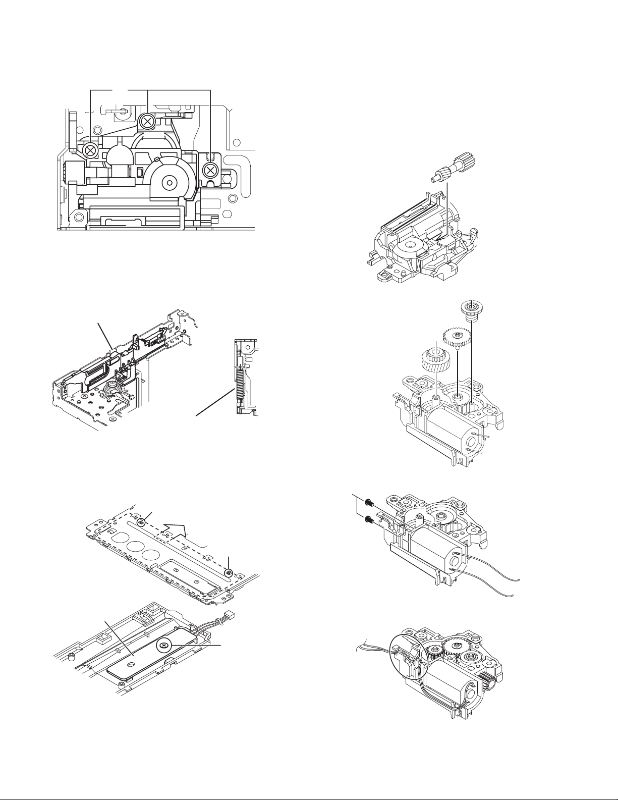
3.2.4 Removing the Gear base assembly (See Fig.9, 10)
(1) Remove the Loading arm spring L. (See Fig.9)
(2) Remove the two screws C attaching the Gear base assembly.
(See Fig.10)
Fig.9
Fig.10
3.2.5 Removing the Loading arm holder. (See Fig.11)
(1) Remove the two screws D attaching the Loading arm holder.
(2) Remove the Loading arm spring R.
Fig.11
B
B
TP79
TP81
Loading arm
assembly
Loading arm spring L
hook
a
hook b
Loading arm
spring L
C
D
Loading arm
spring R
Loading arm
holder
1-14 (No.MA437<Rev.003>)
3.2.6 Removing the Loading moor assembly (See Fig.12)
(1) Remove the three screws E attaching the Loading motor
assembly.
Fig.12
3.2.7 Removing the Slide cam assembly (See Fig.13)
(1) Slide to backward the Slide c am as semb ly an d the r em ove
the Slide cam spring.
(2) Slide to frontward the slide cam assembly, and then take
out it.
Fig.13
3.2.8 Removing the Photo board (See Fig.14)
(1) Pressing the hook c and then slide to backward (sl ide to the
arrow side) the Disc plate.
(2) Remove the one screw F attaching the Photo board.
Fig.14
3.2.9 Removing the Loading motor (See Fig.15 to 18)
(1) Remove the A wheel gear. (See Fig.15)
(2) Remove the A worm gear, M connect gear and M wheel
gear by sequentially. (See Fig.16)
(3) Remove the two screws G attaching the Loading motor.
(Se Fig.17)
(4) When attaching the Loading motor, motor wire should arrange
to figure. (See Fig .18)
Fig.15
Fig.16
Fig.17
Fig.18
E
Slide cam assembly
Slide cam spring
hook
c
hook
c
F
Photo board
A Wheel gea
r
A worm gear
M connect gear
M wheel gear
G
Wire arrangement
(No.MA437<Rev.003>)1-15
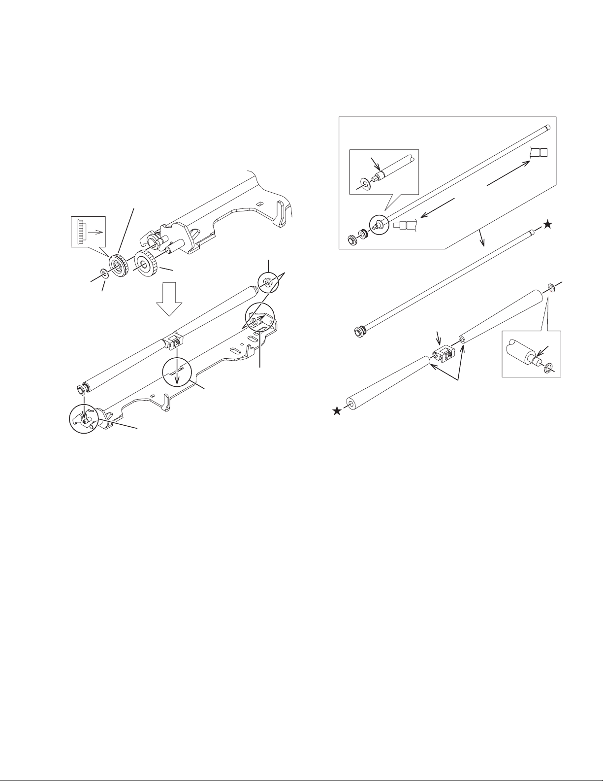
3.2.10 Removing the Roller assembly (See Fig.19)
(1) Remove the Slit washer.
(2) Remove the R middle gear.
(3) Remove the R connect gear.
(4) Snap off the part a of the Roller assembly.
(5) Lift up the part b of the Roller assembly, and then release
part c (When release part c, R co llar R is eas y to come off,
does not lose it).
CAUTION:
When reattach the Roller assembly, Middle gear should keep
direction and Slit washer should be change new part.
Fig.19
3.2.11 Removing the Roller (See Fig.20)
(1) Remove the Slit washer.
(2) Pull out the Roller shaft.
CAUTION:
When reattach the Roller shaft, Slit washer should be change
new part.
Fig.20
Direction
Slit washer
R connect gear
R collar R
R middle gear
part b
part a
part c
keep direction
slit
small side
keep direction
slit
1-16 (No.MA437<Rev.003>)
SECTION 4
ADJUSTMENT
4.1 Test instruments required for adjustment
(1) Digital oscilloscope (100MHz)
(2) Jitter meter
(3) Digital tester
(4) Electric voltmeter
(5) Tracking offset meter
(6) Test Disc : VT501 or VT502
(7) Extension studs : STDV001-3P
(8) Extension cable : EXTAV70X-50PF
4.2 Standard measuring conditions
Power supply voltage DC14.4V(11V to 16V)
Load impedance 4 Ω(2 Speakers connection)
Line output 20kΩ
Caution:
Be sure to attach the heat sink and rear bracket onto th e power
amplifier IC and regulator IC respectively, before supply the
power.
If voltage is applied without attaching these parts, the power
amplifier IC and regulator IC will be destroyed by heat.
4.3 Connection method
Connection procedure
Attach the front chassis assembly to the main board.
Connect the front panel assembly to the main board.
Attach the heat sink and rear bracket to the main board.
Attach the extension studs to the DVD mechanism assembly.
Connect the DVD mechanism assembly and the main board with a extension cable.
STDV001-3P
EXTAV70X-50PF
(No.MA437<Rev.003>)1-17
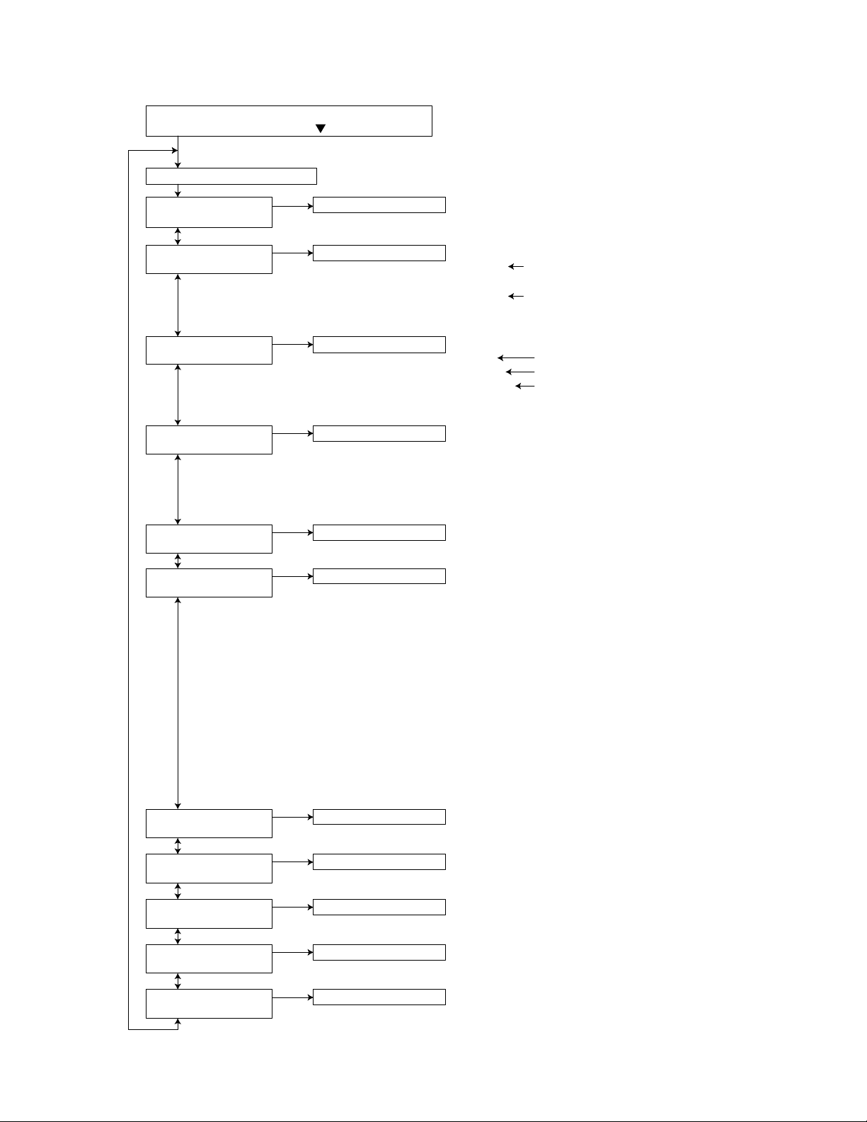
4.4 Service mode
Power ON.
Keep this state more than 3 seconds while continuing
pressing the [MENU] button and [ ] button sequentially.
Exchanging it operate a menu of service mode with the [FF] button and [REW] button.
Operate choice of a menu with a [ENT] button.
The unit enters the service mode.
"INIT" is
indicated on the LCD.
Press the [ENT] button Initialize user set data
: The system control EEPROM is initialized except
for The loading/ejection error history.
"VERSION" is
indicated on the LCD.
Press the [ENT] button Micon version display
S-XXX-YY
System control CPU version/
ROM correction version
DVD-XXX
*Exchanging it operate each indication with the
[FF] button and [REW] button.
DVD version
"AREA/RGN" is
indicated on the LCD.
Press the [ENT] button Destination area/region display
SYS-XX
DVD-AXX
DVDRGN X
*Exchanging it operate each indication with the
[FF] button and [REW] button.
System control destination
DVD unit destination
DVD unit region
"VIDEO" is
indicated on the LCD.
Press the [ENT] button Setting of NTSC or PAL
"NTSC" or "PAL" are indicated on the LCD.
*Exchanging it operate each indication with the
[FF] button and [REW] button.
Note:
There is the model that is not equipped with
this mode by a version.
"CLR ERR" is
indicated on the LCD.
Press the [ENT] button Clear loading/ejection error history
:The error history stored in the EEPROM is cleared.
"CD ERROR" is
indicated on the LCD.
Press the [ENT] button Read loading and ejection error history
:The error history saved in the system control
is read and displayed.
"DVD-TEMP" is
indicated on the LCD.
Press the [ENT] button Thermistor's temperature data readout
: Data in the temperature sensor in the DVD unit
is read every 5 seconds and displayed in hex numbers.
"SYS-TEMP" is
indicated on the LCD.
Press the [ENT] button Thermistor's temperature data readout
: Data in the temperature sensor in the system control
is read every 5 seconds and displayed in hex numbers.
"CHK MODE" is
indicated on the LCD.
Press the [ENT] button DVD unit check mode
(See section "DVD check mode" for details.)
"RUNNING" is
indicated on the LCD.
Press the [ENT] button Running mode : For use in running tests.
"MEMCHECK" is
indicated on the LCD.
Press the [ENT] button Memory check
: The remaining data capacity of the disc is displayed on the LCD.
TOT-XXXX : Total error count.
(A figure between 0 and 9999 is displayed.
10000 or more is also displayed as 9999.)
Enyyzzzz : Latest three error history
n: Counter
yy: Error code
zzzz: Detailed error code
0nyyzzz : First five error history
n: Counter
yy: Error code
zzzz: Detailed error code
*Exchanging it operate each indication with the
[FF] button and [REW] button.
(See section "Error code tables" for details.)
1-18 (No.MA437<Rev.003>)
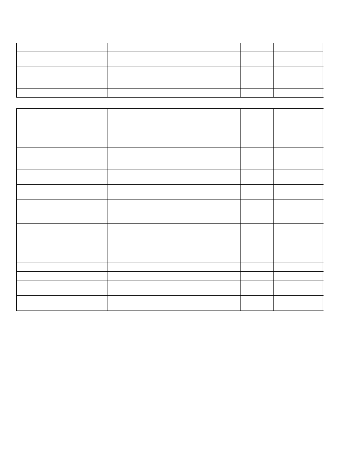
4.5 Error code tables
4.5.1 Mechanism error code
4.5.2 Disc error code
Error contents Details Error code Detailed error code
Disc loading error
(1)D1 time out 09 0013
Eject error
(1)B1 time out
(2)C1 time out
01
01
0023
0024
Error in loading wait Loading of a running mo de Disc was pulled out in a w ait. 09 0031
Error contents Details Error code Detailed error code
TOC read error TOC read movement of a CD is not completed. 84 0059
First track access error Even if TOC reading passes after the end with CD run-
ning mode for 30 s econds, the first track access is not fin-
ished.
80 0060
Last track access error Even if first track passes after the end with CD running
mode for 30 seconds, the last track access is not fin-
ished.
80 0061
T1 access error Eve n if T1 access passes in a DVD running mode for 30
seconds, it is not finished.
80 0069
T12 access error Even if T12 ac cess passes in a DVD ru nning mode for 30
seconds, it is not finished.
80 0070
T24 access error Even if T24 access passes in a DVD running mode for
30 seconds, it is not finished.
80 0071
Read-in area read error Read-in area read operation of DVD is not completed. 84 0072
DVD L1 layer adjustment error Adjustment of L1 layer of DVD is not finished normally.
(including focus jump failure)
80 0074
DVD L0 layer adjustment error Adjustment of L0 layer of DVD is not finished normally.
(including focus jump failure)
80 0075
NO DISC judgment Judgment without disc. 80 0090
It is NO DISC by start failure Start is impossible 80 0091
It is stopped by playback inability Stop in running mode playback 80 0093
Logic format NG Logic format analysis inability or non-correspondence
logic format
80 0094
Seek access error It cannot arrive a t an ai m add ress eve n if i t pass es fo r 15
seconds.
80 0095

(No.MA437<Rev.003>)1-19
4.6 DVD check mode
Change LCD indication with a [FF] button and a [REW] button.
Operate choice of a menu with a [ENT] button.
LCD indication DVD unit operation
Example of LCD
indication
Indication contents
TEST-1 Start at normal speed
(After start, it is measured JITTER on the internal position)
NORMPLAY
CUR ****
JIT ****
Laser current value
Jitter value
TEST-2 Tracking off on The outermost position of CD EF-BAL
OUTROFF For EF phase error
TEST-3 Tracking off on The innermost position of CD EF-BAL
INNTROFF For EF phase error
TEST-4 CD_LD lights and laser current is displayed CDLD ON
CUR ****
JIT ****
Laser current value
Jitter value
TEST-5 DVD_LD lights and laser current is displayed DVDLD ON
CUR ****
JIT ****
Laser current value
Jitter value
TEST-6 DVD ×1 jitter measuring mode
(for use in mechanism measurement)
DVD×1JIT
CUR ****
JIT ****
Laser current value
Jitter value
TEST-7 Indication of EEPROM contents ROM DATA
ADDR ****
DATA ****
EEPROM address
EEPROM contents
TEST-8 Indication of EEPROM contents ROM DATA
ADDR ****
DATA ****
EEPROM address
EEPROM contents
TEST-9 Initialization of EEPROM contents ROMCLEAR
TEST-10 Indicati on of temperature TEMP
TEMP **** Temperature
TEST-11 Search & jitter measurement to an appointed position of DVD DVD JIT
PLC ****
JIT ****
(Position measured with
VT-501 jitter value)
TEST-12 Setting of MONITOR terminal MONITOR
M1 ****
M2 ****
TEST-13 DVD ×1 double speed start
(After start, it is measured JITTER on the internal position)
×1PLAY
CUR ****
JIT ****
Laser current value
Jitter value
[DISC DW ] Disc stopped & LD-OFF STOP
[EJECT] EJECT OPEN

1-20 (No.MA437<Rev.003>)
SECTION 5
TROUBLESHOOTING
5.1 16 PIN CORD DIAGRAM (for KD-ADV5580, KD-DV5500)
8
7
6
5
16
15
13
4
3
2
1
12
11
10
9
BK
RD
WH
GN
VI
GY
BL/WH
GN/BK
VI/BK
GY/BK
YL
NC
WH/BK
NC
14
NC
YG
YL
BK
GN/BK
VI/BK
VI
WH
WH/BK
9
1
3
16
11
10
5
6
GY/BK
12
YG
14
BL/WH
GY
GN
7
2
8
RD
Black
RD
BK
Red
BL
Blue
WH
White
GN
Green
GY
Gray
Yellow
VI
Violet
YL
Yellow Green
YG
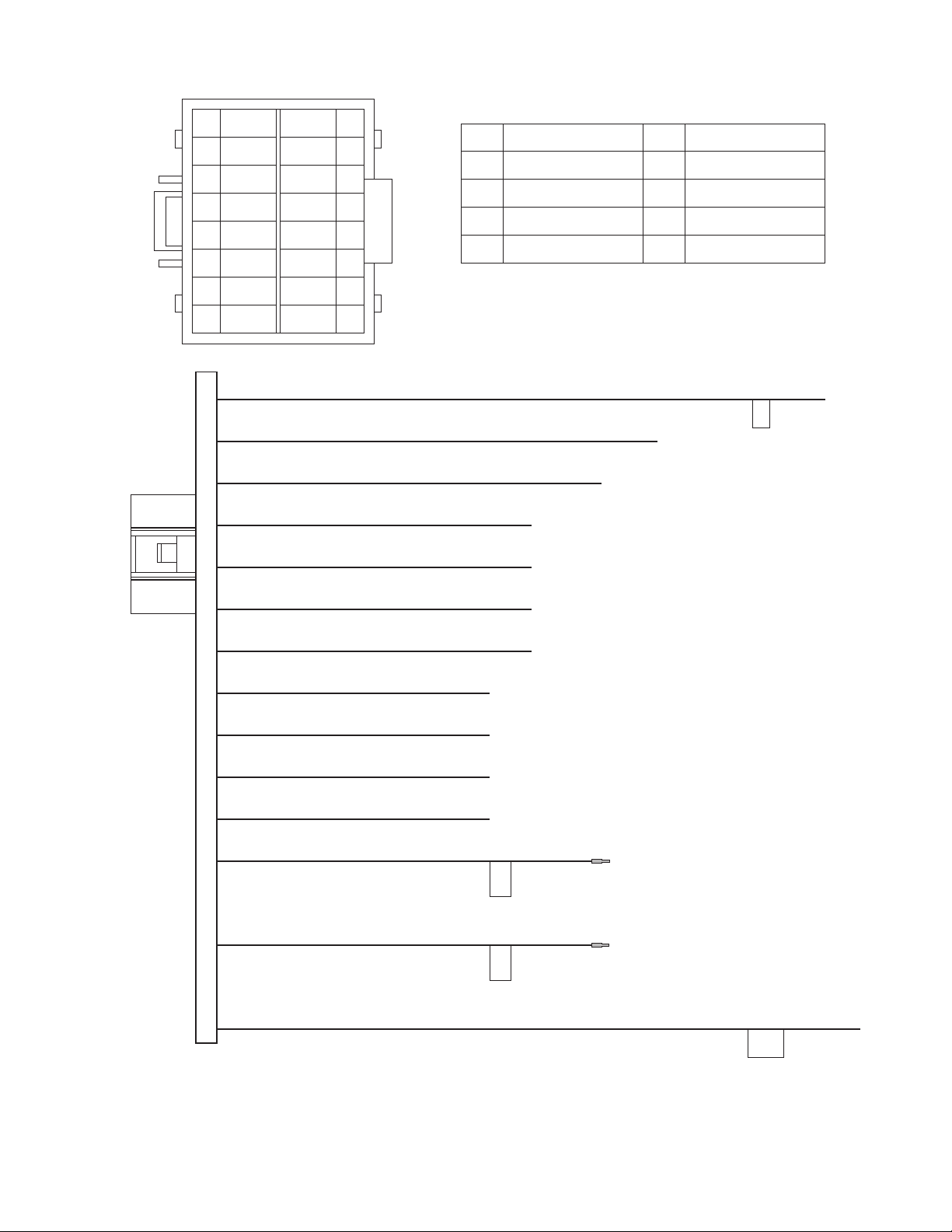
(No.MA437<Rev.003>)1-21
5.2 16 PIN CORD DIAGRAM (for KD-DV4504, KD-DV4505, KD-DV4506, KD-DV4588)
Black
RD
BK
Red
BL
Blue
WH
White
GN
Green
GY
Gray
Yellow
VI
Violet
YL
Yellow Green
YG
8
7
6
5
16
15
13
4
3
2
1
12
11
10
9
BK
RD
WHGN
VI
GY
BL/WH
GN/BK
VI/BK
GY/BK
YL
BL
WH/BK
NC
14
NC
YG
YL
BK
GN/BK
VI/BK
VI
WH
WH/BK
9
1
3
16
11
10
5
6
GY/BK
12
YG
14
BL/WH
GY
GN
7
2
8
RD
4
BL

(No.MA437<Rev.003>)
VSE
Printed in Japan
Victor Company of Japan, Limited
Mobile Entertainment Division 10-1,1chome,Ohwatari-machi,Maebashi-city,371-8543,Japan
REVISION INFORMATION
DVD/CD RECEIVER
COPYRIGHT © 2009 Victor Company of Japan, Limited
MA437-R002
2009/08
KD-ADV5580J, KD-DV5500J, KD-DV4504UI,
KD-DV4505U, KD-DV4505UN, KD-DV4505UT,
KD-DV4505A, KD-DV4506U, KD-DV4506UN,
KD-DV4506UT, KD-DV4506A, KD-DV4588UF,
KD-DV4505UH, KD-DV4506UH
■ OVERVIEW
Add KD-DV4505UH and KD-DV4506UH.
■ DETAILS
COVER SECTION
Title Line No.MA437<Rev.001> No.MA437<Rev.002> Description
Revision Rev.001 Rev.002
Issue Date 2009/01 2009/08
Model No. KD-ADV5580J, KD-DV4504UI, KD-DV4505A,
KD-DV4505U, KD-DV4505UN, KD-DV4505UT,
KD-DV4506A, KD-DV4506U, KD-DV4506UN,
KD-DV4506UT, KD-DV4588UF, KD-DV5500J
KD-ADV5580J, KD-DV4504UI, KD-DV4505A,
KD-DV4505U, KD-DV4505UH, KD-DV4505UN,
KD-DV4505UT, KD-DV4506A, KD-DV4506U,
KD-DV4506UH, KD-DV4506UN, KD-DV4506UT,
KD-DV4588UF, KD-DV5500J
SECTION 2 SPECIFIC SERVICE INSTRUCTIONS
Title Line No.MA437<Rev.001> No.MA437<Rev.002> Description
2 SPECIFIC SERVICE
INSTRUCTIONS
1 This servi ce manual does not describe
SPECIFIC SERVIC E INSTRUCTIONS.
-
2.1 Identification method T - 2.1 Identification method
1 - Supported reduction in cost, and board
contents was changed.A set put the following
label on is an object.
2 - ILLUSTRATION(ma437_2001.png)
2 (MA437-R002)
STANDARD SCHEMATIC DIAGRAMS
Schematic Diagram
Diagram Name No.MA437<Rev.001> No.MA437<Rev.002> Description
Menu Main section Old Main section (Except DV4505/4506UH)
Menu - Main section (Common)
ma437_s005.svgz
Printed Circuit Board
Diagram Name No.MA437<Rev.001> No.MA437<Rev.002> Description
Menu Main Board Old Main Board (Except DV4505/4506UH)
Menu - Main Board (Common)
ma437_p005.svgz
Description of Major ICs
Diagram Name No.MA437<Rev.001> No.MA437<Rev.002> Description
Menu IC1: TEF6606T/V3-X IC1: TEF6606T/V5-X
PARTS LIST
MODEL No. LIST
Model No. No.MA437<Rev.002>
KD-ADV5580J 01
KD-DV4504UI 03
KD-DV4505A 07
KD-DV4505U 04
KD-DV4505UH 0D
Model No. No.MA437<Rev.002>
KD-DV4505UN 05
KD-DV4505UT 06
KD-DV4506A 0B
KD-DV4506U 08
KD-DV4506UH 0E
Model No. No.MA437<Rev.002>
KD-DV4506UN 09
KD-DV4506UT 0A
KD-DV4588UF 0C
KD-DV5500J 02
General assembly [M1MM]
Part No.
!
Symbol o
r
<Rev.001> <Rev.002>
Part Name Description Qty Models
M1MM 11 ------------ GE10242-005A FRONT
CHASSIS
(Addition) 1 0D,0E
M1MM 38 ------------ GE32926-002A INSULATOR (Addition) 1 0D,0E
M1MM 56 ------------ LV45386-001A R2
INDICATION
(Addition) 1 01,02,03,04,05,06,07,08,09,0A,0B,0C,0D,0E
Switch board [02]
Part No.
!
Symbol or
<Rev.001> <Rev.002>
Part Name Description Qty Models
02 R654 ------------ NRSA63J-511X MG RESISTOR (Addition) 1 0D,0E
Main board common [04]
Part No.
!
Symbol or
<Rev.001> <Rev.002>
Part Name Description Qty Models
! 04 IC1 ------------ TEF6606T/V5-X IC (Addition) 1 01,02,03,04,05,06,07,08,09,0A,0B,0C,
0D,0E
04 IC161 ------------ BD3700FV-X IC (Addition) 1 01,02,03,04,05,06,07,08,09,0A,0B,0C,
0D,0E
! 04 IC301 ------------ TB2926CHQ IC (Addition) 1 01,02,03,04,05,06,07,08,09,0A,0B,0C,
0D,0E
04 IC361 ------------ NJM2160BV-X IC (Addition) 1 01
04 IC402 ------------ TOTX177L OPT
TRANSMITTER
(Addition) 1 01,02,03,04,05,06,07,08,09,0A,0B,0C,
0D,0E
04 IC411 ------------ MM1510XN-X IC (Addition) 1 01,02,03,04,05,06,07,08,09,0A,0B,0C,
0D,0E
04 IC471 ------------ NJM4565E-X IC (Addition) 1 01,02,03,04,05,06,07,08,09,0A,0B,0C,
0D,0E
! 04 IC721 ------------ JES1552 IC (Addition) 1 01,02,03,04,05,06,07,08,09,0A,0B,0C,
0D,0E
04 IC801 ------------ SN74AHCT126PW-X IC(DIGITAL) (Addition) 1 01,02,03,04,05,06,07,08,09,0A,0B,0C,
0D,0E
! 04 IC911 ------------ R2S25400DS-E IC (Addition) 1 01,02,03,04,05,06,07,08,09,0A,0B,0C,
0D,0E

(MA437-R002) 3
Part No.
!
Symbol or
<Rev.001> <Rev.002>
Part Name Description Qty Models
! 04 IC922 ------------ LV5749V-X IC (Addition) 1 01,02,03,04,05,06,07,08,09,0A,0B,0C,
0D,0E
04 IC952 ------------ NJM2878F4-33-X IC (Addition) 1 01,02,03,04,05,06,07,08,09,0A,0B,0C,
0D,0E
04 Q301 ------------ 2SC1623A/5-6/-X TRANSISTOR (Addition) 1 01,02,03,04,05,06,07,08,09,0A,0B,0C,
0D,0E
04 Q301 or ------------ 2SC3928A/QR/-X TRANSISTOR (Addition) 1 01,02,03,04,05,06,07,08,09,0A,0B,0C,
0D,0E
04 Q321 ------------ IMX9-W PAIR
TRANSISTOR
(Addition) 1 01,02,03,04,05,06,07,08,09,0A,0B,0C,
0D,0E
04 Q701 ------------ RT1N141C-X DIGI
TRANSISTOR
(Addition) 1 01,02,03,04,05,06,07,08,09,0A,0B,0C,
0D,0E
04 Q701 or ------------ UN2211-X TRANSISTOR (Addition) 1 01,02,03,04,05,06,07,08,09,0A,0B,0C,
0D,0E
04 Q702 ------------ RT1P141C-X DIGI
TRANSISTOR
(Addition) 1 01,02,03,04,05,06,07,08,09,0A,0B,0C,
0D,0E
04 Q702 or ------------ UN2111-X TRANSISTOR (Addition) 1 01,02,03,04,05,06,07,08,09,0A,0B,0C,
0D,0E
04 Q703 ------------ RT1N141C-X DIGI
TRANSISTOR
(Addition) 1 01,02,03,04,05,06,07,08,09,0A,0B,0C,
0D,0E
04 Q703 or ------------ UN2211-X TRANSISTOR (Addition) 1 01,02,03,04,05,06,07,08,09,0A,0B,0C,
0D,0E
04 Q704 ------------ RT1P141C-X DIGI
TRANSISTOR
(Addition) 1 01,02,03,04,05,06,07,08,09,0A,0B,0C,
0D,0E
04 Q704 or ------------ UN2111-X TRANSISTOR (Addition) 1 01,02,03,04,05,06,07,08,09,0A,0B,0C,
0D,0E
04 Q851 ------------ 2SB1132/QR/-W TRANSISTOR (Addition) 1 03,04,05,06,07,08,09,0A,0B,0C,0D,0E
04 Q852 ------------ RT1N141C-X DIGI
TRANSISTOR
(Addition) 1 03,04,05,06,07,08,09,0A,0B,0C,0D,0E
04 Q852 or ------------ UN2211-X TRANSISTOR (Addition) 1 03,04,05,06,07,08,09,0A,0B,0C,0D,0E
04 Q861 ------------ RT1P141C-X DIGI
TRANSISTOR
(Addition) 1 01,02,03,04,05,06,07,08,09,0A,0B,0C,
0D,0E
04 Q861 or ------------ UN2111-X TRANSISTOR (Addition) 1 01,02,03,04,05,06,07,08,09,0A,0B,0C,
0D,0E
04 Q862 ------------ RT1P141C-X DIGI
TRANSISTOR
(Addition) 1 01,02,03,04,05,06,07,08,09,0A,0B,0C,
0D,0E
04 Q862 or ------------ UN2111-X TRANSISTOR (Addition) 1 01,02,03,04,05,06,07,08,09,0A,0B,0C,
0D,0E
04 Q885 ------------ RT1N141C-X DIGI
TRANSISTOR
(Addition) 1 01,02,03,04,05,06,07,08,09,0A,0B,0C,
0D,0E
04 Q885 or ------------ UN2211-X TRANSISTOR (Addition) 1 01,02,03,04,05,06,07,08,09,0A,0B,0C,
0D,0E
! 04 Q921 ------------ MCH6406-W MOS
TRANSISTOR
(Addition) 1 01,02,03,04,05,06,07,08,09,0A,0B,0C,
0D,0E
! 04 Q922 ------------ MCH6406-W MOS
TRANSISTOR
(Addition) 1 01,02,03,04,05,06,07,08,09,0A,0B,0C,
0D,0E
04 Q951 ------------ RT1P441C-X DIGI
TRANSISTOR
(Addition) 1 01,02,03,04,05,06,07,08,09,0A,0B,0C,
0D,0E
04 Q951 or ------------ UN2113-X TRANSISTOR (Addition) 1 01,02,03,04,05,06,07,08,09,0A,0B,0C,
0D,0E
04 Q952 ------------ RT1N441C-X TRANSISTOR (Addition) 1 01,02,03,04,05,06,07,08,09,0A,0B,0C,
0D,0E
04 Q952 or ------------ UN2213-X DIGI
TRANSISTOR
(Addition) 1 01,02,03,04,05,06,07,08,09,0A,0B,0C,
0D,0E
04 Q976 ------------ RT1N441C-X TRANSISTOR (Addition) 1 01,02,03,04,05,06,07,08,09,0A,0B,0C,
0D,0E
04 Q976 or ------------ UN2213-X DIGI
TRANSISTOR
(Addition) 1 01,02,03,04,05,06,07,08,09,0A,0B,0C,
0D,0E
04 Q977 ------------ 2SA812A/5-6/-X TRANSISTOR (Addition) 1 01,02,03,04,05,06,07,08,09,0A,0B,0C,
0D,0E
04 Q977 or ------------ ISA1530AC1/QR/X TRANSISTOR (Addition) 1 01,02,03,04,05,06,07,08,09,0A,0B,0C,
0D,0E
04 D302 ------------ 1SS355W-X DIODE (Addition) 1 01,02,03,04,05,06,07,08,09,0A,0B,0C,
0D,0E
04 D302 or ------------ MA111-X SI DIODE (Addition) 1 01,02,03,04,05,06,07,08,09,0A,0B,0C,
0D,0E
04 D322 ------------ MC2836-X DIODE (Addition) 1 01,02,03,04,05,06,07,08,09,0A,0B,0C,
0D,0E
04 D322 or ------------ MA152WA-X DIODE (Addition) 1 01,02,03,04,05,06,07,08,09,0A,0B,0C,
0D,0E
Loading...