


 Loading...
Fiber Optic “Light to Logic”
Receiver
Preliminary Technical Data
RCV1551
Features
•Light to Logic 20-pin DIP Receiver Offers ECL Compatibility
•Long Reach, High Performance
•Sensitivity -35 dBm
•Single +5 V Supply
•SONET/SDH Compliant
•Multisourced
Applications
•Telecommunication Networks
•SONET OC3 and SDH STM1 Compatible
•Local and Metropolitan Area Networks
•ATM Single Mode Public Network
•Military Communications and Control Systems Performance
•Digital Cable TV Networks
Description
The RCV1551 receiver provides optical signal conversion and processing. It contains an InGaAs PIN photodiode and high sensitivity, wide dynamic range, transimpedance amplifier, capacitively coupled to limiting amplifier stages with PECL output drivers. Also provided is a loss of signal alarm.
The planar PIN photodiode operates throughout the 1200 nm to 1600 nm wavelength band. A CMOS wide dynamic range transimpedance amplifier optimized for 155 MBd operation provides low noise front end gain for the RCV1551.
A low pass filter maximizes the signal to noise ratio while minimizing intersymbol interference. The interface amplifier provides signal conversion and buffering for the PECL complementary data outputs. A complementary PECL alarm output is also provided.
The receiver operates from +5 V and -5.2 V or +5 V and Ground power supplies. A 50/125 micron multimode fiber pigtail is included, assuring compatibility with multimode and single mode fiber optic systems.
Preliminary Product Disclaimer
This preliminary data sheet is provided to assist you in the evaluation of engineering samples of the product which is under development and targeted for release during 1997. Until Hewlett-Packard releases this product for general sales, HP reserves the right to alter prices, specifications, features, capabilities, function, manufacturing release dates, and even general availability of the product at any time.
418 |
(5/97) |
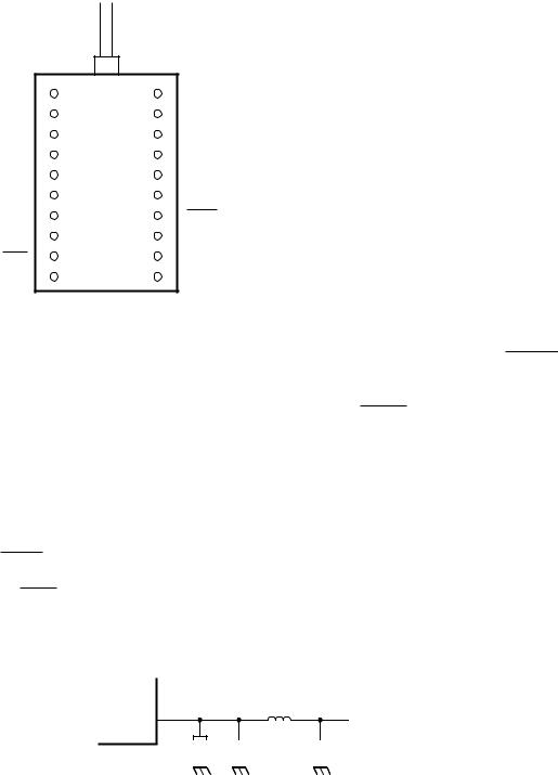
Connection Diagram
Top View
|
|
FIBER PIGTAIL |
|
GND |
1 |
20 |
NC |
GND |
2 |
19 |
NC |
GND |
3 |
18 |
NC |
GND |
4 |
17 |
NC |
NC |
5 |
16 |
GND |
GND |
6 |
15 |
GND |
DATA |
7 |
14 |
ALARM |
GND |
8 |
13 |
GND |
DATA |
9 |
12 |
ALARM |
PD BIAS |
10 |
11 |
+5 V |
Pin Descriptions
Pins 5, 17, 18, 19, 20 NC:
These pins are not connected and should be left open circuit on the application PCB.
Pins 1, 2, 3, 4, 6, 8, 13, 15, 16
GND:
These pins should be connected to the circuit ground.
Pins 7, 9, DATA, DATA:
These pins provide complementary PECL DATA and DATA outputs. The DATA output is noninverting, an optical pulse causes the DATA output to go to the PECL logic high state (+4 V nominal).
Pin 10, PD Bias:
This pin must be connected to any voltage from 0 V (GND) to -5 V. This provides the photodiode bias. The current drawn is directly proportional to the average received photocurrent.
I = Responsitivity x Mean Power.
The responsivity will be between 0.7 A/W and 1.0 A/W.
Pin 11, +5 V:
This pin should be connected to +5 V supply. The network shown below should be placed as close as possible to pin 11.
Pins 12, 14 ALARM, ALARM:
These pins provide complementary differential ALARM and ALARM outputs. This is the low light alarm. ALARM goes to a logic low (3.3 V nominal) state when the optical power drops below the threshold level (insufficient optical power).
The optical power must increase to a higher level than the level where the alarm went low before ALARM will return to a logic high. This difference is the alarm hysteresis.
1 µH
 +5 V
+5 V
PIN 11
10 µF |
|
|
|
|
|
100 nF |
|
|
100 nF |
|
|
|
|
|
|
|
|
|
|
419
Loading...