


www.fairchildsemi.com
FEB388_003
FAN9611/FAN9612 400W Interleaved
Dual BCM PFC Controller
Evaluation Board User Guide
Featured Fairchild Product: FAN9611, FAN9612
Please contact a local Fairchild Sales representative for an evaluation board.
© 2010 Fairchild Semiconductor Corporation |
1 |
FEB388_FAN9611/12 • Rev. 0.0.3 |

www.fairchildsemi.com
Table of Contents
1. |
Overview of the Evaluation Board ........................................................................................... |
3 |
|
2. |
Key Features ............................................................................................................................. |
4 |
|
3. |
Specifications............................................................................................................................ |
5 |
|
4. |
Test Procedure .......................................................................................................................... |
6 |
|
5. |
Schematic.................................................................................................................................. |
7 |
|
6. |
Boost Inductor Specification .................................................................................................... |
8 |
|
7. |
Line Filter Inductor Specifications ........................................................................................... |
9 |
|
8. |
PCB Layout............................................................................................................................. |
10 |
|
9. |
Bill of Materials (BOM) ......................................................................................................... |
14 |
|
10. |
Test Results............................................................................................................................. |
16 |
|
|
10.1. |
Startup......................................................................................................................... |
16 |
|
10.2. |
Normal Operation ....................................................................................................... |
18 |
|
10.3. |
Line Transient ............................................................................................................. |
20 |
|
10.4. |
Load Transient ............................................................................................................ |
21 |
|
10.5. |
Brownout Protection ................................................................................................... |
22 |
|
10.6. |
Phase Management ..................................................................................................... |
24 |
|
10.7. |
Efficiency.................................................................................................................... |
27 |
|
10.8. Harmonic Distortion and Power Factor ...................................................................... |
28 |
|
11. |
References............................................................................................................................... |
30 |
|
12. |
Ordering Information.............................................................................................................. |
30 |
|
13. |
Revision History ..................................................................................................................... |
30 |
|
© 2010 Fairchild Semiconductor Corporation |
2 |
FEB279_FAN9611/12 • Rev. 0.0.3 |

www.fairchildsemi.com
The following user guide supports the FAN9611/12 400W evaluation board for interleaved boundary-conduction-mode power-factor-corrected supply. It should be used in conjunction with the FAN9611/12 datasheet as well as the Fairchild application note
AN-6086 Design Considerations for Interleaved Boundary-Conduction Mode PFC Using FAN9611 / FAN9612. Although marked FAN9612, the evaluation board can be interchangeably used to evaluate either the FAN9611 (10V turn-on threshold) or FAN9612 controller (12.5V turn-on threshold). Please visit Fairchild’s website at www.fairchildsemi.com for additional information.
1. Overview of the Evaluation Board
The FAN9611/12 interleaved dual Boundary-Conduction-Mode (BCM) Power-Factor- Correction (PFC) controllers operate two parallel-connected boost power trains 180º out of phase. Interleaving extends the maximum practical power level of the control technique from about 300W to greater than 800W. Unlike the continuous conduction mode (CCM) technique often used at higher power levels, BCM offers inherent zerocurrent switching of the boost diodes (no reverse-recovery losses), which permits the use of less expensive diodes without sacrificing efficiency. Furthermore, the input and output filters can be smaller due to ripple current cancellation between the power trains and doubling of effective switching frequency.
The advanced line feedforward with peak detection circuit minimizes the output voltage variation during line transients. To guarantee stable operation with less switching loss at light load, the maximum switching frequency is clamped at 525kHz. Synchronization is maintained under all operating conditions.
Protection functions include output over-voltage, over-current, open-feedback, undervoltage lockout, brownout, and redundant latching over-voltage protection. The FAN9611/12 is available in a lead-free 16-lead SOIC package.
This FAN9611/12 evaluation board is a four-layer board designed for 400W (400V/1A) rated power. Thanks to the phase management, the efficiency is maintained above 96% at low-line and high-line, even down to 10% of the rated output power. Efficiency is 96.4% at line voltage 115VAC and 98.2% at 230VAC under full-load conditions.
© 2010 Fairchild Semiconductor Corporation |
3 |
FEB279_FAN9611/12 • Rev. 0.0.3 |
www.fairchildsemi.com
2.Key Features
Low Total Harmonic Distortion, High Power Factor
180° Out-of-Phase Synchronization
Automatic Phase Disable at Light Load
1.8A Sink, 1.0A Source, High-Current Gate Drivers
Transconductance (gM) Error Amplifier for Reduced Overshoot
Voltage-Mode Control with (VIN)2 Feed-forward
Closed-Loop Soft-Start with Programmable Soft-Start Time for Reduced Overshoot
Minimum Restart Timer Frequency to Avoid Audible Noise
Maximum Switching Frequency Clamp
Brownout Protection with Soft Recovery
Non-Latching OVP on FB Pin and Second-Level Latching Protection on OVP Pin
Open-Feedback Protection
Over-Current and Power-Limit Protection for Each Phase
Low Startup Current: 80µA Typical
Works with DC, 50Hz to 400Hz AC Inputs
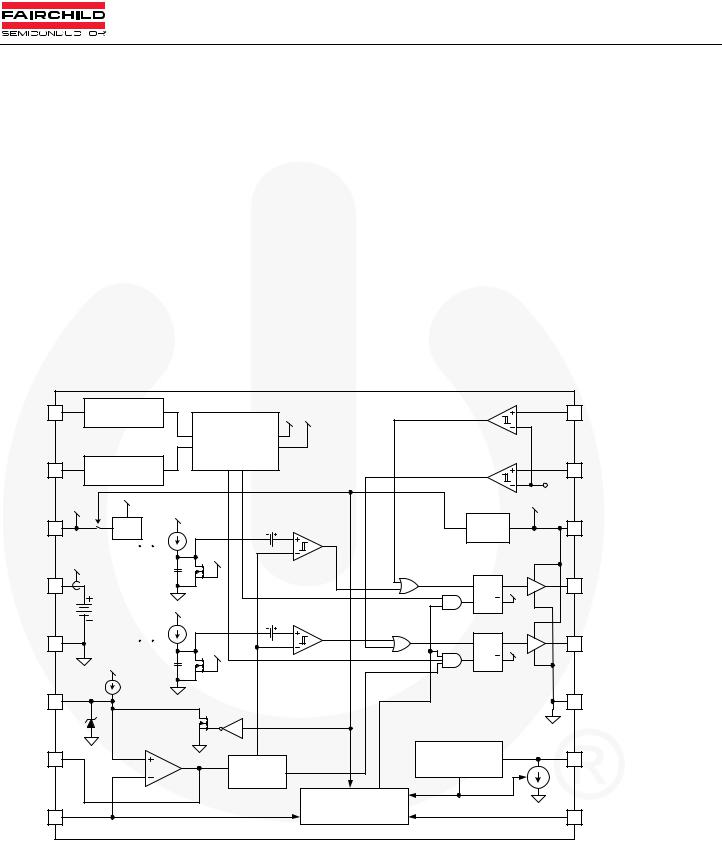
Figure 1. Block Diagram
© 2010 Fairchild Semiconductor Corporation |
4 |
FEB279_FAN9611/12 • Rev. 0.0.3 |

www.fairchildsemi.com
3. Specifications
This board has been designed and optimized for the following conditions:
Input Voltage Range |
Rated Output Power |
Output Voltage |
|
(Rated Current) |
|||
|
|
||
|
|
|
|
VIN Nominal : 85~264VAC |
400W |
400V-1A |
|
VDD Supply : 13VDC~18VDC |
|||
|
|
||
|
|
|
Note:
1.Minimum output voltage during the 20ms hold-up time is 330VDC.
VLINE = 85~264VAC
VOUT = 400V
fSW > 50kHz
Efficiency > 96% down to 20% load (115VAC)
Efficiency > 97% down to 20% load (230VAC)
PF > 0.99 at full load
The trip points for the built-in protections are set as below in the evaluation board.
The non-latching output OVP trip point is set at 108% of the nominal output voltage.
The latching output OVP trip point is set at 117% of the nominal output voltage.
The line UVLO (brownout protection) trip point is set at 68VAC (10VAC hysteresis).
The pulse-by-pulse current limit for each MOSFET is set at 9.1A.
The maximum power limit is set at ~120% of the rated output power. The phase management function permits phase shedding/adding ~15% of the nominal output power for high line (230VAC). This level can be programmed by modifying MOT resistor (R6).
© 2010 Fairchild Semiconductor Corporation |
5 |
FEB279_FAN9611/12 • Rev. 0.0.3 |

www.fairchildsemi.com
4.Test Procedure
Before testing the board; DC voltage supply for VDD, AC voltage supply for line input, and DC electric load for output should be connected to the board properly.
1.Supply VDD for the control chip first. It should be higher than 13V (refer to the specification for VDD turn-on threshold voltage in Table 1).
Table 1. |
Specification Excerpt from FAN9611/12 Datasheet |
|
|
|
|
||
|
|
|
|
|
|
|
|
Symbol |
Parameter |
Conditions |
Min. |
Typ. |
Max. |
Unit |
|
Supply |
|
|
|
|
|
|
|
|
|
|
|
|
|
|
|
ISTARTUP |
Startup Supply Current |
VDD = VON – 0.2V |
|
80 |
110 |
µA |
|
IDD |
Operating Current |
Output Not Switching |
|
3.7 |
5.2 |
mA |
|
IDD_DYM |
Dynamic Operating Current |
fSW = 50kHz; CLOAD = 2nF |
|
4 |
6 |
mA |
|
VON |
UVLO Start Threshold, FAN9611 |
VDD Increasing |
9.5 |
10.0 |
10.5 |
V |
|
|
|
|
|
|
|||
UVLO Start Threshold, FAN9612 |
12.0 |
12.5 |
13.0 |
V |
|||
|
|
||||||
|
|
|
|
|
|
|
|
VOFF |
UVLO Stop Threshold Voltage |
VDD Decreasing |
7.0 |
7.5 |
8.0 |
V |
|
VHYS |
UVLO Hysteresis, FAN9611 |
VON – VOFF |
|
2.5 |
|
V |
|
|
|
|
|
|
|||
UVLO Hysteresis, FAN9612 |
|
5.0 |
|
V |
|||
|
|
|
|
||||
|
|
|
|
|
|
|
|
2.Connect the AC voltage (85~265VAC) to start the FAN9611/12 evaluation board. Since FAN9611/12 has brownout protection, any input voltages lower than operation range triggers the protection.
3.Change load current (0~1A) and check the operation.
© 2010 Fairchild Semiconductor Corporation |
6 |
FEB279_FAN9611/12 • Rev. 0.0.3 |

www.fairchildsemi.com
5. Schematic
Figure 2. FAN9611/12 400W Evaluation Board Schematic
© 2010 Fairchild Semiconductor Corporation |
7 |
FEB388_FAN9611/12 • Rev. 0.0.3 |

www.fairchildsemi.com
6. Boost Inductor Specification
PA2975NL-5P4 from Pulse Electronics (www.pulseelectronics.com)
Core: PQ3230 (Ae=161mm2)
Bobbin: PQ3230
Inductance : 200 H
Figure 3. Boost Inductor used in this FAN9611/12 Evaluation Board
Table 2. |
Inductor Turns Specifications |
|
|
|
|
|
|
|
Pin |
|
Turns |
|
|
|
|
N1 |
5 3 |
|
30 |
|
|
|
|
Insulation Tape |
|
|
|
|
|
|
|
N2 |
2 4 |
|
3 |
Insulation Tape |
|
|
|
© 2010 Fairchild Semiconductor Corporation |
8 |
FEB388_FAN9611/12 • Rev. 0.0.3 |

www.fairchildsemi.com
7. Line Filter Inductor Specifications
A : 30mm (max)
B: 15 mm (max)
C: 11 mm
D: 13 mm
E: 15±1 mm
Electrical Specifications (1kHz, 1V)
-Inductance: 9.0mH (min.) for each winding
-DC resistance: 0.05Ω (max.) for each winding
-Number of turns: 0.9mm×2/30.5 turns for each winding
Figure 4. Line Filter Inductor Specification
Table 3. |
Materials List |
|
|
|
|
|
|
|
|
Component |
|
Material |
Manufacturer |
UL File Number |
|
|
|
|
|
Core |
|
T22x14x08 |
Core T22x14x08, TOMITA |
|
|
|
THFN-216 |
Ta Ya Electric Wire Co,. Ltd. |
E197768 |
Wire |
|
UEWN/U |
PACIFIC Wire and cable Co., Ltd. |
E201757 |
|
|
|
|
|
|
UEWE |
Tai-1 Electric Wire & Cable Co., Ltd. |
E85640 |
|
|
|
|||
|
|
UWY |
Jang Shing Wire Co., Ltd. |
E174837 |
Solder |
|
96.5%, Sn, 3%, Ag, 0.5% Cu |
Xin Yuan Co., Ltd. |
|
© 2010 Fairchild Semiconductor Corporation |
9 |
FEB388_FAN9611/12 • Rev. 0.0.3 |
 Loading...