Fairchild NC7SZ08M5X, NC7SZ08P5X, NC7SZ08FHX, NC7SZ08L6X Schematic [ru]

September 2009
NC7SZ08
TinyLogic® UHS Two-Input AND Gate
Features |
Description |
Ultra-High Speed: tPD 2.7ns (Typical) into 50pF at 5V VCC
High Output Drive: ±24mA at 3V VCC
Broad VCC Operating Range: 1.65V to 5.5V
Matches Performance of LCX Operated at 3.3V VCC
Power Down High Impedance Inputs/Outputs
Over-Voltage Tolerance inputs facilitate 5V to 3V Translation
Proprietary Noise/EMI Reduction Circuitry
Ultra-Small MicroPak™ Packages
Space-Saving SOT23 and SC70 Packages
The NC7SZ08 is a single two-input AND gate from Fairchild’s Ultra-High Speed (UHS) series of TinyLogic®. The device is fabricated with advanced CMOS technology to achieve ultra-high speed with high output drive while maintaining low static power dissipation over a broad VCC operating range. The devise is specified to operate over the 1.65V to 5.5V VCC operating range. The inputs and output are high impedance when VCC is 0V. Inputs tolerate voltages up to 6V, independent of VCC operating voltage.
Ordering Information
Part Number |
Top Mark |
Eco Status |
Package |
Packing |
|
Method |
|||||
|
|
|
|
||
|
|
|
|
|
|
NC7SZ08M5X |
7Z08 |
RoHS |
5-Lead SOT23, JEDEC MO-178 1.6mm |
3000 Units on |
|
Tape & Reel |
|||||
|
|
|
|
||
NC7SZ08P5X |
Z08 |
RoHS |
5-Lead SC70, EIAJ SC-88a, 1.25mm Wide |
3000 Units on |
|
Tape & Reel |
|||||
|
|
|
|
||
NC7SZ08L6X |
GG |
RoHS |
6-Lead MicroPak™, 1.00mm Wide |
5000 Units on |
|
Tape & Reel |
|||||
|
|
|
|
||
NC7SZ08FHX |
GG |
Green |
6-Lead, MicroPak2, 1x1mm Body, .35mm Pitch |
5000 Units on |
|
Tape & Reel |
|||||
|
|
|
|
 For Fairchild’s definition of Eco Status, please visit: http://www.fairchildsemi.com/company/green/rohs_green.html.
Gate AND Input-Two UHS ®TinyLogic — NC7SZ08
© 1996 Fairchild Semiconductor Corporation |
www.fairchildsemi.com |
NC7SZ08 • Rev. 1.0.3 |
|

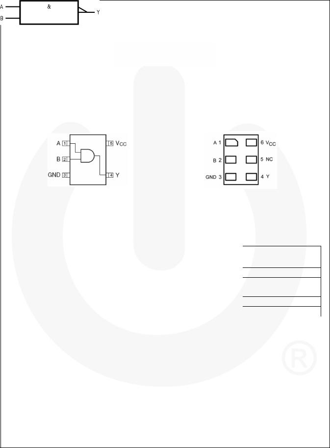
Connection Diagrams
IEEE/IEC
Figure 1. Logic Symbol
Pin Configurations
Figure 2. SC70 and SOT23 (Top View) |
Figure 3. MicroPak (Top Through View) |
Pin Definitions
Pin # SC70 / SOT23 |
Pin # MicroPak |
Name |
Description |
|
|
|
|
1 |
1 |
A |
Input |
|
|
|
|
2 |
2 |
B |
Input |
|
|
|
|
3 |
3 |
GND |
Ground |
4 |
4 |
Y |
Output |
|
|
|
|
5 |
6 |
VCC |
Supply Voltage |
|
|
|
|
|
5 |
NC |
No Connect |
Function Table
Y=AB
|
Inputs |
Output |
|
|
|
|
|
A |
|
B |
Y |
|
|
|
|
L |
|
L |
L |
|
|
|
|
L |
|
H |
L |
|
|
|
|
H |
|
L |
L |
H |
|
H |
H |
H = HIGH Logic Level
L = LOW Logic Level
Gate AND Input-Two UHS ®TinyLogic — NC7SZ08
© 1996 Fairchild Semiconductor Corporation |
www.fairchildsemi.com |
NC7SZ08 • Rev. 1.0.3 |
2 |

Absolute Maximum Ratings
Stresses exceeding the absolute maximum ratings may damage the device. The device may not function or be operable above the recommended operating conditions and stressing the parts to these levels is not recommended. In addition, extended exposure to stresses above the recommended operating conditions may affect device reliability. The absolute maximum ratings are stress ratings only.
Symbol |
Parameter |
Min. |
Max. |
Unit |
||
|
|
|
|
|
|
|
VCC |
Supply Voltage |
|
-0.5 |
6.0 |
V |
|
VIN |
DC Input Voltage |
|
-0.5 |
6.0 |
V |
|
VOUT |
DC Output Voltage |
|
-0.5 |
6.0 |
V |
|
|
|
|
|
|
|
|
IIK |
DC Input Diode Current |
|
VIN < -0.5V |
|
-50 |
mA |
|
VIN > 6.0V |
|
+20 |
|||
|
|
|
|
|
||
IOK |
DC Output Diode Current |
|
VOUT < -0.5V |
|
-50 |
mA |
|
|
|
|
|||
|
VOUT > 6V, VCC=GND |
|
+20 |
|||
|
|
|
|
|
||
|
|
|
|
|
|
|
IOUT |
DC Output Current |
|
|
±50 |
mA |
|
ICC or IGND |
DC VCC or Ground Current |
|
|
±50 |
mA |
|
|
|
|
|
|
|
|
TSTG |
Storage Temperature Range |
|
-65 |
+150 |
°C |
|
|
|
|
|
|
|
|
TJ |
Junction Temperature Under Bias |
|
|
+150 |
°C |
|
TL |
Junction Lead Temperature (Soldering, 10 Seconds) |
|
+260 |
°C |
||
|
|
|
SOT-23 |
|
200 |
|
|
|
|
|
|
|
|
PD |
Power Dissipation at +85°C |
|
SC70-5 |
|
150 |
mW |
|
MicroPak-6 |
|
130 |
|||
|
|
|
|
|
||
|
|
|
MicroPak2-6 |
|
120 |
|
|
|
|
|
|
|
|
ESD |
Human Body Model, JESD22-A114 |
|
4000 |
V |
||
Charged Device Model, JESD22-C101 |
|
2000 |
||||
|
|
|
||||
Recommended Operating Conditions
The Recommended Operating Conditions table defines the conditions for actual device operation. Recommended operating conditions are specified to ensure optimal performance to the datasheet specifications. Fairchild does not recommend exceeding them or designing to Absolute Maximum Ratings.
Symbol |
Parameter |
Conditions |
Min. |
Max. |
Unit |
|
|
|
|
|
|
VCC |
Supply Voltage Operating |
|
1.65 |
5.50 |
V |
Supply Voltage Data Retention |
|
1.50 |
5.50 |
||
|
|
|
|||
|
|
|
|
|
|
VIN |
Input Voltage |
|
0 |
5.5 |
V |
VOUT |
Output Voltage |
|
0 |
VCC |
V |
TA |
Operating Temperature |
|
-40 |
+85 |
°C |
|
|
|
|
|
|
|
|
VCC at 1.8V, 2.5V ± 0.2V |
0 |
20 |
|
tr, tf |
Input Rise and Fall Times |
VCC at 3.3V ± 0.3V |
0 |
10 |
ns/V |
|
|
VCC at 5.0V ± 0.5V |
0 |
5 |
|
|
|
|
|
|
|
|
|
SOT-23 |
|
300 |
|
|
|
|
|
|
|
θJA |
Thermal Resistance |
SC70-5 |
|
425 |
°C/W |
MicroPak-6 |
|
500 |
|||
|
|
|
|
||
|
|
|
|
|
|
|
|
MicroPak2-6 |
|
560 |
|
|
|
|
|
|
|
Note:
1.Unused inputs must be held HIGH or LOW. They may not float.
Gate AND Input-Two UHS ®TinyLogic — NC7SZ08
© 1996 Fairchild Semiconductor Corporation |
www.fairchildsemi.com |
NC7SZ08 • Rev. 1.0.3 |
3 |

DC Electrical Characteristics
Symbol |
Parameter |
VCC |
Conditions |
TA=25°C |
TA=-40 to +85°C |
Units |
||||
|
|
|
|
|
||||||
Min. |
Typ. |
Max. |
Min. |
Max. |
||||||
|
|
|
|
|
||||||
|
|
|
|
|
|
|
|
|
|
|
VIH |
HIGH Level Input |
1.65 to 1.95 |
|
0.75VCC |
|
|
0.75VCC |
|
V |
|
Voltage |
2.30 to 5.50 |
|
0.70VCC |
|
|
0.70VCC |
|
|||
|
|
|
|
|
|
|||||
|
|
|
|
|
|
|
|
|
|
|
VIL |
LOW Level Input |
1.65 to 1.95 |
|
|
|
0.25VCC |
|
0.25VCC |
V |
|
Voltage |
2.30 to 5.50 |
|
|
|
0.30VCC |
|
0.30VCC |
|||
|
|
|
|
|
|
|||||
|
|
|
|
|
|
|
|
|
|
|
|
|
1.65 |
|
1.55 |
1.65 |
|
1.55 |
|
|
|
|
|
|
|
|
|
|
|
|
|
|
|
|
1.80 |
|
1.70 |
1.80 |
|
1.70 |
|
|
|
|
|
2.30 |
VIN=VIH, IOH=-100µA |
2.20 |
2.30 |
|
2.20 |
|
|
|
|
|
|
|
|
|
|
|
|
|
|
|
|
3.00 |
|
2.90 |
3.00 |
|
2.90 |
|
|
|
VOH |
HIGH Level |
4.50 |
|
4.40 |
4.50 |
|
4.40 |
|
V |
|
Output Voltage |
1.65 |
IOH=-4mA |
1.29 |
1.52 |
|
1.29 |
|
|
||
|
|
|
|
|||||||
|
|
|
|
|
|
|
|
|
|
|
|
|
2.30 |
IOH=-8mA |
1.90 |
2.15 |
|
1.90 |
|
|
|
|
|
3.00 |
IOH=-16mA |
2.50 |
2.80 |
|
2.40 |
|
|
|
|
|
|
|
|
|
|
|
|
|
|
|
|
3.00 |
IOH=-24mA |
2.40 |
2.68 |
|
2.30 |
|
|
|
|
|
4.50 |
IOH=-32mA |
3.90 |
4.20 |
|
3.80 |
|
|
|
|
|
|
|
|
|
|
|
|
|
|
|
|
1.65 |
|
|
0.00 |
0.10 |
|
0.10 |
|
|
|
|
|
|
|
|
|
|
|
|
|
|
|
1.80 |
|
|
0.00 |
0.10 |
|
0.10 |
|
|
|
|
2.30 |
VIN=VIL, IOL=100µA |
|
0.00 |
0.10 |
|
0.10 |
|
|
|
|
|
|
|
|
|
|
|
|
|
|
|
3.00 |
|
|
0.00 |
0.10 |
|
0.10 |
|
|
VOL |
LOW Level |
4.50 |
|
|
0.00 |
0.10 |
|
0.10 |
V |
|
Output Voltage |
1.65 |
IOL=4mA |
|
0.80 |
0.24 |
|
0.24 |
|
||
|
|
|
|
|||||||
|
|
|
|
|
|
|
|
|
|
|
|
|
2.30 |
IOL=8mA |
|
0.10 |
0.30 |
|
0.30 |
|
|
|
|
3.00 |
IOL=16mA |
|
0.15 |
0.40 |
|
0.40 |
|
|
|
|
|
|
|
|
|
|
|
|
|
|
|
3.00 |
IOL=24mA |
|
0.22 |
0.55 |
|
0.55 |
|
|
|
|
4.50 |
IOL=32mA |
|
0.22 |
0.55 |
|
0.55 |
|
|
|
|
|
|
|
|
|
|
|
|
|
IIN |
Input Leakage |
0 to 5.5 |
VIN=5.5V, GND |
|
|
±1 |
|
±10 |
µA |
|
Current |
|
|
|
|||||||
|
|
|
|
|
|
|
|
|
||
IOFF |
Power Off |
0 |
VIN or VOUT=5.5V |
|
|
1 |
|
10 |
µA |
|
Leakage Current |
|
|
|
|||||||
|
|
|
|
|
|
|
|
|
||
ICC |
Quiescent Supply |
1.65 to 5.50 |
VIN=5.5V, GND |
|
|
2 |
|
20 |
µA |
|
|
Current |
|
|
|
|
|
|
|
|
|
Gate AND Input-Two UHS ®TinyLogic — NC7SZ08
© 1996 Fairchild Semiconductor Corporation |
www.fairchildsemi.com |
NC7SZ08 • Rev. 1.0.3 |
4 |
 Loading...