


MOC3031M

©2005 Fairchild Semiconductor Corporation
1
www.fairchildsemi.com
June 2005
MOC3031M, MOC3032M, MOC3033M, MOC3041M, MOC3042M, MOC3043M Rev. 1.0.1
MOC3031M, MOC3032M, MOC3033M, MOC3041M, MOC3042M, MOC3043M 6-Pin DIP Zero-Cross Optoisolators Triac Driver Output (250/400 Volt Peak)
MOC3031M, MOC3032M, MOC3033M, MOC3041M,
MOC3042M, MOC3043M
6-Pin DIP Zero-Cross Optoisolators Triac Driver Output
(250/400 Volt Peak)
Features
■
Simplifies logic control of 115 VAC power
■
Zero voltage crossing
■
dv/dt of 2000 V/µs typical, 1000 V/µs guaranteed
■
VDE recognized (File # 94766), ordering option V
(e.g., MOC3043VM)
Applications
■
Solenoid/valve controls
■
Lighting controls
■
Static power switches
■
AC motor drives
■
Temperature controls
■
E.M. contactors
■
AC motor starters
■
Solid state relays
Description
The MOC303XM and MOC304XM devices consist of a AlGaAs
infrared emitting diode optically coupled to a monolithic silicon
detector performing the function of a zero voltage crossing bilat-
eral triac driver.
They are designed for use with a triac in the interface of logic
systems to equipment powered from 115 VAC lines, such as
teletypewriters, CRTs, solid-state relays, industrial controls,
printers, motors, solenoids and consumer appliances, etc.
6
1
6
6
1
1
MAIN TERM.
NC*
N/C
*DO NOT CONNECT
(TRIAC SUBSTRATE)
1
2
3
ANODE
CATHODE
4
5
6
MAIN TERM.
ZERO
CROSSING
CIRCUIT
Schematic
查询MOC3031M供应商
2
www.fairchildsemi.com
MOC3031M, MOC3032M, MOC3033M, MOC3041M, MOC3042M, MOC3043M Rev. 1.0.1
MOC3031M, MOC3032M, MOC3033M, MOC3041M, MOC3042M, MOC3043M 6-Pin DIP Zero-Cross Optoisolators Triac Driver Output (250/400 Volt Peak)
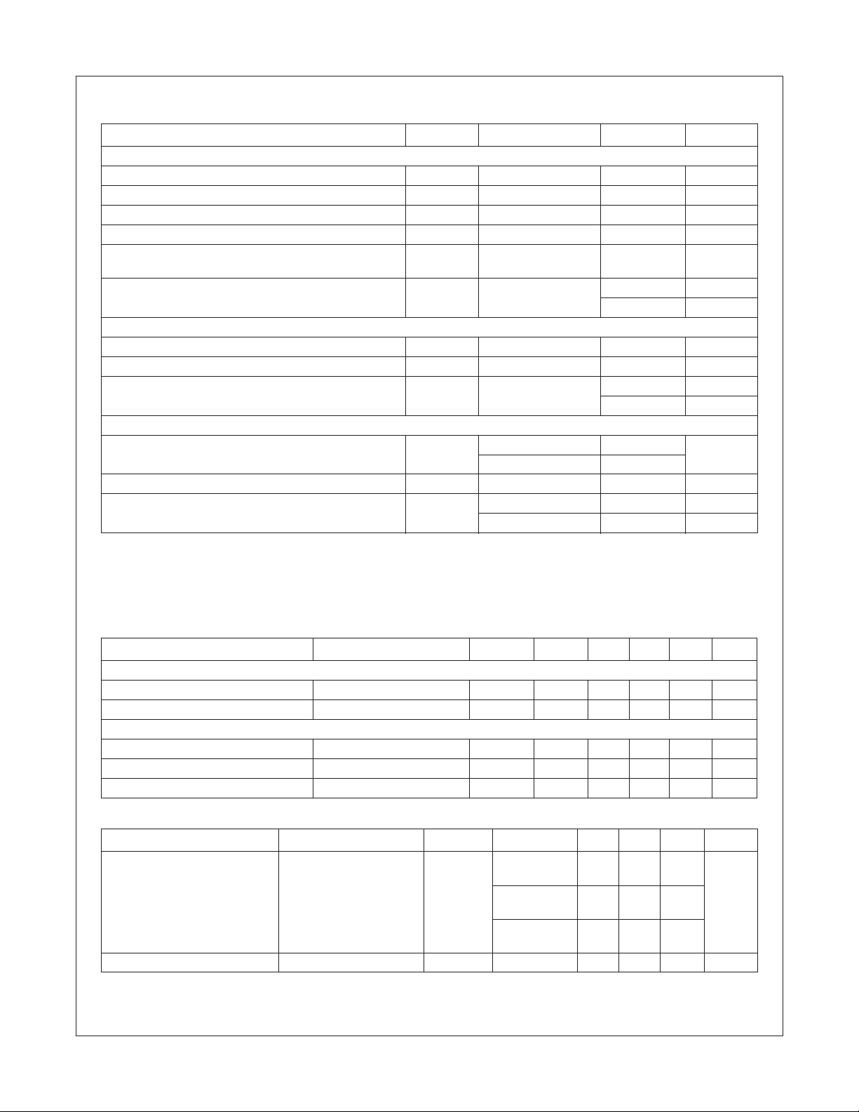
Absolute Maximum Ratings
(T
A
= 25°C unless otherwise noted)
Note
1. Isolation surge voltage, V
ISO
, is an internal device dielectric breakdown rating. For this test, Pins 1 and 2 are common, and Pins 4, 5 and 6 are
common.
Electrical Characteristics
(T
A
= 25°C Unless otherwise specified)
Individual Component Characteristics
Transfer Characteristics
(T
A
= 25°C Unless otherwise specified.)
Parameters Symbol Device Value Units
TOTAL DEVICE
Storage Temperature T
STG
All -40 to +150 °C
Operating Temperature T
OPR
All -40 to +85 °C
Lead Solder Temperature T
SOL
All 260 for 10 sec °C
Junction Temperature Range T
J
All -40 to +100 °C
Isolation Surge Voltage
(1)
(peak AC voltage, 60Hz, 1 sec duration)
V
ISO
All 7500 Vac(pk)
Total Device Power Dissipation @ 25°C
Derate above 25°C
P
D
All 250 mW
2.94 mW/°C
EMITTER
Continuous Forward Current I
F
All 60 mA
Reverse Voltage V
R
All 6 V
Total Power Dissipation 25°C Ambient
Derate above 25°C
P
D
All 120 mW
1.41 mW/°C
DETECTOR
Off-State Output Terminal Voltage V
DRM
MOC3031M/2M/3M 250 V
MOC3041M/2M/3M 400
Peak Repetitive Surge Current (PW = 100 µs, 120 pps) I
TSM
All 1 A
Total Power Dissipation @ 25°C Ambient
Derate above 25°C
P
D
All 150 mW
All 1.76 mW/°C
Parameters Test Conditions Symbol Device Min Typ Max Units
EMITTER
Input Forward Voltage I
F
= 30 mA V
F
All 1.25 1.5 V
Reverse Leakage Current V
R
= 6 V I
R
All 0.01 100 µA
DETECTOR
Peak Blocking Current, Either Direction Rated V
DRM
, I
F
= 0 (note 1) I
DRM1
All 100 nA
Peak On-State Voltage, Either Direction I
TM
= 100 mA peak, I
F
= 0 V
TM
All 1.8 3 V
Critical Rate of Rise of Off-State Voltage I
F
= 0 (Figure 9, note 3) dv/dt All 1000 V/µs
DC Characteristics Test Conditions Symbol Device Min Typ Max Units
LED Trigger Current Main terminal voltage = 3V
(note 2)
I
FT
MOC3031M/
MOC3041M
15 mA
MOC3032M/
MOC3042M
10
MOC3033M/
MOC3043M
5
Holding Current, Either Direction I
H
All 400 µA

3
www.fairchildsemi.com
MOC3031M, MOC3032M, MOC3033M, MOC3041M, MOC3042M, MOC3043M Rev. 1.0.1
MOC3031M, MOC3032M, MOC3033M, MOC3041M, MOC3042M, MOC3043M 6-Pin DIP Zero-Cross Optoisolators Triac Driver Output (250/400 Volt Peak)
Zero Crossing Characteristics
(T
A
= 25°C Unless otherwise specified.)
Note
1. Test voltage must be applied within dv/dt rating.
2. All devices are guaranteed to trigger at an I
F
value less than or equal to max I
FT
. Therefore, recommended operating I
F
lies between max I
FT
(15 mA for MOC3031M & MOC3041M, 10 mA for MOC3032M & MOC3042M, 5 mA for MOC3033M & MOC3043M) and absolute max I
F
(60 mA).
3. This is static dv/dt. See Figure 9 for test circuit. Commutating dv/dt is a function of the load-driving thyristor(s) only.
Characteristics Test Conditions Symbol Device Min Typ Max Units
Inhibit Voltage I
F
= rated I
FT
, MT1-MT2 voltage
above which device will not trigger
off-state
V
IH
All 20 V
Leakage in Inhibited State I
F
= rated I
F
, rated V
DRM
, off-state I
DRM2
All 500 µA

4
www.fairchildsemi.com
MOC3031M, MOC3032M, MOC3033M, MOC3041M, MOC3042M, MOC3043M Rev. 1.0.1
MOC3031M, MOC3032M, MOC3033M, MOC3041M, MOC3042M, MOC3043M 6-Pin DIP Zero-Cross Optoisolators Triac Driver Output (250/400 Volt Peak)
T
A
, AMBIENT TEMPERATURE (
o
C)
0.1
1
10
100
1000
10000
-40 -20 0 20 40 60 80 100
-40 -20 0 20 40 60 80 100
0.8
0.9
1.0
1.1
1.2
1.3
-
4
-
3
-
2
-
10 1234
-800
-600
-400
-200
0
200
400
600
800
I
F
- LED FORWARD CURRENT (mA)
T
A
, AMBIENT TEMPERATURE (°C)
V
TM
, ON-STATE VOLTAGE (VOLTS)
0.1 1 10 100
V
F
- FORWARD VOLT
AGE (V)
I
FT
, NORMALIZED
I
DRM
, LEAKAGE CUR
RENT (nA)
I
TM
, ON-STATE CURRENT (mA)
0.8
0.9
1.0
1.1
1.2
1.3
1.4
1.5
1.6
Figure 3. Trigger Current vs. Temperature Figure 4. Leakage Current, I
DRM
vs. Temperature
Figure 1. LED Forward Voltage vs. Forward Current Figure 2. On-State Characteristics
T
A
= -40°C
T
A
= 25°C
T
A
= 85°C
I
F
= 30mA
T
A
= 25°C
NORMALIZED TO
T
A
= 25
o
C
 Loading...