


July 2012
FAN3223 / FAN3224 / FAN3225
Dual 4A High-Speed, Low-Side Gate Drivers
Features
Industry-Standard Pinouts
4.5 to 18V Operating Range
5A Peak Sink/Source at VDD = 12V
4.3A Sink / 2.8A Source at VOUT = 6V
Choice of TTL or CMOS Input Thresholds
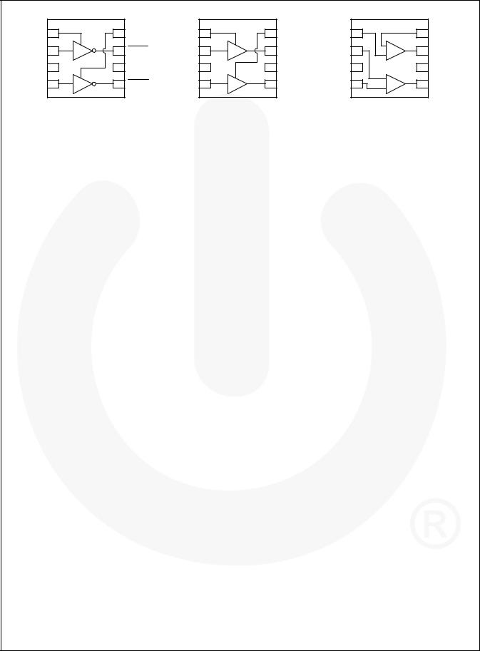
Three Versions of Dual Independent Drivers:
-Dual Inverting + Enable (FAN3223)
-Dual Non-Inverting + Enable (FAN3224)
-Dual-Inputs (FAN3225)
Internal Resistors Turn Driver Off If No Inputs
MillerDrive™ Technology
12ns / 9ns Typical Rise/Fall Times with 2.2nF Load
Typical Propagation Delay Under 20ns Matched within 1ns to the Other Channel
Double Current Capability by Paralleling Channels
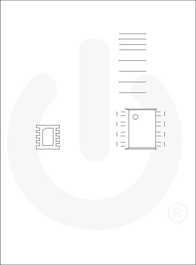
8-Lead 3x3mm MLP or 8-Lead SOIC Package
Rated from –40°C to +125°C Ambient
Applications
Switch-Mode Power Supplies
High-Efficiency MOSFET Switching
Synchronous Rectifier Circuits
DC-to-DC Converters
Motor Control
Description
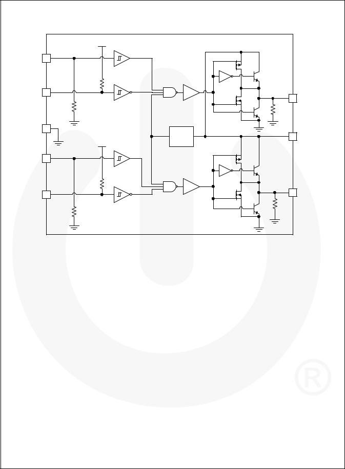
The FAN3223-25 family of dual 4A gate drivers is designed to drive N-channel enhancement-mode MOSFETs in low-side switching applications by providing high peak current pulses during the short switching intervals. The driver is available with either TTL or CMOS input thresholds. Internal circuitry provides an under-voltage lockout function by holding the output LOW until the supply voltage is within the operating range. In addition, the drivers feature matched internal propagation delays between A and B channels for applications requiring dual gate drives with critical timing, such as synchronous rectifiers. This also enables connecting two drivers in parallel to effectively double the current capability driving a single MOSFET.
The FAN322X drivers incorporate MillerDrive™ architecture for the final output stage. This bipolarMOSFET combination provides high current during the Miller plateau stage of the MOSFET turn-on / turn-off process to minimize switching loss, while providing rail- to-rail voltage swing and reverse current capability.
The FAN3223 offers two inverting drivers and the FAN3224 offers two non-inverting drivers. Each device has dual independent enable pins that default to ON if not connected. In the FAN3225, each channel has dual inputs of opposite polarity, which allows configuration as non-inverting or inverting with an optional enable function using the second input. If one or both inputs are left unconnected, internal resistors bias the inputs such that the output is pulled LOW to hold the power MOSFET OFF.
Related Resources
AN-6069 — Application Review and Comparative Evaluation of Low-Side Gate Drivers
FAN3223 |
FAN3224 |
Figure 1. Pin Configurations
FAN3225 |
Drivers Gate Side-Low Speed,-High 4A Dual — FAN3225 / FAN3224 / FAN3223
© 2007 Fairchild Semiconductor Corporation |
www.fairchildsemi.com |
FAN3223 / FAN3224 / FAN3225 • Rev. 1.0.9 |
|
Ordering Information
Part Number |
Logic |
Input |
|
Threshold |
|||
|
|
||
|
|
|
|
FAN3223CMPX |
|
CMOS |
|
FAN3223CMX |
Dual Inverting Channels + Dual Enable |
||
|
|||
FAN3223TMPX |
TTL |
||
FAN3223TMX |
|
||
|
|
||
FAN3224CMPX |
|
CMOS |
|
FAN3224CMX |
Dual Non-Inverting Channels + Dual |
||
|
|||
FAN3224TMPX |
Enable |
TTL |
|
FAN3224TMX |
|
||
|
|
||
FAN3225CMPX |
|
CMOS |
|
FAN3225CMX |
Dual Channels of Two-Input / One- |
||
|
|||
FAN3225TMPX |
Output Drivers |
TTL |
|
FAN3225TMX |
|
||
|
|
Package
3x3mm MLP-8 SOIC-8 3x3mm MLP-8 SOIC-8 3x3mm MLP-8 SOIC-8 3x3mm MLP-8 SOIC-8 3x3mm MLP-8 SOIC-8 3x3mm MLP-8 SOIC-8
Packing |
Quantity |
Method |
per Reel |
|
|
Tape & Reel |
3,000 |
Tape & Reel |
2,500 |
Tape & Reel |
3,000 |
Tape & Reel |
2,500 |
Tape & Reel |
3,000 |
Tape & Reel |
2,500 |
Tape & Reel |
3,000 |
Tape & Reel |
2,500 |
Tape & Reel |
3,000 |
Tape & Reel |
2,500 |
Tape & Reel |
3,000 |
Tape & Reel |
2,500 |
Package Outlines
Figure 2. 3x3mm MLP-8 (Top View)
Figure 3. SOIC-8 (Top View) |
Thermal Characteristics(1)
Package |
JL(2) |
JT(3) |
JA(4) |
JB(5) |
JT(6) |
Units |
8-Lead 3x3mm Molded Leadless Package (MLP) |
1.2 |
64 |
42 |
2.8 |
0.7 |
°C/W |
8-Pin Small Outline Integrated Circuit (SOIC) |
38 |
29 |
87 |
41 |
2.3 |
°C/W |
Notes:
1.Estimates derived from thermal simulation; actual values depend on the application.
2.Theta_JL ( JL): Thermal resistance between the semiconductor junction and the bottom surface of all the leads (including any thermal pad) that are typically soldered to a PCB.
3.Theta_JT ( JT): Thermal resistance between the semiconductor junction and the top surface of the package, assuming it is held at a uniform temperature by a top-side heatsink.
4.Theta_JA (ΘJA): Thermal resistance between junction and ambient, dependent on the PCB design, heat sinking, and airflow. The value given is for natural convection with no heatsink using a 2S2P board, as specified in JEDEC standards JESD51-2, JESD51-5, and JESD51-7, as appropriate.
5.Psi_JB ( JB): Thermal characterization parameter providing correlation between semiconductor junction temperature and an application circuit board reference point for the thermal environment defined in Note 4. For the MLP-8 package, the board reference is defined as the PCB copper connected to the thermal pad and protruding from either end of the package. For the SOIC-8 package, the board reference is defined as the PCB copper adjacent to pin 6.
6.Psi_JT ( JT): Thermal characterization parameter providing correlation between the semiconductor junction temperature and the center of the top of the package for the thermal environment defined in Note 4.
Drivers Gate Side-Low Speed,-High 4A Dual — FAN3225 / FAN3224 / FAN3223
© 2007 Fairchild Semiconductor Corporation |
www.fairchildsemi.com |
FAN3223 / FAN3224 / FAN3225 • Rev. 1.0.9 |
2 |
FAN3223 |
FAN3224 |
Figure 4. Pin Assignments (Repeated)
FAN3225 |
Pin Definitions
Name |
Pin Description |
|||
|
|
|
|
|
|
ENA |
Enable Input for Channel A. Pull pin LOW to inhibit driver A. ENA has TTL thresholds for both TTL and |
||
|
CMOS INx threshold. |
|||
|
|
|
||
|
|
|
|
|
|
ENB |
Enable Input for Channel B. Pull pin LOW to inhibit driver B. ENB has TTL thresholds for both TTL and |
||
|
CMOS INx threshold. |
|||
|
|
|
||
|
|
|
|
|
|
GND |
Ground. Common ground reference for input and output circuits. |
||
|
|
|
|
|
|
INA |
Input to Channel A. |
||
|
|
|
|
|
|
INA+ |
Non-Inverting Input to Channel A. Connect to VDD to enable output. |
||
|
|
|
|
|
|
INA- |
Inverting Input to Channel A. Connect to GND to enable output. |
||
|
|
|
|
|
|
INB |
Input to Channel B. |
||
|
|
|
|
|
|
INB+ |
Non-Inverting Input to Channel B. Connect to VDD to enable output. |
||
|
|
|
|
|
|
INB- |
Inverting Input to Channel B. Connect to GND to enable output. |
||
|
|
|
|
|
|
OUTA |
Gate Drive Output A: Held LOW unless required input(s) are present and VDD is above UVLO threshold. |
||
|
|
|
|
|
|
OUTB |
Gate Drive Output B: Held LOW unless required input(s) are present and VDD is above UVLO threshold. |
||
|
|
|
|
|
|
|
|
Gate Drive Output A (inverted from the input): Held LOW unless required input is present and VDD is |
|
OUTA |
||||
above UVLO threshold. |
||||
|
|
|
|
|
|
|
|
Gate Drive Output B (inverted from the input): Held LOW unless required input is present and VDD is |
|
OUTB |
||||
above UVLO threshold. |
||||
|
|
|
|
|
|
P1 |
Thermal Pad (MLP only). Exposed metal on the bottom of the package; may be left floating or connected |
||
|
to GND; NOT suitable for carrying current. |
|||
|
|
|
||
|
|
|
||
|
VDD |
Supply Voltage. Provides power to the IC. |
||
|
|
|
|
|
Output Logic
FAN3223 (x=A or B) |
|
|
|
FAN3224 (x=A or B) |
|
FAN3225 (x=A or B) |
||||||
ENx |
INx |
|
|
|
|
ENx |
INx |
OUTx |
|
INx+ |
INx− |
OUTx |
|
OUTx |
|
|
|||||||||
|
|
|
|
|
|
|
|
|
|
|
|
|
0 |
0 |
|
0 |
|
|
0 |
0(7) |
0 |
|
0(7) |
0 |
0 |
0 |
1(7) |
|
0 |
|
|
0 |
1 |
0 |
|
0(7) |
1(7) |
0 |
1(7) |
0 |
|
1 |
|
|
1(7) |
0(7) |
0 |
|
1 |
0 |
1 |
1(7) |
1(7) |
|
0 |
|
|
1(7) |
1 |
1 |
|
1 |
1(7) |
0 |
Note:
7.Default input signal if no external connection is made.
Drivers Gate Side-Low Speed,-High 4A Dual — FAN3225 / FAN3224 / FAN3223
© 2007 Fairchild Semiconductor Corporation |
www.fairchildsemi.com |
FAN3223 / FAN3224 / FAN3225 • Rev. 1.0.9 |
3 |

Block Diagrams
Figure 5. FAN3223 Block Diagram
|
|
|
|
|
|
|
|
|
|
|
|
|
|
|
|
|
|
|
|
|
|
|
|
|
|
|
|
|
|
|
|
|
|
|
|
|
|
|
|
|
|
|
|
|
|
|
|
|
|
|
|
|
|
|
|
|
|
|
|
|
|
|
|
|
|
|
|
|
|
|
|
|
|
|
|
|
|
|
|
|
|
|
|
|
|
|
|
|
|
|
|
|
|
|
|
|
|
|
|
|
|
|
|
|
|
|
|
|
|
|
|
|
|
|
|
|
|
|
|
|
|
|
|
|
|
|
|
|
|
|
|
|
|
|
|
|
|
|
|
|
|
|
|
|
|
|
|
|
|
|
|
|
|
|
|
|
|
|
|
|
|
|
|
|
|
|
|
|
|
|
|
|
|
|
|
|
|
|
|
|
|
|
|
|
|
|
|
|
|
|
|
|
|
|
|
|
|
|
|
|
|
|
|
|
|
|
|
|
|
|
|
|
|
|
|
|
|
|
|
|
|
|
|
|
|
|
|
|
|
|
|
|
|
|
|
|
|
|
|
|
|
|
|
|
|
|
|
|
|
|
|
|
|
|
|
|
|
|
|
|
|
|
|
|
|
|
|
|
|
|
|
|
|
|
|
|
|
|
|
|
|
|
|
|
|
|
|
|
|
|
|
|
|
|
|
|
|
|
|
|
|
|
|
|
|
|
|
|
|
|
|
|
|
|
|
|
|
|
|
|
|
|
|
|
|
|
|
|
|
|
|
|
|
|
|
|
|
|
|
|
|
|
|
|
|
|
|
|
|
|
|
|
|
|
|
|
|
|
|
|
|
|
|
|
|
|
|
|
|
|
|
|
|
|
|
|
|
|
|
|
|
|
|
|
|
|
|
|
|
|
|
|
|
|
|
|
|
|
|
|
|
|
|
|
|
|
|
|
|
|
|
|
|
|
|
|
|
|
|
|
|
|
|
|
|
|
|
|
|
|
|
|
|
|
|
|
|
|
|
|
|
|
|
|
|
|
|
|
|
|
|
|
|
|
|
|
|
|
|
|
|
|
|
|
|
|
|
|
|
|
|
|
|
|
|
|
|
|
|
|
|
|
|
|
|
|
|
|
|
|
|
|
|
|
|
|
|
|
|
|
|
|
|
|
|
|
|
|
|
|
|
|
|
|
|
|
|
|
|
|
|
|
|
|
|
|
|
|
|
|
|
|
|
|
|
|
|
|
|
|
|
|
|
|
|
|
|
|
|
|
|
|
|
|
|
|
|
|
|
|
|
|
|
|
|
|
|
|
|
|
|
|
|
|
|
|
|
|
|
|
|
|
|
|
|
|
|
|
|
|
|
|
|
|
|
|
|
|
|
|
|
|
|
|
|
|
|
|
|
|
|
|
|
|
|
|
|
|
|
|
|
|
|
|
|
|
|
|
|
|
|
|
|
|
|
|
|
|
|
|
|
|
|
|
|
|
|
|
|
|
|
|
|
|
|
|
|
|
|
|
|
|
|
|
|
|
|
|
|
|
|
|
|
|
|
|
|
|
|
|
|
|
|
|
|
|
|
|
|
|
|
|
|
|
|
|
|
|
|
|
|
|
|
|
|
|
|
|
|
|
|
|
|
|
|
|
|
|
|
|
|
|
|
|
|
|
|
|
|
|
|
|
|
|
|
|
|
|
|
|
|
|
|
|
|
|
|
|
|
|
|
|
|
|
|
|
|
|
|
|
|
|
|
|
|
|
|
|
|
|
|
|
|
|
|
|
|
|
|
|
|
|
|
|
|
|
|
|
|
|
|
|
|
|
|
|
|
|
|
|
|
|
|
|
|
|
|
|
|
|
|
|
|
|
|
|
|
|
|
|
|
|
|
|
|
|
|
|
|
|
|
|
|
|
|
|
|
|
|
|
|
|
|
|
|
|
|
|
|
|
|
|
|
|
|
|
|
|
|
|
|
|
|
|
|
|
|
|
|
|
|
|
|
|
|
|
|
|
|
|
|
|
|
|
|
|
|
|
|
|
|
|
|
|
|
|
|
|
|
|
|
|
|
|
|
|
|
|
|
|
|
|
|
|
|
|
|
|
|
|
|
|
|
|
|
|
|
|
|
|
|
|
|
|
|
|
|
|
|
|
|
|
|
|
|
|
|
|
|
|
|
|
|
|
|
|
|
|
|
|
|
|
|
|
|
|
|
|
|
|
|
|
|
|
|
|
|
|
|
|
|
|
|
|
|
|
|
|
|
|
|
|
|
|
|
|
|
|
|
|
|
|
|
|
|
|
|
|
|
|
|
|
|
|
|
|
|
|
|
|
|
|
|
|
|
|
|
|
|
|
|
|
|
|
|
|
|
|
|
|
|
|
|
|
|
|
|
|
|
|
|
|
|
|
|
|
|
|
|
|
|
|
|
|
|
|
|
|
|
|
|
|
|
|
|
|
|
|
|
|
|
|
|
|
|
|
|
|
|
|
|
|
|
|
|
|
|
|
|
|
|
|
|
|
|
|
|
|
|
|
|
|
|
|
|
|
|
|
|
|
|
|
|
|
|
|
|
|
|
|
|
|
|
|
|
|
|
|
|
|
|
|
|
|
|
|
|
|
|
|
|
|
|
|
|
|
|
|
|
|
|
|
|
|
|
|
|
|
|
|
|
|
|
|
|
|
|
|
|
|
|
|
|
|
|
|
|
|
|
|
|
|
|
|
|
|
|
|
|
|
|
|
|
|
|
|
|
|
|
|
|
|
|
|
|
|
|
|
|
|
|
|
|
|
|
|
|
|
|
|
|
|
|
|
|
|
|
|
|
|
|
|
|
|
|
|
|
|
|
|
|
|
|
|
|
|
|
|
|
|
|
|
|
|
|
|
|
|
|
|
|
|
|
|
|
|
|
|
|
|
|
|
|
|
|
|
|
|
|
|
|
|
|
|
|
|
|
|
|
|
|
|
|
|
|
|
|
|
|
|
|
|
|
|
|
|
|
|
|
|
|
|
|
|
|
|
|
|
|
|
|
|
|
|
|
|
|
|
|
|
|
|
|
|
|
|
|
|
|
|
|
|
|
|
|
|
|
|
|
|
|
|
|
|
|
|
|
|
|
|
|
|
|
|
|
|
|
|
|
|
|
|
|
|
|
|
|
|
|
|
|
|
|
|
|
|
|
|
|
|
|
|
|
|
|
|
|
|
|
|
|
|
|
|
|
|
|
|
|
|
|
|
|
|
|
|
|
|
|
|
|
|
|
|
|
|
|
|
|
|
|
|
|
|
|
|
|
|
|
|
|
|
|
|
|
|
|
|
|
|
|
|
|
|
|
|
|
|
|
|
|
|
|
|
|
|
|
|
|
|
|
|
|
|
|
|
|
|
|
|
|
|
|
|
|
|
|
|
|
|
|
|
|
|
|
|
|
|
|
|
|
|
|
|
|
|
|
|
|
|
|
|
|
|
|
|
|
|
|
|
|
|
|
|
|
|
|
|
|
|
|
|
|
|
|
|
|
|
|
|
|
|
|
|
|
|
|
|
|
|
|
|
|
|
|
|
|
|
|
|
|
|
|
|
|
|
|
|
|
|
|
|
|
|
|
|
|
|
|
|
|
|
|
|
|
|
|
|
|
|
|
|
|
|
|
|
|
|
|
|
|
|
|
|
|
|
|
|
|
|
|
|
|
|
|
|
|
|
|
|
|
|
|
|
|
|
|
|
|
|
|
|
|
|
|
|
|
|
|
|
|
|
|
|
|
|
|
|
|
|
|
|
|
|
|
|
|
|
|
|
|
|
|
|
|
|
|
|
|
|
|
|
|
|
|
|
|
|
|
|
|
|
|
|
|
|
|
|
|
|
|
|
|
Figure 6. FAN3224 Block Diagram |
|
|
|||||||||||||||||||||||||||||||||
© 2007 Fairchild Semiconductor Corporation |
|
|
|
|
|
|
|
|
|
|
|
|
|
|
|
|
|
|
|
|
|
|
|
|
|
|
|
|
|
|
|
|
|
|
|
|
|
|
|
|
|||||||||||||||||
FAN3223 / FAN3224 / FAN3225 • Rev. 1.0.9 |
4 |
|
|
|
|
|
|
|
|
|
|
|
|
|
|
|
|
|
|
|
|
|
|
|
|
|
|
||||||||||||||||||||||||||||||
Drivers Gate Side-Low Speed,-High 4A Dual — FAN3225 / FAN3224 / FAN3223
www.fairchildsemi.com
Block Diagrams
Figure 7. FAN3225 Block Diagram
Drivers Gate Side-Low Speed,-High 4A Dual — FAN3225 / FAN3224 / FAN3223
© 2007 Fairchild Semiconductor Corporation |
www.fairchildsemi.com |
FAN3223 / FAN3224 / FAN3225 • Rev. 1.0.9 |
5 |

Absolute Maximum Ratings
Stresses exceeding the absolute maximum ratings may damage the device. The device may not function or be operable above the recommended operating conditions and stressing the parts to these levels is not recommended. In addition, extended exposure to stresses above the recommended operating conditions may affect device reliability. The absolute maximum ratings are stress ratings only.
Symbol |
Parameter |
Min. |
Max. |
Unit |
|
|
|
|
|
VDD |
VDD to PGND |
-0.3 |
20.0 |
V |
|
|
|
|
|
VEN |
ENA and ENB to GND |
GND - 0.3 |
VDD + 0.3 |
V |
|
|
|
|
|
VIN |
INA, INA+, INA–, INB, INB+ and INB– to GND |
GND - 0.3 |
VDD + 0.3 |
V |
|
|
|
|
|
VOUT |
OUTA and OUTB to GND |
GND - 0.3 |
VDD + 0.3 |
V |
|
|
|
|
|
TL |
Lead Soldering Temperature (10 Seconds) |
|
+260 |
ºC |
|
|
|
|
|
TJ |
Junction Temperature |
-55 |
+150 |
ºC |
|
|
|
|
|
TSTG |
Storage Temperature |
-65 |
+150 |
ºC |
|
|
|
|
|
Recommended Operating Conditions
The Recommended Operating Conditions table defines the conditions for actual device operation. Recommended operating conditions are specified to ensure optimal performance to the datasheet specifications. Fairchild does not recommend exceeding them or designing to Absolute Maximum Ratings.
Symbol |
Parameter |
Min. |
Max. |
Unit |
|
|
|
|
|
VDD |
Supply Voltage Range |
4.5 |
18.0 |
V |
|
|
|
|
|
VEN |
Enable Voltage ENA and ENB |
0 |
VDD |
V |
|
|
|
|
|
VIN |
Input Voltage INA, INA+, INA–, INB, INB+ and INB– |
0 |
VDD |
V |
|
|
|
|
|
TA |
Operating Ambient Temperature |
-40 |
+125 |
ºC |
|
|
|
|
|
Drivers Gate Side-Low Speed,-High 4A Dual — FAN3225 / FAN3224 / FAN3223
© 2007 Fairchild Semiconductor Corporation |
www.fairchildsemi.com |
FAN3223 / FAN3224 / FAN3225 • Rev. 1.0.9 |
6 |

Electrical Characteristics
Unless otherwise noted, VDD=12V, TJ=-40°C to +125°C. Currents are defined as positive into the device and negative out of the device.
Symbol |
Parameter |
Conditions |
Min. |
Typ. |
Max. |
Unit |
|
|
|
|
|
|
|
Supply |
|
|
|
|
|
|
|
|
|
|
|
|
|
VDD |
Operating Range |
|
4.5 |
|
18.0 |
V |
|
|
|
|
|
|
|
IDD |
Supply Current, |
All except FAN3225C |
|
0.70 |
0.95 |
mA |
|
|
|
|
|
||
Inputs / EN Not Connected |
(8) |
|
0.21 |
0.35 |
mA |
|
|
|
|||||
|
|
FAN3225C |
|
|||
VON |
Turn-On Voltage |
INA=ENA=VDD, INB=ENB=0V |
3.5 |
3.9 |
4.3 |
V |
|
|
|
|
|
|
|
VOFF |
Turn-Off Voltage |
INA=ENA=VDD, INB=ENB=0V |
3.3 |
3.7 |
4.1 |
V |
|
|
|
|
|
|
|
Inputs (FAN322xT)(9) |
|
|
|
|
|
|
VINL_T |
INx Logic Low Threshold |
|
0.8 |
1.2 |
|
V |
|
|
|
|
|
|
|
VINH_T |
INx Logic High Threshold |
|
|
1.6 |
2.0 |
V |
|
|
|
|
|
|
|
IIN+ |
Non-inverting Input |
IN from 0 to VDD |
-1.5 |
|
175.0 |
µA |
|
|
|
|
|
|
|
IIN- |
Inverting Input |
IN from 0 to VDD |
-175.0 |
|
1.5 |
µA |
|
|
|
|
|
|
|
VHYS_T |
TTL Logic Hysteresis Voltage |
|
0.2 |
0.4 |
0.8 |
V |
|
|
|
|
|
|
|
Inputs (FAN322xC)(9) |
|
|
|
|
|
|
VINL_C |
INx Logic Low Threshold |
|
30 |
38 |
|
%VDD |
|
|
|
|
|
|
|
VINH_C |
INx Logic High Threshold |
|
|
55 |
70 |
%VDD |
|
|
|
|
|
|
|
IINL |
IN Current, Low |
IN from 0 to VDD |
-1 |
|
175 |
µA |
|
|
|
|
|
|
|
IINH |
IN Current, High |
IN from 0 to VDD |
-175 |
|
1 |
µA |
|
|
|
|
|
|
|
VHYS_C |
CMOS Logic Hysteresis Voltage |
|
|
17 |
|
%VDD |
|
|
|
|
|
|
|
ENABLE (FAN3223C, FAN3223T, FAN3224C, FAN3224T) |
|
|
|
|
||
|
|
|
|
|
|
|
VENL |
Enable Logic Low Threshold |
EN from 5V to 0V |
0.8 |
1.2 |
|
V |
|
|
|
|
|
|
|
VENH |
Enable Logic High Threshold |
EN from 0V to 5V |
|
1.6 |
2.0 |
V |
|
|
|
|
|
|
|
VHYS_T |
TTL Logic Hysteresis Voltage(10) |
|
|
0.4 |
|
V |
RPU |
Enable Pull-up Resistance(10) |
|
|
100 |
|
kΩ |
tD3 |
EN to Output Propagation Delay (11) |
0V to 5V EN, 1V/ns Slew Rate |
9 |
17 |
26 |
ns |
tD4 |
EN to Output Propagation Delay (11) |
5V to 0V EN, 1V/ns Slew Rate |
11 |
18 |
28 |
ns |
Continued on the following page…
Drivers Gate Side-Low Speed,-High 4A Dual — FAN3225 / FAN3224 / FAN3223
© 2007 Fairchild Semiconductor Corporation |
www.fairchildsemi.com |
FAN3223 / FAN3224 / FAN3225 • Rev. 1.0.9 |
7 |

Electrical Characteristics (Continued)
Unless otherwise noted, VDD=12V, TJ=-40°C to +125°C. Currents are defined as positive into the device and negative out of the device.
Symbol |
Parameter |
Conditions |
Min. |
Typ. |
Max. |
Unit |
|
|
|
|
|
|
|
Output |
|
|
|
|
|
|
|
|
|
|
|
|
|
ISINK |
OUT Current, Mid-Voltage, Sinking(10) |
OUT at VDD/2, |
|
4.3 |
|
A |
|
|
CLOAD=0.22µF, f=1kHz |
|
|
|
|
ISOURCE |
OUT Current, Mid-Voltage, Sourcing(10) |
OUT at VDD/2, |
|
-2.8 |
|
A |
|
|
CLOAD=0.22µF, f=1kHz |
|
|
|
|
IPK_SINK |
OUT Current, Peak, Sinking(10) |
CLOAD=0.22µF, f=1kHz |
|
5 |
|
A |
IPK_SOURCE |
OUT Current, Peak, Sourcing(10) |
CLOAD=0.22µF, f=1kHz |
|
-5 |
|
A |
tRISE |
Output Rise Time(11) |
CLOAD=2200pF |
|
12 |
20 |
ns |
tFALL |
Output Fall Time(11) |
CLOAD=2200pF |
|
9 |
17 |
ns |
tD1, tD2 |
Output Propagation Delay, CMOS |
0 - 12VIN, 1V/ns Slew Rate |
10 |
18 |
29 |
ns |
Inputs(12) |
||||||
tD1, tD2 |
Output Propagation Delay, TTL Inputs(12) |
0 - 5VIN, 1V/ns Slew Rate |
9 |
17 |
29 |
ns |
TDEL.MATCH |
Propagation Matching Between Channels |
INA=INB, OUTA and OUTB |
|
2 |
4 |
ns |
at 50% point |
|
|||||
IRVS |
Output Reverse Current Withstand(10) |
|
|
500 |
|
mA |
Notes: |
|
|
|
|
|
|
8.Lower supply current due to inactive TTL circuitry.
9.EN inputs have TTL thresholds; refer to the ENABLE section
10.Not tested in production.
11.See Timing Diagrams of Figure 10 and Figure 11.
12.See Timing Diagrams of Figure 8 and Figure 9.
Drivers Gate Side-Low Speed,-High 4A Dual — FAN3225 / FAN3224 / FAN3223
© 2007 Fairchild Semiconductor Corporation |
www.fairchildsemi.com |
FAN3223 / FAN3224 / FAN3225 • Rev. 1.0.9 |
8 |
 Loading...