


FAN7380
FAN7380
Half-Bridge Gate Driver
FAN7380 Half-Bridge Gate Driver
February 2007
Features
Floating Channel Designed for Bootstrapping
Operation to +600V
Typically 90mA/180mA Sourcing/Sinking Current
Driving Capability for Both Channels
Common-Mode dv/dt Noise Canceling Circuit
Extended Allowable Negative V
Signal Propagation at V
V
& VBS Supply Range from 10V to 20V
CC
UVLO Functions for Both Channels
TTL-Compatible Input Logic Threshold Levels
Matched Propagation Delay Below 50ns
Built-in 100ns Dead-Time Control Function
Output in Phase with Input Signal
CC=VBS
Swing to -9.8V for
S
=15V
Typical Applications
Fluorescent Lamp Ballast
Compact Fluorescent Lamp Ballast
Description
The FAN7380 is a monolithic half-bridge gate drive IC for
MOSFETs and IGBTs, which operate up to +600V.
Fairchild’s high-voltage process and common-mode
noise canceling technique give stable operation of highside driver under high-dv/dt noise circumstances. An
advanced level-shift circuit allows high-side gate driver
operation up to V
input logic level is compatible with standard TTL-series
logic gates. The internal shoot-through protection circuit
provides 100ns dead-time to prevent output switching
devices from both conduction during transition periods.
UVLO circuits for both channels prevent malfunction
when V
threshold voltage. Output drivers typically source/sink at
90mA/180mA, respectively, which is suitable for
fluorescent / compact fluorescent lamp ballast
applications and the systems that require low di/dt noise.
and VBS are lower than the specified
CC
=-9.8V (typical) for VBS=15V. The
S
8-SOP
Ordering Information
Device Package Pb-Free Operating Temperature Packing
FAN7380M
FAN7380MX
Note:
1. These devices passed wave soldering test by JESD22A-111.
© 2005 Fairchild Semiconductor Corporation www.fairchildsemi.com
FAN7380 Rev. 1.0.5
(1)
(1)
8-SOP Yes -40°C ~ +125°C
Tube
Tape & Reel
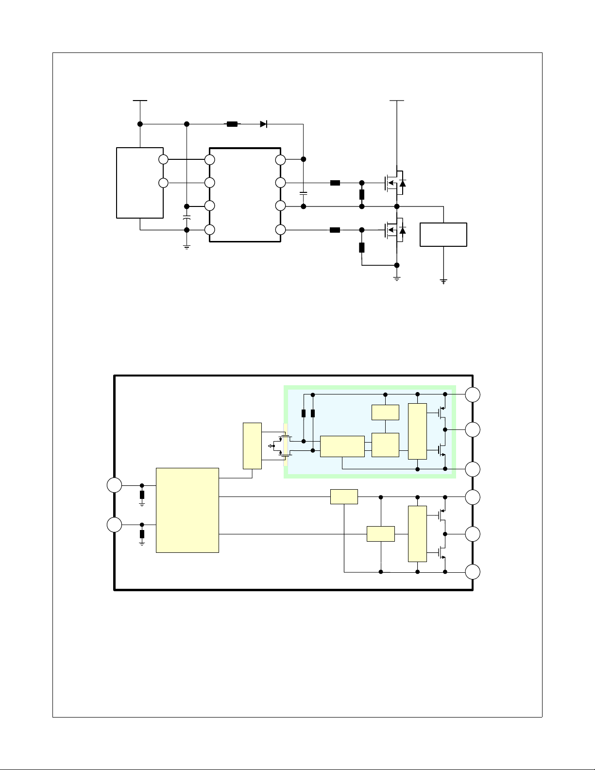
Typical Application Circuit
FAN7380 Half-Bridge Gate Driver
15V
LIN
HIN
Figure 1. Application Circuit for Fluorescent Lamp Ballast
Internal Block Diagram
C1
600V
D
R
1
LIN
2
HIN
V
3
CC
COM
4
BOOT
BOOT
HO
V
V
LO
8
B
7
6
S
5
R1
C
BOOT
R3
Q1
R2
Q2
Load
R4
FAN7380 Rev.03
HIN
LIN
8
V
B
UVLO
GENERATOR
PULSE
SCHMITT TRIGGER
2
1
INPUT
SHOOT THOUGH
PREVENTION
{DEAD-TIME=100ns}
HS(ON/OFF)
LS(ON/OFF)
NOISE
CANCELLER
UVLO
R
S
DELAY
R
DRIVER
7
HO
Q
V
6
S
3
V
CC
DRIVER
LO
5
4
COM
FAN7380 Rev.02
Figure 2. Functional Block Diagram of FAN7380
© 2005 Fairchild Semiconductor Corporation www.fairchildsemi.com
FAN7380 Rev. 1.0.5 2
Pin Configuration
FAN7380 Half-Bridge Gate Driver
LIN
HIN HO
1
2
8
7
FAN7380
V
CC
3
4COM
FAN7380 Rev.02
Figure 3. Pin Configuration (Top View)
Pin Definitions
Pin # Name I/O Description
1 LIN I Logic Input for Low-Side Gate Driver Output
2 HIN I Logic Input for High-Side Gate Driver Output
3V
4 COM Logic Ground and Low-Side Driver Return
5 LO O Low-Side Driver Output
6V
7 HO O High-Side Driver Output
8V
CC
S
B
I Low-Side Supply Voltage
I High-Voltage Floating Supply Return
I High-Side Floating Supply
6
5
V
V
LO
B
S
© 2005 Fairchild Semiconductor Corporation www.fairchildsemi.com
FAN7380 Rev. 1.0.5 3
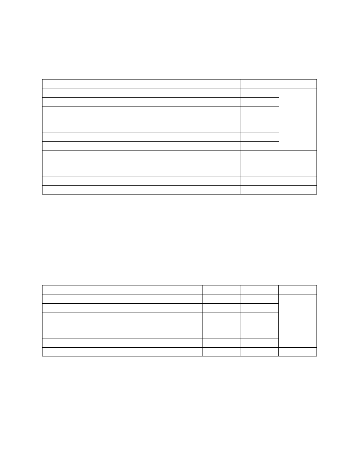
Absolute Maximum Ratings
Stresses exceeding the absolute maximum ratings may damage the device. The device may not function or be
operable above the recommended operating conditions and stressing the parts to these levels is not recommended. In
addition, extended exposure to stresses above the recommended operating conditions may affect device reliability.
The absolute maximum ratings are stress ratings only. T
Symbol Parameter Min. Max. Unit
V
S
V
B
V
HO
V
CC
V
LO
V
IN
COM Logic ground V
/dt Allowable offset voltage slew rate 50 V/ns
dV
S
(2)(3)(4)
P
D
θ
JA
T
J
T
S
Notes:
2. Mounted on 76.2 x 114.3 x 1.6mm PCB (FR-4 glass epoxy material).
3. Refer to the following standards:
JESD51-2: Integral circuits thermal test method environmental conditions - natural convection
JESD51-3: Low effective thermal conductivity test board for leaded surface mount packages
4. Do not exceed P
High-side offset voltage VB-25 VB+0.3
High-side floating supply voltage -0.3 625
High-side floating output voltage HO VS-0.3 VB+0.3
Low-side and logic-fixed supply voltage -0.3 25
Low-side output voltage LO -0.3 VCC+0.3
Logic input voltage (HIN, LIN) -0.3 VCC+0.3
Power dissipation 0.625 W
Thermal resistance, junction-to-ambient 200 °C/W
Junction temperature 150 °C
Storage temperature -50 150 °C
under any circumstances.
D
=25°C, unless otherwise specified.
A
-25 VCC+0.3
CC
V
FAN7380 Half-Bridge Gate Driver
Recommended Operating Ratings
The Recommended Operating Conditions table defines the conditions for actual device operation. Recommended
operating conditions are specified to ensure optimal performance to the datasheet specifications. Fairchild does not
recommend exceeding them or designing to Absolute Maximum Ratings.
Symbol Parameter Min. Max. Unit
V
B
V
S
V
HO
V
LO
V
IN
V
CC
T
A
High-side floating supply voltage VS+10 VS+20
High-side floating supply offset voltage 6-V
High-side (HO) output voltage V
CC
S
Low-side (LO) output voltage COM V
Logic input voltage (HIN, LIN) COM V
600
V
CC
CC
B
Low-side supply voltage 10 20
Ambient temperature -40 125 °C
V
© 2005 Fairchild Semiconductor Corporation www.fairchildsemi.com
FAN7380 Rev. 1.0.5 4
 Loading...