


ZILOG Z8E00110HEC, Z8E00110HSC, Z8E00110PEC, Z8E00110PSC, Z8E00110SEC Datasheet
...PRELIMINARY PRODUCT SPECIFICATION
1
Z8E001 |
1 |
CMOS OTP MICROCONTROLLER
FEATURES
Part |
ROM |
RAM* |
Speed |
Number |
(KB) |
(Bytes) |
(MHz) |
|
|
|
|
Z8E001 |
1 |
64 |
10 |
|
|
|
|
* General-Purpose |
|
|
|
|
|
|
|
Microcontroller Core Features
■All Instructions Execute in one 1 s Instruction Cycle with 10 MHz Crystal
■One Analog Comparator
■16-Bit Programmable Watch-Dog Timer (WDT)
■Software Programmable Timers Configurable as:
–Two 8-Bit Standard Timers and One 16-Bit Standard Timer or
–One 16-Bit Standard Timer and One 16-Bit Pulse Width Modulator (PWM) Timer
■1K x 8 On-Chip OTP EPROM Memory
■64 x 8 General-Purpose Registers (SRAM)
■Six Vectored Interrupts with Fixed Priority
■Operating Speed: DC - 10 MHz
■Six Addressing Modes: R, IR, X, D, RA, & IM
Peripheral Features
■13 Total Input/Output Pins
■One 8-Bit I/O Port (Port A)
–I/O Bit Programmable
–Each Bit Programmable as Push-Pull or OpenDrain
■One 5-Bit I/O Port (Port B)
–I/O Bit Programmable
–Includes Special Functionality: Stop-Mode Recovery Input Comparator Inputs
Selectable Edge Interrupts Timer Output
Additional Features
■On-Chip Oscillator that Accepts XTAL, Ceramic Resonator, LC, or External Clock
■Programmable Options:
–EPROM Protect
■Power Reduction Modes:
–HALT Mode with Peripheral Units Active
–STOP Mode with all Functionality Shut Down
CMOS/Technology Features
■Low-Power Consumption
■3.0V to 5.5V Operating Range @ 0°C to +70°C 4.5V to 5.5V Operating Range @ -40°C to +105°C
■18-Pin DIP,SOIC, and 20-Pin SSOP Packages.
DS97Z8X1300 |
P R E L I M I N A R Y |
1 |

Z8E001 |
|
CMOS OTP Microcontroller |
Zilog |
GENERAL DESCRIPTION
Zilog's Z8E001 Microcontroller (MCU) is a One-Time Programmable (OTP) member of Zilog’s single-chip Z8Plus MCU family that allows easy software development, debug, prototyping, and small production runs not economically desirable with masked ROM versions.
For applications demanding powerful I/O capabilities, the Z8E001's dedicated input and output lines are grouped into two ports, and are configurable under software control.
Both 8-bit and 16-bit on-chip timers, with a large number of user selectable modes, offload the system of administering real-time tasks such as counting/timing and I/O data communications.
Note: All signals with a preceding front slash, “/”, are active Low. For example, B//W (WORD is active Low); /B/W (BYTE is active Low, only).
Power connections follow conventional descriptions below:
Connection |
Circuit |
Device |
|
|
|
Power |
VCC |
VDD |
Ground |
GND |
VSS |
|
|
|
VCC GND |
|
|
|
XTAL /RESET |
||||||
|
|
|
|
|
|
|
|
|
|
|
|
|
|
|
|
|
|
|
|
|
|
|
|
|
|
|
|
|
|
|
|
|
|
|
|
|
|
|
|
|
|
Two 8-bit Timers |
|
|
|
|
|
|
|
|
|
|
|
|
|
or |
|
|
|
|
|
|
|
|
Machine Timing |
||||
One 16-bit PWM |
|
|
|
|
|
|
|
|
|||||
|
|
|
|
|
|
|
|
& Inst. Control |
|||||
Timer |
|
|
|
|
|
|
|
|
|||||
|
|
|
|
|
|
|
|
|
|
|
|
|
|
|
|
|
|
|
|
|
|
|
|
|
|
|
|
|
|
|
|
|
|
|
|
|
|
|
|
|
|
|
|
|
ALU |
|
|
|
|
|
|
|
|
||
|
|
|
|
|
|
|
|
|
|
|
|||
One 16-bit |
|
|
|
|
|
|
|
|
|
|
|
|
|
|
|
|
|
|
|
|
|
|
|
|
|
|
|
Std. Timer |
|
|
FLAG |
|
|
|
|
|
|
|
|
||
|
|
|
|
|
|
|
|
|
|
||||
|
|
|
|
|
|
|
|
|
|
|
|
|
|
|
|
|
|
|
|
|
|
|
|
|
OTP |
||
|
|
|
|
|
|
|
|
|
Prg. Memory |
||||
Interrupt |
|
|
|
|
|
||||||||
|
|
|
|
|
|
|
|
|
|
|
|
|
|
Control |
|
|
|
|
|
|
|
|
|
|
|
|
|
|
|
|
Register |
|
|
|
|
|
|
|
|
||
|
|
|
|
|
|
|
Program |
||||||
|
|
|
Pointer |
|
|
|
|
||||||
|
|
|
|
|
|
|
|
|
|
Counter |
|||
One Analog |
|
|
|
|
|
||||||||
|
|
RAM |
|
|
|
|
|
|
|
|
|||
Comparator |
|
|
|
|
|
|
|
|
|
|
|||
|
|
Register File |
|
|
|
|
|
|
|
|
|||
|
|
|
|
|
|
|
|
|
|
|
|||
|
|
|
|
|
|
|
|
|
|
|
|
|
|
|
|
|
|
|
|
|
|
|
|
|
|
|
|
|
|
|
|
|
|
|
|
|
|
|
|
|
|
|
|
|
Port A |
|
Port B |
|
|
|
|
|
|
|
I/O |
I/O |
|
|
|
|
|
|
|
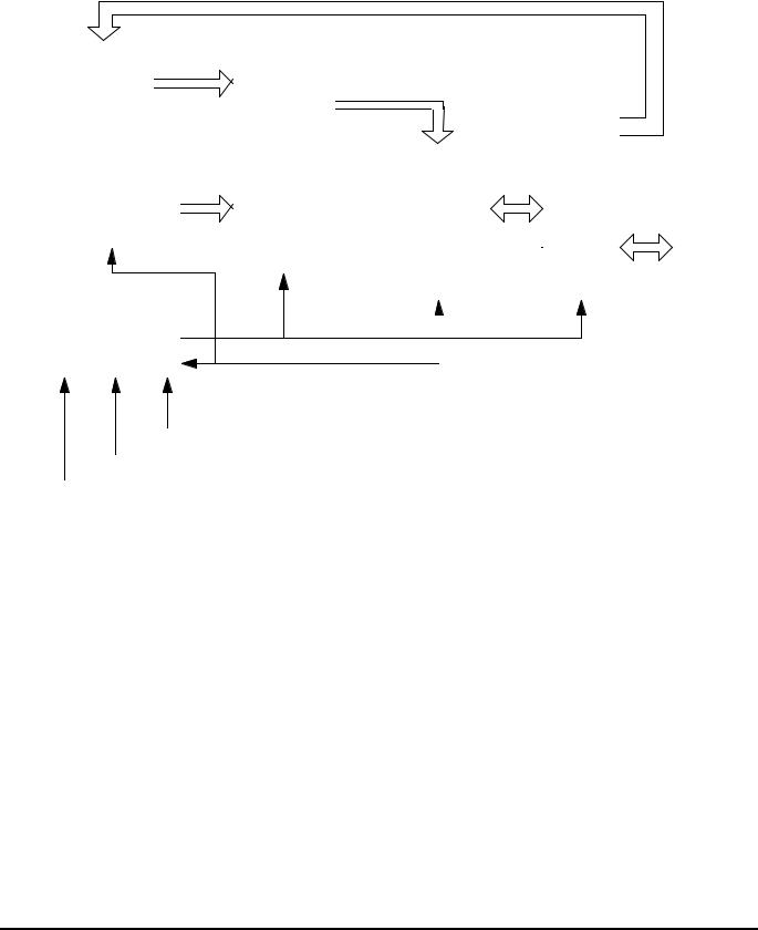
Figure 1. Functional Block Diagram |
|
|
|
|
|
2 |
|
P R E L I M I N A R Y |
DS97Z8X1300 |
|
Z8E001 |
Zilog |
CMOS OTP Microcontroller |
|
|
D7 - 0
Z8E001 MCU |
|
AD9 - 0 |
|
|
|
|
|
|
|
|
|
|
|
|
|
AD9 - 0 |
|
|
|
|
|||
|
|
|
|
ADDRESS |
|
|
|
|
|||
|
|
|
|
|
|
|
|
|
|
|
|
|
|
|
|
|
|
|
|
|
|
|
|
|
|
|
|
MUX |
|
|
|
|
DATA |
|
|
|
|
|
|
|
|
|
|
|
|
||
|
|
|
|
|
|
|
|
|
|
|
|
ADDRESS |
|
AD9 -0 |
|
|
EPROM |
D7-0 |
MUX |
|
Z8E001 |
||
|
|
|
|
|
|||||||
GENERATOR |
|
|
|
|
|
|
|
|
|||
|
|
|
|
|
|
|
D7-0 |
|
|||
|
|
|
|
|
|
|
|
|
|
|
|
|
|
|
|
|
|
|
|
|
|
|
PORT |
|
|
|
|
|
|
ROM PROT |
|
|
|
A |
|
|
|
|
|
|
|
|
|
|
|
||
|
|
|
|
|
|
OPTION BIT |
|
|
|
|
|
|
|
|
|
|
|
|
|
|
|
|
|
|
|
|
|
|
|
|
|
|
|
|
|
PGM + TEST |
|
|
|
|
|
|
|
|
|
|
|
|
|
|
|
|
|
|
|
|
|
||
MODE LOGIC |
|
|
|
|
|
|
|
|
|
|
|
|
|
|
|
|
|
|
|
|
|
||
|
|
|
|
|
|
|
|
|
|
|
|
|
|
|
|
|
|
|
|
|
|
|
|
|
|
|
|
|
|
|
|
|
|
|
|
/PGM |
ADCLR/VPP |
ADCLK
XTAL1
Figure 2. EPROM Programming Mode Block Diagram
DS97Z8X1300 |
P R E L I M I N A R Y |
3 |

Z8E001 |
|
CMOS OTP Microcontroller |
Zilog |
PIN DESCRIPTION
/PGM |
|
1 |
18 |
|
|
ADCLK |
||
|
|
|||||||
GND |
|
|
|
|
|
|
|
XTAL1 |
|
|
|
|
|
|
|
||
GND |
|
|
|
|
|
|
|
NC |
|
|
|
|
|
|
|
||
GND |
|
|
|
|
|
|
|
GND |
|
|
|
|
|
|
|
||
ADCLR/VPP |
|
|
|
DIP 18 - Pin |
|
|
|
VDD |
|
|
|
|
|
|
|
||
D7 |
|
|
|
|
|
|
|
D0 |
|
|
|
|
|
|
|
||
D6 |
|
|
|
|
|
|
|
D1 |
|
|
|
|
|
|
|
||
D5 |
|
|
9 |
10 |
|
|
D2 |
|
|
|
|
|
|||||
D4 |
|
|
|
|
D3 |
|||
|
|
|
|
|||||
|
|
|
|
|
|
|
|
|
Figure 3. 18-Pin DIP/SOIC Pin Identification/EPROM Programming Mode
Table 1. 18-Pin DIP/SOIC Pin Assignments/EPROM Programming Mode
EPROM Programming Mode |
|
|
|
Pin # |
Symbol |
Function |
Direction |
|
|
|
|
1 |
/PGM |
Prog Mode |
Input |
|
|
|
|
2-4 |
GND |
Ground |
|
|
|
|
|
5 |
ADCLR/VPP |
Clear Clk./Prog Volt. |
Input |
6-9 |
D7-D4 |
Data 7,6,5,4 |
In/Output |
|
|
|
|
10-13 |
D3-D0 |
Data 3,2,1,0 |
In/Output |
|
|
|
|
14 |
VDD |
Power Supply |
|
15 |
GND |
Ground |
|
|
|
|
|
16 |
NC |
No Connection |
|
|
|
|
|
17 |
XTAL1 |
1MHz Clock |
Input |
|
|
|
|
18 |
ADCLK |
Address Clock |
Input |
|
|
|
|
4 |
P R E L I M I N A R Y |
DS97Z8X1300 |

|
|
|
|
|
|
|
|
|
|
Z8E001 |
Zilog |
|
|
|
|
|
|
|
|
|
CMOS OTP Microcontroller |
|
|
|
|
|
|
|
|
|
|
|
|
|
|
|
|
|
|
|
|||
|
PB1 |
|
1 |
|
18 |
|
|
PBO |
||
|
|
|
||||||||
|
PB2 |
|
|
|
|
|
|
|
|
XTAL1 |
|
|
|
|
|
|
|
|
|
||
|
PB3 |
|
|
|
|
|
|
|
|
XTAL2 |
|
|
|
|
|
|
|
|
|
||
|
PB4 |
|
|
|
|
|
|
|
|
VSS |
|
|
|
|
|
|
|
|
|
||
|
/RST |
|
|
|
|
DIP 18 - Pin |
|
|
|
VCC |
|
|
|
|
|
|
|
|
|
||
|
PA7 |
|
|
|
|
|
|
|
|
PA0 |
|
|
|
|
|
|
|
|
|
||
|
PA6 |
|
|
|
|
|
|
|
|
PA1 |
|
|
|
|
|
|
|
|
|
||
|
PA5 |
|
|
|
9 |
|
10 |
|
|
PA2 |
|
|
|
|
|
|
|
||||
|
PA4 |
|
|
|
|
|
|
PA3 |
||
|
|
|
|
|
|
|||||
|
|
|
|
|
||||||
|
Figure 4. 18-Pin DIP/SOIC Pin Identification |
|||||||||
|
Table 2. 18-Pin DIP/SOIC Pin Assignments |
|||||||||
|
|
|
|
|
|
|
|
|
|
|
Standard Mode |
|
|
|
|
|
|
|
|
|
|
Pin # |
Symbol |
Function |
|
|
|
Direction |
||||
|
|
|
|
|
|
|
||||
1–4 |
PB1–PB4 |
Port B, Pins 1,2,3,4 |
|
|
|
In/Output |
||||
|
|
|
|
|
|
|
||||
5 |
/RESET |
Reset |
|
|
|
Input |
||||
|
|
|
|
|
|
|
||||
6-9 |
PA7-PA4 |
Port A, Pins 7,6,5,4 |
|
|
|
In/Output |
||||
|
|
|
|
|
|
|
||||
10-13 |
PA3-PA0 |
Port A, Pins 3,2,1,0 |
|
|
|
In/Output |
||||
|
|
|
|
|
|
|
||||
14 |
VCC |
Power Supply |
|
|
|
|
||||
15 |
VSS |
Ground |
|
|
|
|
||||
16 |
XTAL2 |
Crystal Osc. Clock |
|
|
|
Output |
||||
|
|
|
|
|
|
|
||||
17 |
XTAL1 |
Crystal Osc. Clock |
|
|
|
Input |
||||
|
|
|
|
|
|
|
||||
18 |
PB0 |
Port B, Pin 0 |
|
|
|
In/Output |
||||
|
|
|
|
|
|
|
|
|
|
|
DS97Z8X1300 |
P R E L I M I N A R Y |
5 |

Z8E001 |
|
CMOS OTP Microcontroller |
Zilog |
PIN DESCRIPTION (Continued)
|
PB1 |
|
1 |
|
20 |
|
|
PBO |
||
|
|
|
||||||||
|
PB2 |
|
|
|
|
|
|
|
|
XTAL1 |
|
|
|
|
|
|
|
|
|
||
|
PB3 |
|
|
|
|
|
|
|
|
XTAL2 |
|
|
|
|
|
|
|
|
|
||
|
PB4 |
|
|
|
|
|
|
|
|
VSS |
|
|
|
|
|
|
|
|
|
||
|
/RESET |
|
|
|
|
|
|
|
|
VCC |
|
|
|
|
SSOP 20 - Pin |
|
|
|
|||
|
NC |
|
|
|
|
|
|
|
|
NC |
|
|
|
|
|
|
|
|
|
||
|
PA7 |
|
|
|
|
|
|
|
|
PA0 |
|
|
|
|
|
|
|
|
|
||
|
PA6 |
|
|
|
|
|
|
|
|
PA1 |
|
|
|
|
|
|
|
|
|
||
|
PA5 |
|
|
|
10 |
|
11 |
|
|
PA2 |
|
|
|
|
|
|
|
||||
|
PA4 |
|
|
|
|
PA3 |
||||
|
|
|
||||||||
|
|
|
|
|
|
|||||
|
Figure 5. 20-Pin SSOP Pin Identification |
|||||||||
|
Table 3. 20-Pin SSOP Pin Assignments |
|||||||||
|
|
|
|
|
|
|
|
|
|
|
Standard Mode |
|
|
|
|
|
|
|
|
|
|
Pin # |
Symbol |
Function |
|
|
|
Direction |
||||
|
|
|
|
|
|
|
||||
1–4 |
PB1–PB4 |
Port B, Pins 1,2,3,4 |
|
|
|
In/Output |
||||
|
|
|
|
|
|
|
||||
5 |
/RESET |
Reset |
|
|
|
Input |
||||
|
|
|
|
|
|
|
||||
6 |
NC |
No Connection |
|
|
|
|
||||
|
|
|
|
|
|
|
||||
7-10 |
PA7-PA4 |
Port A, Pins 7,6,5,4 |
|
|
|
In/Output |
||||
|
|
|
|
|
|
|
||||
11-14 |
PA3-PA0 |
Port A, Pins 3,2,1,0 |
|
|
|
In/Output |
||||
|
|
|
|
|
|
|
||||
15 |
NC |
No Connection |
|
|
|
|
||||
|
|
|
|
|
|
|
||||
16 |
VCC |
Power Supply |
|
|
|
|
||||
17 |
VSS |
Ground |
|
|
|
|
||||
18 |
XTAL2 |
Crystal Osc. Clock |
|
|
|
Output |
||||
|
|
|
|
|
|
|
||||
19 |
XTAL1 |
Crystal Osc. Clock |
|
|
|
Input |
||||
|
|
|
|
|
|
|
||||
20 |
PB0 |
Port B, Pin 0 |
|
|
|
In/Output |
||||
|
|
|
|
|
|
|
|
|
|
|
6 |
P R E L I M I N A R Y |
DS97Z8X1300 |

|
Z8E001 |
Zilog |
CMOS OTP Microcontroller |
|
|
/PGM |
|
1 |
|
20 |
|
|
ADCLK |
|
|
|
|||||||
GND |
|
|
|
|
|
|
|
XTAL1 |
|
|
|
|
|
|
|
||
GND |
|
|
|
|
|
|
|
NC |
|
|
|
|
|
|
|
||
GND |
|
|
|
|
|
|
|
GND |
|
|
|
|
|
|
|
||
ADCLR/VPP |
|
|
|
|
|
|
|
NC |
|
|
SSOP 20 - Pin |
|
|
|
|||
NC |
|
|
|
|
|
|
|
VDD |
|
|
|
|
|
|
|
||
D7 |
|
|
|
|
|
|
|
NC |
|
|
|
|
|
|
|
||
D6 |
|
|
|
|
|
|
|
D1 |
|
|
|
|
|
|
|
||
D5 |
|
|
10 |
|
11 |
|
|
D2 |
|
|
|
|
|
||||
D4 |
|
|
|
|
D3 |
|||
|
|
|||||||
|
|
|
|
|
|
|
|
|
Figure 6. 20-Pin SSOP Pin Identification/EPROM Programming Mode
Table 4. 20-Pin SSOP Pin Assignments/EPROM Programming Mode
EPROM Programming Mode |
|
|
|
Pin # |
Symbol |
Function |
Direction |
|
|
|
|
1 |
/PGM |
Prog Mode |
Input |
|
|
|
|
2-4 |
GND |
Ground |
|
|
|
|
|
5 |
ADCLR/VPP |
Clear Clk./Prog Volt. |
Input |
6 |
NC |
No Connection |
|
|
|
|
|
7-10 |
D7-D4 |
Data 7,6,5,4 |
In/Output |
|
|
|
|
11-14 |
D3-D0 |
Data 3,2,1,0 |
In/Output |
|
|
|
|
15 |
NC |
No Connection |
|
|
|
|
|
16 |
VDD |
Power Supply |
|
17 |
GND |
Ground |
|
|
|
|
|
18 |
NC |
No Connection |
|
|
|
|
|
19 |
XTAL1 |
1MHz Clock |
Input |
|
|
|
|
20 |
ADCLK |
Address Clock |
Input |
|
|
|
|
DS97Z8X1300 |
P R E L I M I N A R Y |
7 |

Z8E001 |
|
|
|
|
CMOS OTP Microcontroller |
|
|
|
Zilog |
|
|
|
|
|
ABSOLUTE MAXIMUM RATINGS |
|
|
|
|
|
|
|
|
|
Parameter |
Min |
Max |
Units |
Note |
|
|
|
|
|
Ambient Temperature under Bias |
–40 |
+105 |
C |
|
|
|
|
|
|
Storage Temperature |
–65 |
+150 |
C |
|
|
|
|
|
|
Voltage on any Pin with Respect to VSS |
–0.6 |
+7 |
V |
1 |
Voltage on VDD Pin with Respect to VSS |
–0.3 |
+7 |
V |
|
Voltage on /RESET Pin with Respect to VSS |
–0.6 |
VDD+1 |
V |
2 |
Total Power Dissipation |
|
880 |
mW |
|
|
|
|
|
|
Maximum Allowable Current out of VSS |
|
80 |
mA |
|
Maximum Allowable Current into VDD |
|
80 |
mA |
|
Maximum Allowable Current into an Input Pin |
–600 |
+600 |
A |
3 |
|
|
|
|
|
Maximum Allowable Current into an Open-Drain Pin |
–600 |
+600 |
A |
4 |
|
|
|
|
|
Maximum Allowable Output Current Sunk by Any I/O Pin |
|
25 |
mA |
|
|
|
|
|
|
Maximum Allowable Output Current Sourced by Any I/O Pin |
|
25 |
mA |
|
|
|
|
|
|
Maximum Allowable Output Current Sunk by Port A |
|
40 |
mA |
|
|
|
|
|
|
Maximum Allowable Output Current Sourced by Port A |
|
40 |
mA |
|
|
|
|
|
|
Maximum Allowable Output Current Sunk by Port B |
|
40 |
mA |
|
|
|
|
|
|
Maximum Allowable Output Current Sourced by Port B |
|
40 |
mA |
|
|
|
|
|
|
Notes:
1.This applies to all pins except the /RESET pin and where otherwise noted.
2.There is no input protection diode from pin to VDD.
3.This excludes XTAL pins.
4.Device pin is not at an output Low state.
Stresses greater than those listed under Absolute Maximum Ratings may cause permanent damage to the device. This is a stress rating only; functional operation of the device at any condition above those indicated in the operational sections of these specifications is not implied. Exposure to absolute maximum rating conditions for an extended period may affect device reliability. Total power dissipation should not exceed 880 mW for the package. Power dissipation is calculated as follows:
Total Power Dissipation = |
VDD x [IDD - (sum of IOH)] |
|
+ sum of [(VDD - VOH) x IOH] |
|
+ sum of (V0L x I0L) |
8 |
P R E L I M I N A R Y |
DS97Z8X1300 |
|
Z8E001 |
Zilog |
CMOS OTP Microcontroller |
|
|
STANDARD TEST CONDITIONS
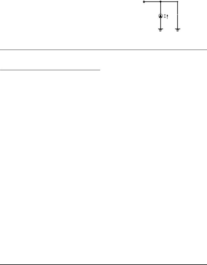
The characteristics listed below apply for standard test conditions as noted. All voltages are referenced to Ground. Positive current flows into the referenced pin (Figure 7).
From Output
Under Test
 150 pF
Figure 7. Test Load Diagram
CAPACITANCE
TA = 25°C, VCC = GND = 0V, f = 1.0 MHz, unmeasured pins returned to GND.
Parameter |
Min |
Max |
|
|
|
Input capacitance |
0 |
12 pF |
|
|
|
Output capacitance |
0 |
12 pF |
|
|
|
I/O capacitance |
0 |
12 pF |
|
|
|
DS97Z8X1300 |
P R E L I M I N A R Y |
9 |

Z8E001 |
|
|
|
|
|
|
|
|
||
CMOS OTP Microcontroller |
|
|
|
|
|
|
Zilog |
|||
|
|
|
|
|
|
|
|
|||
DC ELECTRICAL CHARACTERISTICS |
|
|
|
|
|
|
||||
|
|
|
|
|
|
|
|
|
||
|
|
|
|
T = 0°C to +70 °C Typical [1] |
|
|
|
|
||
|
|
|
|
A |
|
|
|
|
|
|
Sym |
Parameter |
VCC [3] |
Min |
Max |
@ 25°C |
Units Conditions |
Notes |
|||
|
|
|
|
|
|
|
|
|
|
|
VCH |
Clock Input High |
3.0V |
0.7VCC |
VCC+0.3 |
1.3 |
V |
Driven by External |
|
|
|
|
Voltage |
|
|
|
|
|
Clock Generator |
|
|
|
|
|
|
|
|
|
|
|
|
|
|
|
|
|
5.5V |
0.7VCC |
VCC+0.3 |
2.5 |
V |
Driven by External |
|
|
|
|
|
|
|
|
|
|
Clock Generator |
|
|
|
|
|
|
|
|
|
|
|
|
|
VCL |
Clock Input Low |
3.0V |
VSS–0.3 |
0.2VCC |
0.7 |
V |
Driven by External |
|
|
|
|
Voltage |
|
|
|
|
|
Clock Generator |
|
|
|
|
|
|
|
|
|
|
|
|
|
|
|
|
|
5.5V |
VSS–0.3 |
0.2VCC |
1.5 |
V |
Driven by External |
|
|
|
|
|
|
|
|
|
|
Clock Generator |
|
|
VIH |
Input High Voltage |
3.0V |
0.7VCC |
VCC+0.3 |
1.3 |
V |
|
|
|
|
|
|
|
5.5V |
0.7VCC |
VCC+0.3 |
2.5 |
V |
|
|
|
VIL |
Input Low Voltage |
3.0V |
VSS–0.3 |
0.2VCC |
0.7 |
V |
|
|
|
|
|
|
|
5.5V |
VSS–0.3 |
0.2VCC |
1.5 |
V |
|
|
|
VOH |
Output High Voltage |
3.0V |
VCC–0.4 |
|
3.1 |
V IOH = –2.0 mA |
|
|
||
|
|
|
5.5V |
VCC–0.4 |
|
4.8 |
V IOH = –2.0 mA |
|
|
|
VOL1 |
Output Low Voltage |
3.0V |
|
0.6 |
0.2 |
V |
IOL = +4.0 mA |
|
|
|
|
|
|
5.5V |
|
0.4 |
0.1 |
V |
IOL = +4.0 mA |
|
|
VOL2 |
Output Low Voltage |
3.0V |
|
1.2 |
0.5 |
V |
IOL = +6 mA, |
|
|
|
|
|
|
5.5V |
|
1.2 |
0.5 |
V |
IOL = +12 mA, |
|
|
VRH |
Reset Input High Voltage |
3.0V |
0.5VCC |
VCC |
1.1 |
V |
|
|
|
|
|
|
|
5.5V |
0.5VCC |
VCC |
2.2 |
V |
|
|
|
VRL |
Reset Input Low Voltage |
3.0V |
VSS–0.3 |
0.2VCC |
0.9 |
V |
|
|
|
|
|
|
|
5.5V |
VSS–0.3 |
0.2VCC |
1.4 |
V |
|
|
|
VOFFSET Comparator Input Offset |
3.0V |
|
25.0 |
10.0 |
mV |
|
|
|
||
|
Voltage |
5.5V |
|
25.0 |
10.0 |
mV |
|
|
|
|
|
|
|
|
|
|
|
|
|
|
|
IIL |
Input Leakage |
3.0V |
–1.0 |
2.0 |
0.064 |
A |
VIN = 0V, VCC |
|
|
|
|
|
|
5.5V |
–1.0 |
2.0 |
0.064 |
A |
VIN = 0V, VCC |
|
|
IOL |
Output Leakage |
3.0V |
–1.0 |
2.0 |
0.114 |
A |
VIN = 0V, VCC |
|
|
|
|
|
|
5.5V |
–1.0 |
2.0 |
0.114 |
A |
VIN = 0V, VCC |
|
|
VICR |
Comparator Input |
3.0V |
VSS–0.3 |
VCC –1.0 |
|
V |
|
7 |
|
|
|
Common Mode |
|
|
|
|
|
|
|
|
|
|
5.5V |
VSS–0.3 |
VCC –1.0 |
|
V |
|
7 |
|
||
|
Voltage Range |
|
|
|
||||||
|
|
|
|
|
|
|
|
|
||
|
|
|
|
|
|
|
|
|
|
|
IIR |
Reset Input Current |
3.0V |
-10 |
-60 |
-30 |
A |
|
|
|
|
|
|
|
5.5V |
-20 |
-180 |
-100 |
A |
|
|
|
|
|
|
|
|
|
|
|
|
|
|
|
|
|
|
|
|
|
|
|
|
|
ICC |
Supply Current |
3.0V |
|
2.5 |
2.0 |
mA |
@ 10 MHz |
4,5 |
|
|
|
|
|
5.5V |
|
6.0 |
4.0 |
mA |
@ 10 MHz |
4,5 |
|
|
|
|
|
|
|
|
|
|
|
|
ICC1 |
Standby Current |
3.0V |
|
2.0 |
1.0 |
mA |
HALT Mode VIN = 0V,VCC |
4,5 |
|
|
|
|
|
|
|
|
|
|
@ 10 MHz |
|
|
|
|
|
|
|
|
|
|
|
|
|
|
|
|
5.5V |
|
2.0 |
1.0 |
mA |
HALT Mode VIN = 0V,VCC |
4,5 |
|
|
|
|
|
|
|
|
|
@ 10 MHz |
|
|
|
|
|
|
|
|
|
|
|
|
|
10 |
P R E L I M I N A R Y |
DS97Z8X1300 |
|
|
|
|
|
|
|
Z8E001 |
Zilog |
|
|
|
|
|
CMOS OTP Microcontroller |
|
|
|
|
|
|
|
|
|
|
|
|
|
|
|
|
|
|
|
|
TA = 0 ° C to |
Typical |
|
|
|
|
|
|
+70 °C |
[1] |
|
|
|
Sym |
Parameter |
VCC [3] |
Min Max |
@ 25°C |
Units |
Conditions |
Notes |
|
|
|
|
|
|
|
|
ICC2 |
Standby Current |
3.0V |
500 |
150 |
nA |
STOP Mode VIN = 0V, VCC |
6 |
|
|
5.5V |
500 |
250 |
nA |
STOP Mode VIN = 0V,VCC |
6 |
Notes:
1.Typical values are measured at VCC = 3.3V and VCC = 5.0V.
2.VSS = 0V = GND
3.The VCC voltage specification of 3.0 V guarantees 3.3 V +/- 0.3 V and the VCC voltage specification of 5.5 V guarantees 5.0 V +/- 0.5 V.
4.All outputs unloaded, I/O pins floating, and all inputs are at VCC or VSS level.
5.CL1 = CL2 = 22 pF.
6.Same as note [4] except inputs at VCC.
7.For analog comparator input when analog comparator is enabled.
DS97Z8X1300 |
P R E L I M I N A R Y |
11 |

Z8E001 |
|
|
|
|
|
|
|
|
CMOS OTP Microcontroller |
|
|
|
|
|
|
Zilog |
|
|
|
|
|
|||||
DC ELECTRICAL CHARACTERISTICS (Continued) |
|
|
|
|||||
|
|
|
|
|
|
|
|
|
|
|
|
TA = -40°C to |
|
|
|
|
|
|
|
|
+105°C |
Typical [1] |
|
|
|
|
Sym |
Parameter |
VCC [3] |
Min |
Max |
@ 25°C |
Units |
Conditions |
Notes |
|
|
|
|
|
|
|
|
|
VCH |
Clock Input High |
4.5V |
0.7 VCC |
VCC+0.3 |
2.5 |
V |
Driven by External Clock |
|
|
Voltage |
|
|
|
|
|
Generator |
|
|
|
|
|
|
|
|
|
|
|
|
5.5V |
0.7 VCC |
VCC+0.3 |
2.5 |
V |
Driven by External Clock |
|
|
|
|
|
|
|
|
Generator |
|
|
|
|
|
|
|
|
|
|
VCL |
Clock Input Low |
4.5V |
VSS–0.3 |
0.2 VCC |
1.5 |
V |
Driven by External Clock |
|
|
Voltage |
|
|
|
|
|
Generator |
|
|
|
|
|
|
|
|
|
|
|
|
5.5V |
VSS–0.3 |
0.2 VCC |
1.5 |
V |
Driven by External Clock |
|
|
|
|
|
|
|
|
Generator |
|
|
|
|
|
|
|
|
|
|
VIH |
Input High Voltage |
4.5V |
0.7 VCC |
VCC+0.3 |
2.5 |
V |
|
|
|
|
5.5V |
0.7 VCC |
VCC+0.3 |
2.5 |
V |
|
|
VIL |
Input Low Voltage |
4.5V |
VSS–0.3 |
0.2 VCC |
1.5 |
V |
|
|
|
|
5.5V |
VSS–0.3 |
0.2 VCC |
1.5 |
V |
|
|
VOH |
Output High Voltage |
4.5V |
VCC–0.4 |
|
4.8 |
V |
IOH = –2.0 mA |
|
|
|
5.5V |
VCC–0.4 |
|
4.8 |
V |
IOH = –2.0 mA |
|
VOL1 |
Output Low Voltage |
4.5V |
|
0.4 |
0.1 |
V |
IOL = +4.0 mA |
|
|
|
5.5V |
|
0.4 |
0.1 |
V |
IOL = +4.0 mA |
|
VOL2 |
Output Low Voltage |
4.5V |
|
1.2 |
0.5 |
V |
IOL = +12 mA, |
|
|
|
5.5V |
|
1.2 |
0.5 |
V |
IOL = +12 mA, |
|
VRH |
Reset Input High |
4.5V |
0.5VCC |
VCC |
1.1 |
V |
|
|
|
Voltage |
|
|
|
|
|
|
|
|
5.5V |
0.5VCC |
VCC |
2.2 |
V |
|
|
|
|
|
|
|
|||||
VOFFSET |
Comparator Input |
4.5V |
|
25.0 |
10.0 |
mV |
|
|
|
Offset Voltage |
5.5V |
|
25.0 |
10.0 |
mV |
|
|
|
|
|
|
|
|
|
|
|
IIL |
Input Leakage |
4.5V |
-1.0 |
2.0 |
<1.0 |
A |
VIN = 0V, VCC |
|
|
|
5.5V |
-1.0 |
2.0 |
<1.0 |
A |
VIN = 0V, VCC |
|
IOL |
Output Leakage |
4.5V |
-1.0 |
2.0 |
<1.0 |
A |
VIN = 0V, VCC |
|
|
|
5.5V |
-1.0 |
2.0 |
<1.0 |
A |
VIN = 0V, VCC |
|
VICR |
Comparator Input |
4.5V |
0 |
VCC –1.5V |
|
V |
|
7 |
|
Common Mode |
|
|
|
|
|
|
|
|
5.5V |
0 |
VCC –1.5V |
|
V |
|
7 |
|
|
Voltage Range |
|
|
|||||
|
|
|
|
|
|
|
|
|
|
|
|
|
|
|
|
|
|
IIR |
Reset Input Current |
4.5V |
-18 |
-180 |
-112 |
A |
|
|
|
|
5.5V |
-18 |
-180 |
-112 |
A |
|
|
|
|
|
|
|
|
|
|
|
ICC |
Supply Current |
4.5V |
|
7.0 |
4.0 |
mA |
@ 10 MHz |
4,5 |
|
|
5.5V |
|
7.0 |
4.0 |
mA |
@ 10 MHz |
4,5 |
|
|
|
|
|
|
|
|
|
ICC1 |
Standby Current |
4.5V |
|
2.0 |
1.0 |
mA |
HALT Mode VIN = 0V, VCC |
4,5 |
|
|
|
|
|
|
|
@ 10 MHz |
|
|
|
|
|
|
|
|
|
|
|
|
5.5V |
|
2.0 |
1.0 |
mA |
HALT Mode VIN = 0V, VCC |
4,5 |
|
|
|
|
|
|
|
@ 10 MHz |
|
|
|
|
|
|
|
|
|
|
12 |
P R E L I M I N A R Y |
DS97Z8X1300 |

|
|
|
|
|
|
|
|
Z8E001 |
|
Zilog |
|
|
|
|
|
|
CMOS OTP Microcontroller |
||
|
|
|
|
|
|
|
|
|
|
|
|
|
|
|
|
|
|
|
|
|
|
|
TA = -40 °C |
Typical [1] |
|
|
|
|
|
|
|
|
to +105 °C |
|
|
|
|
||
|
|
|
|
|
|
|
|
|
|
Sym |
Parameter |
VCC[3] |
Min |
Max |
@ 25°C |
Units |
Conditions |
Notes |
|
ICC2 |
Standby Current |
4.5V |
|
700 |
250 |
nA |
STOP Mode VIN = 0V, VCC |
6 |
|
|
|
5.5V |
|
700 |
250 |
nA |
STOP Mode VIN = 0V, VCC |
6 |
|
Notes:
1.Typical values are measured at VCC = 3.3V and VCC = 5.0V.
2.VSS = 0V = GND
3.The VCC voltage specification of 3.0 V guarantees 3.3 V +/- 0.3 V and the VCC voltage specification of 5.5 V guarantees 5.0 V +/- 0.5 V.
4.All outputs unloaded, I/O pins floating, and all inputs are at VCC or VSS level.
5.CL1 = CL2 = 22 pF.
6.Same as note [4] except inputs at VCC.
7.For analog comparator input when analog comparator is enabled.
DS97Z8X1300 |
P R E L I M I N A R Y |
13 |
Z8E001 |
|
CMOS OTP Microcontroller |
Zilog |
AC ELECTRICAL CHARACTERISTICS
|
|
CLOCK |
|
|
|
1 |
|
3 |
|
|
|
|
|
|
|
|
|
|
|
|
|
|
|
|
|
|
|
|
|
||
|
|
|
|
|
|
|
2 |
|
2 |
|
|
|
|
|
|
|
|
|
|
|
|
|
|
|
|
|
|
|
|
||
|
|
|
|
|
|
|
|
|
3 |
|
|
|
|
||
|
|
IRQN |
|
|
|
|
|
|
|
|
|
||||
|
|
|
|
|
|
|
|
|
|
|
|||||
|
|
|
|
|
|
5 |
|
|
|
|
|
|
|
|
|
|
|
|
4 |
|
|
|
|
|
|
|
|
|
|
|
|
|
|
|
|
|
|
|
|
|
|
|
|
|
|
||
|
|
|
|
|
|
|
|
|
|
||||||
|
|
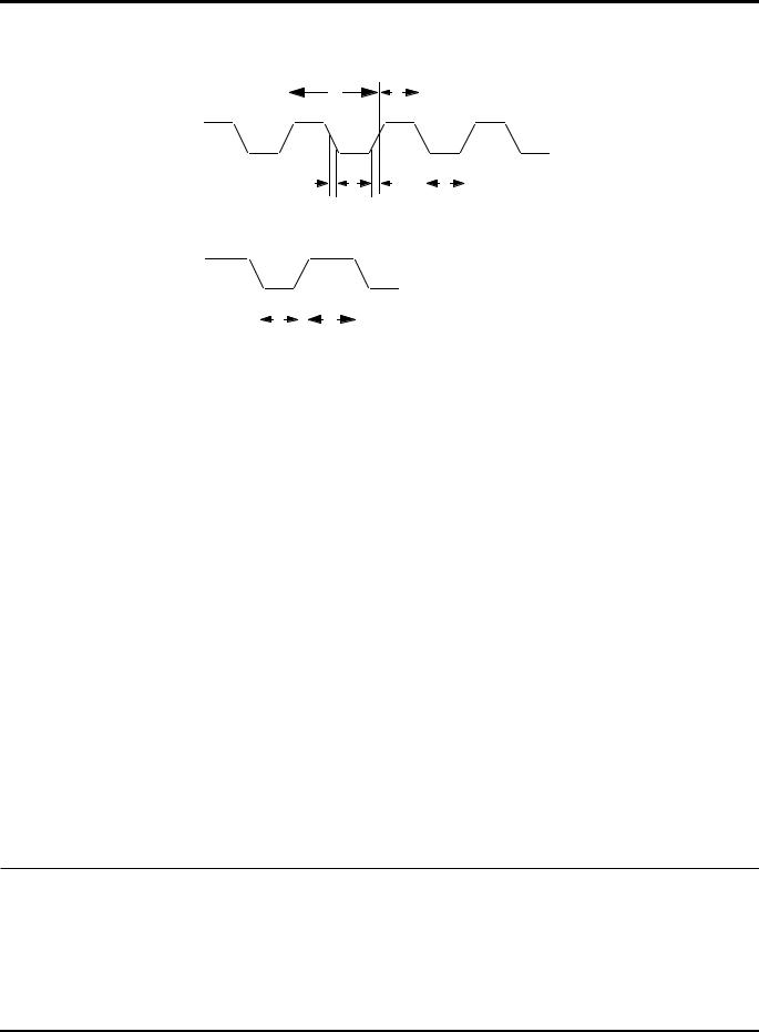
Figure 8. AC Electrical Timing Diagram |
|
|
|
||||||||||
Additional Table |
|
|
|
|
|
|
|
|
|
|
|
|
|
|
|
|
|
|
|
|
|
|
|
|
|
|
|
|
|
||
|
|
|
|
|
|
|
|
|
|
|
TA= 0 °C to +70 °C |
|
|
||
|
|
|
|
|
|
|
|
|
|
|
|
10 MHz |
|
|
|
|
|
|
|
|
|
|
|
|
VCC |
|
|
|
|
|
|
No |
Symbol |
Parameter |
|
|
[2] |
|
|
Min |
Max |
Units |
Notes |
||||
|
|
|
|
|
|
|
|
|
|
||||||
1 |
TpC |
Input Clock Period |
|
|
3.0V |
100 |
DC |
ns |
1 |
||||||
|
|
|
|
|
|
|
|
|
|
|
|
|
|
||
|
|
|
|
|
|
|
|
|
5.5V |
100 |
DC |
ns |
1 |
||
|
|
|
|
|
|
|
|
|
|||||||
2 |
TrC,TfC |
Clock Input Rise and Fall Times |
3.0V |
|
|
15 |
ns |
1 |
|||||||
|
|
|
|
|
|
|
|
|
|
|
|
|
|
|
|
|
|
|
|
|
|
|
|
|
5.5V |
|
|
15 |
ns |
1 |
|
|
|
|
|
|
|
|
|
|
|
||||||
3 |
TwC |
Input Clock Width |
|
|
3.0V |
50 |
|
ns |
1 |
||||||
|
|
|
|
|
|
|
|
|
|
|
|
|
|
||
|
|
|
|
|
|
|
|
|
5.5V |
50 |
|
ns |
1 |
||
|
|
|
|
|
|
|
|
|
|
||||||
4 |
TwIL |
Int. Request Input Low Time |
|
|
3.0V |
70 |
|
ns |
1 |
||||||
|
|
|
|
|
|
|
|
|
|
|
|
|
|
||
|
|
|
|
|
|
|
|
|
5.5V |
70 |
|
ns |
1 |
||
|
|
|
|
|
|
|
|
|
|
|
|||||
5 |
TwIH |
Int. Request Input High Time |
|
|
3.0V |
|
5TpC |
|
|
1 |
|||||
|
|
|
|
|
|
|
|
|
|
|
|
|
|
|
|
|
|
|
|
|
|
|
|
|
5.5V |
|
5TpC |
|
|
1 |
|
|
|
|
|
|
|
|
|
||||||||
6 |
Twsm |
STOP Mode Recovery Width Spec. |
3.0V |
12 |
|
ns |
|
||||||||
|
|
|
|
|
|
|
|
|
|
|
|
|
|
||
|
|
|
|
|
|
|
|
|
5.5V |
12 |
|
ns |
|
||
|
|
|
|
|
|
|
|
|
|
|
|||||
7 |
Tost |
Oscillator Start-Up Time |
|
|
3.0V |
|
|
5TpC |
|
|
|||||
|
|
|
|
|
|
|
|
|
|
|
|
|
|
|
|
|
|
|
|
|
|
|
|
|
5.5V |
|
|
5TpC |
|
|
|
|
|
|
|
|
|
|
|
|
|
|
|
|
|
|
|
Notes:
1.Timing Reference uses 0.7 VCC for a logic 1 and 0.2 VCC for a logic 0.
2.The VDD voltage specification of 3.0V guarantees 3.3V +/- 0.3V. The VDD voltage specification of 5.5V guarantees 5.0V +/- 0.5V.
14 |
P R E L I M I N A R Y |
DS97Z8X1300 |

|
Z8E001 |
Zilog |
CMOS OTP Microcontroller |
|
|
|
|
|
|
TA= –40 °C to +105 °C |
|
|
|
|
|
|
|
|
10 MHz |
|
|
|
|
|
VCC |
|
|
|
|
No |
Symbol |
Parameter |
[2] |
Min |
Max |
Units |
Notes |
|
|
|
|
|
|
|
|
1 |
TpC |
Input Clock Period |
4.5V |
100 |
DC |
ns |
1 |
|
|
|
|
|
|
|
|
|
|
|
5.5V |
100 |
DC |
ns |
1 |
|
|
|
|
|
|
|
|
2 |
TrC,TfC |
Clock Input Rise |
4.5V |
|
15 |
ns |
1 |
|
|
and Fall Times |
|
|
|
|
|
|
|
5.5V |
|
15 |
ns |
1 |
|
|
|
|
|
|
|
|
|
3 |
TwC |
Input Clock Width |
4.5V |
50 |
|
ns |
1 |
|
|
|
|
|
|
|
|
|
|
|
5.5V |
50 |
|
ns |
1 |
|
|
|
|
|
|
|
|
4 |
TwIL |
Int. Request Input |
4.5V |
70 |
|
ns |
1 |
|
|
Low Time |
|
|
|
|
|
|
|
5.5V |
70 |
|
ns |
1 |
|
|
|
|
|
|
|
|
|
5 |
TwIH |
Int. Request Input |
4.5V |
5TpC |
|
|
1 |
|
|
High Time |
|
|
|
|
|
|
|
5.5V |
5TpC |
|
|
1 |
|
|
|
|
|
|
|
|
|
6 |
Twsm |
STOP Mode Recovery |
4.5V |
12 |
|
ns |
|
|
|
Width Spec. |
|
|
|
|
|
|
|
5.5V |
12 |
|
ns |
|
|
|
|
|
|
|
|
|
|
7 |
Tost |
Oscillator Start-Up Time |
4.5V |
|
5TpC |
|
|
|
|
|
|
|
|
|
|
|
|
|
5.5V |
|
5TpC |
|
|
|
|
|
|
|
|
|
|
Notes:
1.Timing Reference uses 0.7 VCC for a logic 1 and 0.2 VCC for a logic 0.
2.The VDD voltage specification of 3.0V guarantees 3.3V +/- 0.3V. The VDD voltage specification of 5.5V guarantees 5.0V +/- 0.5V.
DS97Z8X1300 |
P R E L I M I N A R Y |
15 |
 Loading...