


Z80380

DC-8297-03
PREFACE
Thank you for your interest in the Z380
™
Central Processing Unit (CPU) and its
associated family of products. This Technical Manual describes programming
and operation of the Z380
™
Superintegration
™
Core CPU, which is found in the
Z380 Microprocessor Unit (MPU), and products built around Z380
™
CPU core.
This Z380 User's Manual consists of the following Sections:
1. Z380
™
Architectural Overview
Chapter 1 is an introductory section covering the key features and
giving an overview of the architecture of the device.
2. Address Spaces
Chapter 2 explains the address spaces the Z380 CPU can handle.
Also, this chapter includes a brief description of the on-chip regis-
ters.
3. Native/Extended Mode, Word/Long Word Mode of Operation,
and Decoder Directives
This chapter provides a detailed explanation on the Z380’s unique
features, operation modes, and the Decoder Directives.
4. Addressing Modes and Data Types
Chapter 4 describes the Addressing mode and data types which the
Z380 can handle.
5. Instruction Set
Chapter 5 contains an overview of the instruction set; as well as a
detailed instruction-by-instruction description in alphabetical order.
6. Interrupts and Traps
Chapter 6 explains the interrupts and traps features of the Z380.
7. Reset
Chapter 7 describes the Reset function.
8. Z380 Benchmark Appnote
9. Z380 Questions & Answers
Z80380 CPU
U
SER'S MANUAL

ZILOG
DC-8297-03
Appendix A
Appendix A covers the Z380’s instruction format.
Appendix B
Appendix B contains all Z380 instructions sorted in Alphabetical
Order.
Appendix C
Appendix C contains all Z380 instructions sorted in Numerical
Order.
Appendix D
The Tables in Appendix D lists all the Z380 instructions in instruction
affected by Native/Extended mode and Word/Long Word mode.
Appendix E
The Tables in Appendix E lists all the Z380 instructions in instruction
affected by DDIR IM (Immediate Decoder Directives) mode.
Index
A to Z listing of Z380
™
User's Manual key words and phrases.
This manual assumes the reader has a basic knowledge of CPU-
based system architectures and software development systems,
such as the use of the text editor, and invoking the assembler/
compiler. Also, knowledge of the Z80
®
CPU architecture is desirable.
Zilog’s products are not authorized for use as critical compo-
nents in life support devices or systems unless a specific written
agreement pertaining to such intended use is executed between
the customer and Zilog prior to use. Life support devices or
systems are those which are intended for surgical implantation
into the body, or which sustains life whose failure to perform,
when properly used in accordance with instructions for use
provided in the labeling, can be reasonably expected to result in
significant injury to the user.
Zilog, Inc. 210 East Hacienda Ave.
Campbell, CA 95008-6600
Telephone (408) 370-8000
Telex 910-338-7621
FAX 408 370-8056
Internet: http://www.zilog.com
© 1994, 1995, 1996, 1997 by Zilog, Inc. All rights reserved. No
part of this document may be copied or reproduced in any form
or by any means without the prior written consent of Zilog, Inc.
The information in this document is subject to change without
notice. Devices sold by Zilog, Inc. are covered by warranty and
patent indemnification provisions appearing in Zilog, Inc. Terms
and Conditions of Sale only.
ZILOG, INC. MAKES NO WARRANTY, EXPRESS, STATUTORY,
IMPLIED OR BY DESCRIPTION, REGARDING THE INFORMA-
TION SET FORTH HEREIN OR REGARDING THE FREEDOM OF
THE DESCRIBED DEVICES FROM INTELLECTUAL PROPERTY
INFRINGEMENT. ZILOG, INC. MAKES NO WARRANTY OF MER-
CHANTABILITY OR FITNESS FOR ANY PURPOSE.
Zilog, Inc. shall not be responsible for any errors that may appear
in this document. Zilog, Inc. makes no commitment to update or
keep current the information contained in this document.

U
SER
'
S
M
ANUAL
Z
ILOG
1.1 INTRODUCTION
USER’s MANUAL
CHAPTER 1
Z380
™
ARCHITECTURAL OVERVIEW
The Z380 CPU incorporates advanced architectural fea-
tures that allow fast and efficient throughput and increased
memory addressing capabilities while maintaining Z80
®
CPU and Z180
®
MPU object-code compatibility. The Z380
CPU core provides a continuing growth path for present
Z80- or Z180
®
-based designs and offers the following key
features:
■ Full Static CMOS Design with Low Power Standby
Mode Support
■ DC to 18 MHz Operating Frequency @ 5 Volts V
CC
■ DC to 10 MHz Operating Frequency @ 33 Volts V
CC
■ Enhanced Instruction Set that Maintains Object-Code
Compatibility with Z80 and Z180 Microprocessors
■ 16-Bit (64K) or 32-Bit (4G) Linear Address Space
■ 16-Bit Internal Data Bus
■ Two Clock Cycle Instruction Execution (Minimum)
■ Multiple On-Chip Register Files (Z380 MPU has Four
Banks)
■ BC/DE/HL/IX/IY Registers are Augmented by 16-Bit
Extended Registers (BCz/DEz/HLz/IXz/IYz), PC/SP/I
Registers are Augmented by Extended Registers (PCz/
SPz/Iz) for 32-Bit Addressing Capability.
■ Newly Added IX’ and IY’ Registers with Extended
Registers (IXz’/IYz’)
■ Enhanced Interrupt Capabilities, Including 16-Bit
Vector
■ Undefined Opcode Trap for Full Z380 CPU Instruction
Set
The Z380 CPU, an enhanced version of the Z80 CPU,
retains the Z80 CPU instruction set to maintain complete
binary-code compatiblity with present Z80 and Z180 codes.
The basic addressing modes of the Z80 microprocessor
have been augmented with Stack Pointer Relative loads
and stores, 16-bit and 24-bit Indexed offsets, and in-
creased Indirect register addressing flexibility, with all of
the addressing modes allowing access to the entire 32-bit
address space. Significant additions have been made to
the instruction set iincorporating16-bit arithmetic and logi-
cal operations, 16-bit I/O operations, multiply and divide,
a complete set of register-to-register loads and exchanges,
plus 32-bit load and exchange, and 32-bit arithmetic
operation for address calculation.
The basic register file of the Z80 microprocessor is ex-
panded to include alternate register versions of the IX and
IY registers. There are four sets of this basic Z80 micropro-
cessor register file present in the Z380 MPU, along with the
necessary resources to manage switching between the
different register sets. All of the register pairs and index
registers in the basic Z80 microprocessor register file are
expanded to 32 bits.
The Z380 CPU expands the basic 64 Kbyte Z80 and Z180
address space to a full 4 Gbyte (32-bit) address space.
This address space is linear and completely accessible to
the user program. The external I/O address space is
similarly expanded to a full 4 Gbyte (32-bit) range, and 16-
bit I/O, both simple and block move are included. A 256
byte-wide internal I/O space has been added. This space
will be used to access on-chip I/O resources on future
Superintegration implementation of this CPU core.
Figure 1-1 provides a detailed description of the basic
register architecture of the Z380 CPU with the size of the
register banks shown at four each, however, the Z380 CPU
architecture allows future expansion of up to 128 sets of
each.
1-2
Z380
™
USER'S MANUAL
DC-8297-03
ZILOG
1.1 INTRODUCTION (Continued)
AF
BC
DE
HL
IXU IXL
IYU IYL
A' F'
B' C'
D' E'
H' L'
IXU' IXL'
IYU' IYL'
BCz'
DEz'
HLz'
IXz'
IYz'
BCz
DEz
HLz
IXz
IYz
R
I
SPz
PCz
Iz
SP
PC
4 Sets of Registers
Figure 1-1. Z380
™
CPU Register Architecture

1-3
Z380
™
USER'S MANUAL
ZILOG
DC-8297-03
1.2 CPU ARCHITECTURE
The Z380 CPU is a binary-compatible extension of the Z80
CPU and the Z180 CPU architecture. High throughput
rates are achieved by a high clock rate, high bus band-
width, and instruction fetch/execute overlap. Communi-
cating to the external world through an 8-bit or 16-bit data
bus, the Z380 CPU is a full 32-bit machine internally, with
a 32-bit ALU and 32-bit registers.
1.2.1 Modes of Operation
To maintain compatibility with the Z80/Z180 CPU while
having the capability to manipulate 4 Gbytes of memory
address range, the Z380 CPU has two bits in the Select
Register (SR) to control the modes of operation. One bit
controls the address manipulation mode: Native mode or
Extended mode; and the other bit controls the data ma-
nipulation mode: Word mode or Long Word mode. In
result, the Z380 CPU has four modes of operation. On
reset, the Z380 CPU is in Native/Word mode, which is
compatible to the Z80/Z180’s operation mode. For details
on this subject, refer to Chapter 3, “Native/Extended Mode,
Word/Long Word Mode of Operation, and Decoder Direc-
tive Instructions.”
1.2.1.1 Native Mode and Extended Mode
The Z380 CPU can operate in either Native or Extended
mode, as controlled by a bit in the Select Register (SR). In
Native mode (the Reset configuration), all address ma-
nipulations are performed modulo 65536 (2
16
). In this
mode, the Program Counter (PC) only increments across
16 bits, all address manipulation instructions (increment,
decrement, add, subtract, indexed, stack relative, and PC
relative) only operate on 16 bits, and the Stack Pointer (SP)
only increments and decrements across 16 bits. The PC
high-order word is left at all zeros, as the high-order words
of the SP and the I register. Thus, Native mode is fully
compatible with the Z80 CPU’s 64 Kbyte address mode. It
is still possible to address memory outside of 64 Kbyte
address space for data storage and retrieval in Native
mode, however, since direct addresses, indirect addresses,
and the high-order word of the SP, I, and the IX and IY
registers may be loaded with non-zero values. Executed
code and interrupt service routines must reside in the
lowest 64 Kbytes of the address space.
In Extended mode, however, all address manipulation
instructions operate on 32 bits, allowing access to the
entire 4 Gbyte address space of the Z380 CPU. In both
Native and Extended modes, the Z380 drives all 32 bits of
the address onto the external address bus; only the width
of the manipulated addresses distinguishes Native from
Extended mode. The Z380 CPU implements one instruc-
tion to allow switching from Native to Extended mode
(SETC XM); however, once in Extended mode, only Reset
will return the Z380 CPU to Native mode. This restriction
applies because of the possibility of “misplacing” interrupt
service routines or vector tables during the transition from
Extended mode back to Native mode.
1.2.1.2 Word or Long Word Mode
In addition to Native and Extended mode, which are
specific to memory space addressing, the Z380 CPU can
operate in either Word or Long Word mode specific to data
load and exchange operations. In Word mode (the Reset
configuration), all word load and exchange operations
manipulate 16-bit quantities. For example, only the low-
order words of the source and destination are exchanged
in an exchange operation, with the high-order words
unaffected.
In the Long Word mode, all 32 bits of the source and
destination are exchanged. The Z380 CPU implements
two instructions plus decoder directives to allow switching
between Word and Long Word mode; SETC LW (Set
Control Long Word) and RESC LW (Reset Control Long
Word) perform a global switch, while DDIR W, DDIR LW
and their variants are decoder directives that select a
particular mode only for the instruction that they precede.
Note that all word data arithmetic (as opposed to address
manipulation arithmetic), rotate, shift, and logical opera-
tions are always in 16-bit quantities. They are not con-
trolled by either the Native/Extended or Word/Long Word
selections. The exceptions to the 16-bit quantities are, of
course, those multiply and divide operations with 32-bit
products or dividends.
All word Input/Output operations are performed on 16-bit
values, regardless of Word/Long Word operation.
1.2.2 Address Spaces
Addressing spaces in the Z380 CPU include the CPU
register, the CPU control register, the memory address,
on-chip I/O address, and the external I/O address. The
CPU register space is a superset of the Z80 CPU register
set, and consists of all of the registers in the CPU register
file. These CPU registers are used for data and address
manipulation, and are an extension of the Z80 CPU register
set, with four sets of this extended Z80 CPU register set
present in the Z380 CPU. Access to these registers is
specified in the instruction, with the active register set
selected by bits in the Select Register (SR) in the CPU
control register space.

1-4
Z380
™
USER'S MANUAL
DC-8297-03
ZILOG
1.2.2 Address Spaces (Continued)
Each register set includes the primary registers A, F, B, C,
D, E, H, L, IX, and IY, as well as the alternate registers A’,
F’, B’, C’, D’, E’, H’, L’, IX’, and IY’. Also, IX, IX’, IY, and IY’
registers are accessible as two byte registers, each named
as IXU, IXL, IXU’ IXL’, IYU, IYL, IYU’, and IYL’. These byte
registers can be paired B with C, D with E, H with L, B’ with
C’, D’ with E’, and H’ with L’ to form word registers, and
these word registers are extended to 32 bits with the “z”
extension to the register. This register extension is only
accessible when using the register as a 32-bit register (in
the Long Word mode) or when swapping between the
most-significant and least-significant word of a 32-bit
register using SWAP instructions. Whenever an instruction
refers to a word register, the implicit size is controlled by
Word or Long Word mode. Also included are the R, I, and
SP registers, as well as the PC.
The Select Register (SR) determines the operation of the
Z380 CPU. The contents of this register determine the CPU
operating mode, which register bank will be used, the
interrupt mode in effect, and so on.
The Z380 CPU’s memory address space is linear 4 Gbytes.
To keep compatibility with the Z80 CPU memory address-
ing model, it has two control bits to change its operation
modes—Native or Extended, Word or Long Word.
The Z380 CPU architecture also distinguishes between
the memory and I/O addressing space and, therefore,
requires specific I/O instructions. Furthermore, I/O ad-
dressing space is subdivided into the on-chip I/O address
space and the external I/O addressing space. External
I/O addressing space in the Z380 CPU is 32 bits long, and
internal I/O addressing space is 8-bits long. There are
separate sets of I/O instructions for each I/O addressing
space.
Some of the Internal I/O registers are used to control the
functionality of the device, such as to program/read status
of Trap, Assigned Vector Base address, enabling of inter-
rupts, and to get Chip version ID.
For details on this topic, refer to Chapter 2, “Address
Spaces.”
1.2.3 Data Types
Many data types are supported by the Z380 CPU architec-
ture. The basic data type is the 8-bit byte, which is also the
basic addressable memory element. The architecture also
supports operations on bits, BCD (Binary Coded Decimal)
digits, words (16 bits or 32 bits), byte strings and word
strings. For details on this topic, refer to Section 4.3, “Data
Types.”
1.2.4. Addressing Modes
Addressing modes are used by the Z380 CPU to calculate
the effective address of an operand needed for execution
of an instruction. Seven addressing modes are supported
by the Z380 CPU. Of these seven, one is an addition to the
Z80 CPU addressing modes (Stack Pointer Relative) and
the remaining six modes are either existing or extensions
to Z80 CPU addressing modes.
■ Register
■ Immediate
■ Indirect Register
■ Direct Address
■ Indexed
■ Program Counter Relative
■ Stack Pointer Relative
All addressing modes are available on the 8-bit load,
arithmetic, and logical instructions; the 8-bit shift, rotate,
and bit manipulation instructions are limited to the regis-
ters and Indirect register addressing modes. The 16-bit
loads on the addressing registers support all addressing
modes except Index, while other 16-bit operations are
limited to the Register, Immediate, Indirect Register, In-
dex, Direct Address, and PC Relative addressing modes.
For details on this subject, refer to Chapter 4, “Addressing
Modes and Data Types.”
1.2.5. Instruction Set
The Z380 CPU instruction set is an expansion of the Z80
instruction set; the enhancements include support for
additional addressing modes for the Z80 instructions as
well as the addition of new instructions. The Z380 CPU
instruction set provides a full complement of 8-bit, 16-bit,
and 32-bit operation, including multiplication and division.
For details on this subject, refer to Chapter 5, “Instruction
Set.”
1.2.6 Exception Conditions
The Z380 CPU supports three types of exceptions (condi-
tions that alter the normal flow of program execution);
interrupts, traps, and resets.
Interrupts are asynchronous events typically triggered by
peripherals requiring attention. The Z380 CPU interrupt
structure has been significantly enhanced by increasing
the number of interrupt request lines and by adding an
efficient means for handling nested interrupts. The Z380
CPU has five interrupt lines. These are: Nonmaskable
Interrupt line (/NMI) and Maskable interrupt lines (/INT0,
/INT1, /INT2, and /INT3). Interrupt requests on /INT3-/INT1

1-5
Z380
™
USER'S MANUAL
ZILOG
DC-8297-03
are handled by a newly added interrupt handing mode,
“Assigned Vectored Mode,” which is a fixed vectored
interrupt mode similar in interrupt handling to the Z180’s
interrupts from on-chip peripherals. For handling interrupt
requests on the /INT0 line, there are four modes available:
■ 8080 compatible (Mode 0), in which the interrupting
device provides the first instruction of the interrupt
routine.
■ Dedicated interrupts (Mode 1), in which the CPU
jumps to a dedicated address when an interrupt
occurs.
■ Vectored interrupt mode (Mode 2), in which the
interrupting peripheral device provides a vector into a
table of jump address.
■ Enhanced vectored interrupt mode (Mode 3), wherein
the CPU expects 16-bit vector, instead of 8-bit interrupt
vectors in Mode 2.
The first three modes are compatible with Z80 interrupt
modes; the fourth mode provides more flexibility.
Traps are synchronous events that trigger a special CPU
response when an undefined instruction is executed. It
can be used to increase system reliability, or used as a
“software trap instruction.”
Hardware resets occur when the /RESET line is activated
and override all other conditions. A /RESET causes certain
CPU control registers to be initialized.
For details on this subject, refer to Chapter 6, “Interrupts
and Traps.”
1.3 BENEFITS OF THE ARCHITECTURE
The Z380 CPU architecture provides several significant
benefits, including increased program throughput achieved
by higher bus bandwidth (16-bit wide bus), reduction to
two clocks/basic machine cycle (vs four clocks/cycle on
the Z80 CPU), prefetch cue, access to the larger linear
addressing space, enhanced instructions/new address-
ing mode, data/address manipulation in 16/32 bits, and
faster context switching by utilizing multiple register banks.
1.3.1 High Throughput
Very high throughput rates can be achieved with the Z380
CPU, due to the basic machine cycle’s reduction to two
clocks/cycle from four clocks/cycle on the Z80 CPU, fine
tuned four staged pipeline with prefetch cue. This well
designed pipeline and prefetch cue are both totally trans-
parent to the user, thus maximizing the efficiency of the
pipeline all the time. The Z380 CPU implemented onto the
Z380 MPU is configured with a 16-bit wide data bus, which
doubles the bus bandwidth. These architectural features
result in two clocks/instructions execution minimum, three
clocks/instruction on average. The high clock rates (up to
40 MHz) achievable with this processor. Make the overall
performance of the Z380 CPU more than ten times that of
the Z80.
1.3.2 Linear Memory Address Space
Z380 CPU architecture has 4 Gbytes of linear memory
address space. The Z80 CPU architecture allows 64
Kbytes of memory addressing space. This was more than
sufficient when the Z80 CPU was first developed. But as
the technology improved over time, applications started to
demand more complicated processing, multitasking, faster
processing, etc., with the high level language needed to
develop software. As a result, 64 Kbytes of memory ad-
dressing space is not enough for some Z80 CPU based
applications. In order to handle more than 64 Kbytes of
memory, the Z80 CPU requires a Memory Banking scheme,
or MMU (Memory Management Unit), like the Z180 MPU or
Z280 MPU. These provide the overhead to access more
than 64 Kbytes of memory.
The Z380 CPU architecture allows access to a full 4 Gbytes
(2
32
) of memory addressing space as well as 4 Gbytes of
I/O addressing area, without using a Memory Banking
scheme, or MMU.
1.3.3. Enhanced Instruction Set with 16-Bit
and 32-Bit Manipulation Capability
The Z380 CPU instruction set is 100% upward compatible
to the Z80 CPU instruction set; that is all the Z80 instruc-
tions have been preserved at the binary level. New instruc-
tions added to the Z380 CPU include:
■ Less restricted operand source/destination
combinations.
■ More flexible register exchange instructions.
■ Stack Pointer Relative addressing mode.

1-6
Z380
™
USER'S MANUAL
DC-8297-03
ZILOG
1.3.3. Enhanced Instruction Set with 16-Bit
and 32-Bit Manipulation Capability
(Continued)
■ DDIR (Decoder Directive Instructions) to enhance
addressing capability to cover 4 Gbytes of memory
space, as well as data manipulation capability.
■ Jump relative/Call relative instructions with 8-bit,
16-bit, or 24-bit displacement.
■ Full complements of 16-bit arithmetic instructions.
■ 32-bit manipulate instructions for address manipulation.
These new instructions help to compact the code, as well
as shorten the program’s overall execution speed.
For details on this subject, refer to Chapter 5, “Instruction
Set.”
1.3.4 Faster Context Switching
The Z380 CPU architecture allows multiple sets of register
banks for AF/AF’, BC/DE/HL, BC’/DE’/HL’, IX/IX’, IY/IY’
register pairs (including each register's Extended portion).
When doing context switching, by exceptional condition
(trap or interrupts) or by subroutine/procedure calls, the
CPU has to save the contents of the registers currently in
use, along with the current CPU status.
Traditionally in the Z80 CPU architecture, this is done by
saving the contents of the register into memory, usually
using push/pop instructions or the auxiliary register file.
Register contents are then restored when the process is
finished.
With the Z380 CPU’s multiple register banks, saving the
contents of the working register set currently in use is just
a matter of an instruction to change the field in the Select
Register, which allows fast context switching.
1.4 SUMMARY
The Z380 CPU is a high-performance 16-bit Central Pro-
cessing Unit Superintegration
™
core. Code-compatible
with the Z80 CPU, the Z380 CPU architecture has been
expanded to include features such as multiple register
banks, 4 Gbytes of linear memory addressing space, and
efficient handling of nested interrupts. The benefits of this
architecture, including high throughput rates, code den-
sity, and compiler efficiency, greatly enhance the power
and versatility of the Z380 CPU. Thus, the Z380 CPU
provides both a growth path for existing Z80-based de-
signs and a powerful processor for applications and the
products to be developed around this CPU core.
Zilog’s products are not authorized for use as critical compo-
nents in life support devices or systems unless a specific written
agreement pertaining to such intended use is executed between
the customer and Zilog prior to use. Life support devices or
systems are those which are intended for surgical implantation
into the body, or which sustains life whose failure to perform,
when properly used in accordance with instructions for use
provided in the labeling, can be reasonably expected to result in
significant injury to the user.
Zilog, Inc. 210 East Hacienda Ave.
Campbell, CA 95008-6600
Telephone (408) 370-8000
Telex 910-338-7621
FAX 408 370-8056
Internet: http://www.zilog.com
© 1994, 1995, 1996, 1997 by Zilog, Inc. All rights reserved. No
part of this document may be copied or reproduced in any form
or by any means without the prior written consent of Zilog, Inc.
The information in this document is subject to change without
notice. Devices sold by Zilog, Inc. are covered by warranty and
patent indemnification provisions appearing in Zilog, Inc. Terms
and Conditions of Sale only.
ZILOG, INC. MAKES NO WARRANTY, EXPRESS, STATUTORY,
IMPLIED OR BY DESCRIPTION, REGARDING THE INFORMA-
TION SET FORTH HEREIN OR REGARDING THE FREEDOM OF
THE DESCRIBED DEVICES FROM INTELLECTUAL PROPERTY
INFRINGEMENT. ZILOG, INC. MAKES NO WARRANTY OF MER-
CHANTABILITY OR FITNESS FOR ANY PURPOSE.
Zilog, Inc. shall not be responsible for any errors that may appear
in this document. Zilog, Inc. makes no commitment to update or
keep current the information contained in this document.

2-1
Z380
™
USER'S MANUAL
ZILOG
DC-8297-03
2.1 INTRODUCTION
U
SER
’s M
ANUAL
CHAPTER 2
ADDRESS SPACES
The Z380 CPU supports five address spaces correspond-
ing to the different types of locations that can be ad-
dressed and the method by which the logical addresses
are formed. These five address spaces are:
■ CPU Register Space. This consists of all the register
addresses in the CPU register file.
■ CPU Control Register Space. This consists of the
Select Register (SR).
■ Memory Address Space. This consists of the
addresses of all locations in the main memory.
2.2 CPU REGISTER SPACE
The Z380 register file is illustrated in Figure 2-1. Note that
this figure shows the configuration of the register on the
Z380 CPU, and the number of the register files may vary on
future Superintegration devices. The Z380 CPU contains
abundant register resources. At any given time, the pro-
gram has immediate access to both primary and alternate
registers in the selected register set. Changing register
sets is a simple matter of an LDCTL instruction to program
the Select Register (SR).
The CPU register file is divided into five groups of registers
(an apostrophe indicates a register in the auxiliary regis-
ters).
■ Four sets of Flag and Accumulator registers (F, A, F’,
A’)
■ Four sets of Primary and Working registers (B, C, D, E,
H, L, B’, C’, D’, E’, H’, L’)
■ External I/O Address Space. This consists of all
external I/O ports addresses through which peripheral
devices are accessed.
■ On-Chip I/O Address Space. This consists of all
internal I/O port addresses through which peripheral
devices are accessed. Also, this addressing space
contains registers to control the functionality of the
device, giving status information.
■ Four sets of Index registers (IX, IY, IX’, IY’)
■ Stack Pointer (SP)
■ Program Counter, Interrupt register, Refresh register
(PC, I, R)
Register addresses are either specified explicitly in the
instruction or are implied by the semantics of the instruc-
tion.
2-2
Z380
™
USER'S MANUAL
DC-8297-03
ZILOG
2.2 CPU REGISTER SPACE (Continued)
AF
BC
DE
HL
IXU IXL
IYU IYL
A' F'
B' C'
D' E'
H' L'
IXU' IXL'
IYU' IYL'
BCz'
DEz'
HLz'
IXz'
IYz'
BCz
DEz
HLz
IXz
IYz
R
I
SPz
PCz
Iz
SP
PC
4 Sets of Registers
Figure 2-1. Register File Organization (Z380 MPU)

2-3
Z380
™
USER'S MANUAL
ZILOG
DC-8297-03
2.2.1 Primary and Working Registers
The working register set is divided into two register files:
the primary file and the alternate file (designated by prime
(‘)). Each file contains an 8-bit accumulator (A), a Flag
register (F), and six 8-bit general-purpose registers (B, C,
D, E, H, and L) with their Extended registers. Only one file
can be active at any given time, although data in the
inactive file can still be accessed by using EX R, R’
instructions for the byte-wide registers, EX RR, RR’ instruc-
tions for register pairs (either in 16-bit or 32-bit wide
depending on the LW status). Exchange instructions allow
the programmer to exchange the active file with the inac-
tive file. The EX AF, AF’, EXX, or EXALL instructions
changes the register files in use. Upon reset, the primary
register file in register set 0 is active. Changing register
sets is a simple matter of an LDCTL instruction to program
SR.
The accumulator is the destination register for 8-bit arith-
metic and logical operations. The six general-purpose
registers can be paired (BC, DE, and HL), and are ex-
tended to 32 bits by the extension to the register (with suffix
“z”; BCz/DEz/HLz), to form three 32-bit general-purpose
registers. The HL register serves as the 16-bit or 32-bit
accumulator for word operations. Access to the Extended
portion of the registers is possible using the SWAP instruc-
tion or word Load instructions in Long Word operation
mode.
The Flag register contains eight status flags. Four can be
individually used for control of program branching, two are
used to support decimal arithmetic, and two are reserved.
These flags are set or reset by various CPU operations. For
details on Flag operations, refer to Section 5.2, “Flag
Register.”
2.2.2. Index Registers
The four index registers, IX, IX’, IY, and IY’, are extended
to 32 bits by the extension to the register (with suffix “z”;
IXz/IYz), to form 32-bit index registers. To access the
Extended portion of the registers use the SWAP instruction
or word Load instructions in Long Word operation mode.
These Index registers hold a 32-bit base address that is
used in the Index addressing mode.
Only one register of each can be active at any given time,
although data in the inactive file can still be accessed by
using EX IX, IX’ and EX IY, IY’ (either in 16-bit or 32-bit wide
depending on the LW bit status). Index registers can also
function as general-purpose registers with the upper and
lower bytes of the lower 16 bits being accessed individu-
ally. These byte registers are called IXU, IXU’, IXL, and IXL’
for the IX and IX’ registers, and IYU, IYU’, IYL, and IYL’ for
the IY and IY’ registers.
Selection of primary or auxiliary Index registers can be
made by EXXX, EXXY, or EXALL instructions, or program-
ming of SR. Upon reset, the primary registers in register set
0 is active. Changing register sets is a simple matter of an
LDCTL instruction to program SR.
2.2.3. Interrupt Register
The Interrupt register (I) is used in interrupt modes 2 and
3 for /INT0 to generate a 32-bit indirect address to an
interrupt service routine. The I register supplies the upper
24 or 16 bits of the indirect address and the interrupting
peripheral supplies the lower eight or 16 bits. In Assigned
Vectors mode for /INT3-/INT1, the upper 16 bits of the
vector are supplied by the I register; bits 15-9 are supplied
from the Assigned Vector Base register, and bits 8-0 are
the assigned vector unique to each of /INT3-/INT1.
2.2.4. Program Counter
The Program Counter (PC) is used to sequence through
instructions in the currently executing program and to
generate relative addresses. The PC contains the 32-bit
address of the current instruction being fetched from
memory. In Native mode, the PC is effectively only 16 bits
long, since the upper word [PC31-PC16] of the PC is
forced to zero, and when carried from bit 15 to bit 16 (Lower
word [PC15-PC0] to Upper word [PC31-PC16]) are inhib-
ited in this mode. In Extended mode, the PC is allowed to
increment across all 32 bits.
2.2.5. R Register
The R register can be used as a general-purpose 8-bit
read/write register. The R register is not associated with
the refresh controller and its contents are changed only by
the user.
2.2.6. Stack Pointer
The Stack Pointer (SP) is used for saving information when
an interrupt or trap occurs and for supporting subroutine
calls and returns. Stack Pointer relative addressing allows
parameter passing using the SP. The SP is 16 bits wide, but
is extended by the SPz register to 32 bits wide.

2-4
Z380
™
USER'S MANUAL
DC-8297-03
ZILOG
2.2.6 Stack Pointer (Continued)
Increment/decrement of the Stack Pointer is affected by
modes of operation (Native or Extended). In Native mode,
the stack operates in modulo 2
16
, and in Extended mode,
it operates in modulo 2
32
. For example, SP holds 0001FFFEH,
and does the Word size Pop operation. After the operation,
SP holds 00010000H in Native mode, and 00020000H in
Extended mode. In either case, SPz can be programmed
to set Stack frame. This is done by the Load- to-Stack
pointer instructions in Long Word mode.
2.3. CPU CONTROL REGISTER SPACE
The CPU control register space consists of the 32-bit
Select Register (SR). The SR may be accessed as a whole
or the upper three bytes of the SR may be accessed
individually as YSR, XSR, and DSR. In addition, these
upper three bytes can be loaded with the same byte value.
The SR may also be PUSHed and POPed and is cleared to
zeros on Reset. For details on this register, refer to Chapter
5.3, “Select Register.”
2.4 MEMORY ADDRESS SPACE
The memory address space can be viewed as a string of
4 Gbytes numbered consecutively in ascending order.
The 8-bit byte is the basic addressable element in the Z380
MPU memory address space. However, there are other
addressable data elements: bits, 2-byte words, byte strings,
and 4-byte words.
The size of the data element being addressed depends on
the instruction being executed as well as the Word/Long
Word mode. A bit can be addressed by specifying a byte
and a bit within that byte. Bits are numbered from right to
left, with the least significant bit being 0, as illustrated in
Figure 2-2.
The address of a multiple-byte entity is the same as the
address of the byte with the lowest memory address in the
entity. Multiple-byte entities can be stored beginning with
either even or odd memory addresses. A word (either 2-
byte or 4-byte entity) is aligned if its address is even;
otherwise it is unaligned. Multiple bus transactions, which
may be required to access multiple-byte entities, can be
minimized if alignment is maintained.
The format of multiple-byte data types is also shown in
Figure 2-2. Note that when a word is stored in memory, the
least significant byte precedes the more significant byte of
the word, as in the Z80 CPU architecture. Also, the lower-
addressed byte is present on the upper byte of the external
data bus.
2-5
Z380
™
USER'S MANUAL
ZILOG
DC-8297-03
76543210
Bits within a byte:
16-bit word at address n:
Least Significant Byte
Most Significant Byte
Address n
Address n+1
32-bit word at address n:
D7-0 (Least Significant Byte)
D15-8
Address n
Address n+1
Address n+2
Address n+3
D31-24 (Most Significant Byte)
D23-16
Memory addresses:
Least Significant Byte
Even address (A0=0)
Most Significant Byte
Odd address (A0=1)
1514131211109876543210
Figure 2-2. Bit/Byte Ordering Conventions

2-6
Z380
™
USER'S MANUAL
DC-8297-03
ZILOG
2.5. EXTERNAL I/O ADDRESS SPACE
External I/O address space is 4 Gbytes in size and External
I/O addresses are generated by I/O instructions except
those reserved for on-chip I/O address space accesses. It
can take a variety of forms, as shown in Table 2.1. An
external I/O read or write is always one transaction, regard-
less of the bus size and the type of I/O instruction.
Table 2-1. I/O Addressing Options
Address Bus
I/O Instruction A31-A24 A23-A16 A15-A8 A7-A0
IN A, (n) 00000000 00000000 A7-A0 n
IN dst,(C) BC31-B24 BC23-B16 BC15-B8 BC7-B0
INA(W) dst,(mn) 00000000 00000000 m n
DDIR IB INA(W) dst,(lmn) 00000000 l m n
DDIR IW INA(W) dst,(klmn) k l m n
Block Input BC31-B24 BC23-B16 BC15-B8 BC7-B0
OUT (n),A 00000000 00000000 A7-A0 n
OUT (C),dst BC31-B24 BC23-B16 BC15-B8 BC7-B0
OUTA(W) (mn),dst 00000000 00000000 m n
DDIR IB OUTA(W) (lmn),dst 00000000 l m n
DDIR IW OUTA(W) (klmn),dst k l m n
Block Output BC31-B24 BC23-B16 BC15-B8 BC7-B0
2.6. ON-CHIP I/O ADDRESS SPACE
The Z380 CPU has the on-chip I/O address space to
control on-chip peripheral functions of the Superintegra-
tion
™
version of the devices. A portion of its interrupt
functions are also controlled by several on-chip registers,
which occupy an on-chip I/O address space. This on-chip
I/O address space can be accessed only with the following
reserved on-chip I/O instructions which are identical to the
Z180 original I/O instructions to access Page 0 I/O ad-
dressing area.
IN0 R,(n) OTIM
IN0 (n) OTIMR
OUT0 (n),R OTDM
TSTIO n OTDMR
When one of these I/O instructions is executed, the Z380
MPU outputs the register address being accessed in a
pseudo-transaction of two BUSCLK cycles duration, with
the address signals A31-A8 at zero. In the pseudo-trans-
actions, all bus control signals are at their inactive state.
The following four registers are assigned to this address-
ing space as a part of the Z380 CPU core:
Register Name Internal I/O Address
Interrupt Enable Register 17H
Assigned Vector Base Register 18H
Trap and Break Register 19H
Chip Version ID Register 0FFH
The Chip Version ID register returns one byte data, which
indicates the version of the CPU, or the specific implemen-
tation of the Z380 CPU based Superintegration device.
Currently, the value 00H is assigned to the Z380 MPU, and
other values are reserved.
For the other three registers, refer to Chapter 6, “Interrupts
and Traps.”
Also, the Z380 MPU has registers to control chip selects,
refresh, waits, and I/O clock divide to Internal I/O address
00H to 10H. For these registers, refer to the Z380 MPU
Product specification (DC-3003-01).

2-7
Z380
™
USER'S MANUAL
ZILOG
DC-8297-03
Zilog’s products are not authorized for use as critical compo-
nents in life support devices or systems unless a specific written
agreement pertaining to such intended use is executed between
the customer and Zilog prior to use. Life support devices or
systems are those which are intended for surgical implantation
into the body, or which sustains life whose failure to perform,
when properly used in accordance with instructions for use
provided in the labeling, can be reasonably expected to result in
significant injury to the user.
Zilog, Inc. 210 East Hacienda Ave.
Campbell, CA 95008-6600
Telephone (408) 370-8000
Telex 910-338-7621
FAX 408 370-8056
Internet: http://www.zilog.com
© 1994, 1995, 1996, 1997 by Zilog, Inc. All rights reserved. No
part of this document may be copied or reproduced in any form
or by any means without the prior written consent of Zilog, Inc.
The information in this document is subject to change without
notice. Devices sold by Zilog, Inc. are covered by warranty and
patent indemnification provisions appearing in Zilog, Inc. Terms
and Conditions of Sale only.
ZILOG, INC. MAKES NO WARRANTY, EXPRESS, STATUTORY,
IMPLIED OR BY DESCRIPTION, REGARDING THE INFORMA-
TION SET FORTH HEREIN OR REGARDING THE FREEDOM OF
THE DESCRIBED DEVICES FROM INTELLECTUAL PROPERTY
INFRINGEMENT. ZILOG, INC. MAKES NO WARRANTY OF MER-
CHANTABILITY OR FITNESS FOR ANY PURPOSE.
Zilog, Inc. shall not be responsible for any errors that may appear
in this document. Zilog, Inc. makes no commitment to update or
keep current the information contained in this document.

2-1
Z380
™
USER'S MANUAL
ZILOG
DC-8297-03
2.1 INTRODUCTION
U
SER
’s M
ANUAL
CHAPTER 2
ADDRESS SPACES
The Z380 CPU supports five address spaces correspond-
ing to the different types of locations that can be ad-
dressed and the method by which the logical addresses
are formed. These five address spaces are:
■ CPU Register Space. This consists of all the register
addresses in the CPU register file.
■ CPU Control Register Space. This consists of the
Select Register (SR).
■ Memory Address Space. This consists of the
addresses of all locations in the main memory.
2.2 CPU REGISTER SPACE
The Z380 register file is illustrated in Figure 2-1. Note that
this figure shows the configuration of the register on the
Z380 CPU, and the number of the register files may vary on
future Superintegration devices. The Z380 CPU contains
abundant register resources. At any given time, the pro-
gram has immediate access to both primary and alternate
registers in the selected register set. Changing register
sets is a simple matter of an LDCTL instruction to program
the Select Register (SR).
The CPU register file is divided into five groups of registers
(an apostrophe indicates a register in the auxiliary regis-
ters).
■ Four sets of Flag and Accumulator registers (F, A, F’,
A’)
■ Four sets of Primary and Working registers (B, C, D, E,
H, L, B’, C’, D’, E’, H’, L’)
■ External I/O Address Space. This consists of all
external I/O ports addresses through which peripheral
devices are accessed.
■ On-Chip I/O Address Space. This consists of all
internal I/O port addresses through which peripheral
devices are accessed. Also, this addressing space
contains registers to control the functionality of the
device, giving status information.
■ Four sets of Index registers (IX, IY, IX’, IY’)
■ Stack Pointer (SP)
■ Program Counter, Interrupt register, Refresh register
(PC, I, R)
Register addresses are either specified explicitly in the
instruction or are implied by the semantics of the instruc-
tion.

2-2
Z380
™
USER'S MANUAL
DC-8297-03
ZILOG
2.2 CPU REGISTER SPACE (Continued)
AF
BC
DE
HL
IXU IXL
IYU IYL
A' F'
B' C'
D' E'
H' L'
IXU' IXL'
IYU' IYL'
BCz'
DEz'
HLz'
IXz'
IYz'
BCz
DEz
HLz
IXz
IYz
R
I
SPz
PCz
Iz
SP
PC
4 Sets of Registers
Figure 2-1. Register File Organization (Z380 MPU)

2-3
Z380
™
USER'S MANUAL
ZILOG
DC-8297-03
2.2.1 Primary and Working Registers
The working register set is divided into two register files:
the primary file and the alternate file (designated by prime
(‘)). Each file contains an 8-bit accumulator (A), a Flag
register (F), and six 8-bit general-purpose registers (B, C,
D, E, H, and L) with their Extended registers. Only one file
can be active at any given time, although data in the
inactive file can still be accessed by using EX R, R’
instructions for the byte-wide registers, EX RR, RR’ instruc-
tions for register pairs (either in 16-bit or 32-bit wide
depending on the LW status). Exchange instructions allow
the programmer to exchange the active file with the inac-
tive file. The EX AF, AF’, EXX, or EXALL instructions
changes the register files in use. Upon reset, the primary
register file in register set 0 is active. Changing register
sets is a simple matter of an LDCTL instruction to program
SR.
The accumulator is the destination register for 8-bit arith-
metic and logical operations. The six general-purpose
registers can be paired (BC, DE, and HL), and are ex-
tended to 32 bits by the extension to the register (with suffix
“z”; BCz/DEz/HLz), to form three 32-bit general-purpose
registers. The HL register serves as the 16-bit or 32-bit
accumulator for word operations. Access to the Extended
portion of the registers is possible using the SWAP instruc-
tion or word Load instructions in Long Word operation
mode.
The Flag register contains eight status flags. Four can be
individually used for control of program branching, two are
used to support decimal arithmetic, and two are reserved.
These flags are set or reset by various CPU operations. For
details on Flag operations, refer to Section 5.2, “Flag
Register.”
2.2.2. Index Registers
The four index registers, IX, IX’, IY, and IY’, are extended
to 32 bits by the extension to the register (with suffix “z”;
IXz/IYz), to form 32-bit index registers. To access the
Extended portion of the registers use the SWAP instruction
or word Load instructions in Long Word operation mode.
These Index registers hold a 32-bit base address that is
used in the Index addressing mode.
Only one register of each can be active at any given time,
although data in the inactive file can still be accessed by
using EX IX, IX’ and EX IY, IY’ (either in 16-bit or 32-bit wide
depending on the LW bit status). Index registers can also
function as general-purpose registers with the upper and
lower bytes of the lower 16 bits being accessed individu-
ally. These byte registers are called IXU, IXU’, IXL, and IXL’
for the IX and IX’ registers, and IYU, IYU’, IYL, and IYL’ for
the IY and IY’ registers.
Selection of primary or auxiliary Index registers can be
made by EXXX, EXXY, or EXALL instructions, or program-
ming of SR. Upon reset, the primary registers in register set
0 is active. Changing register sets is a simple matter of an
LDCTL instruction to program SR.
2.2.3. Interrupt Register
The Interrupt register (I) is used in interrupt modes 2 and
3 for /INT0 to generate a 32-bit indirect address to an
interrupt service routine. The I register supplies the upper
24 or 16 bits of the indirect address and the interrupting
peripheral supplies the lower eight or 16 bits. In Assigned
Vectors mode for /INT3-/INT1, the upper 16 bits of the
vector are supplied by the I register; bits 15-9 are supplied
from the Assigned Vector Base register, and bits 8-0 are
the assigned vector unique to each of /INT3-/INT1.
2.2.4. Program Counter
The Program Counter (PC) is used to sequence through
instructions in the currently executing program and to
generate relative addresses. The PC contains the 32-bit
address of the current instruction being fetched from
memory. In Native mode, the PC is effectively only 16 bits
long, since the upper word [PC31-PC16] of the PC is
forced to zero, and when carried from bit 15 to bit 16 (Lower
word [PC15-PC0] to Upper word [PC31-PC16]) are inhib-
ited in this mode. In Extended mode, the PC is allowed to
increment across all 32 bits.
2.2.5. R Register
The R register can be used as a general-purpose 8-bit
read/write register. The R register is not associated with
the refresh controller and its contents are changed only by
the user.
2.2.6. Stack Pointer
The Stack Pointer (SP) is used for saving information when
an interrupt or trap occurs and for supporting subroutine
calls and returns. Stack Pointer relative addressing allows
parameter passing using the SP. The SP is 16 bits wide, but
is extended by the SPz register to 32 bits wide.

2-4
Z380
™
USER'S MANUAL
DC-8297-03
ZILOG
2.2.6 Stack Pointer (Continued)
Increment/decrement of the Stack Pointer is affected by
modes of operation (Native or Extended). In Native mode,
the stack operates in modulo 2
16
, and in Extended mode,
it operates in modulo 2
32
. For example, SP holds 0001FFFEH,
and does the Word size Pop operation. After the operation,
SP holds 00010000H in Native mode, and 00020000H in
Extended mode. In either case, SPz can be programmed
to set Stack frame. This is done by the Load- to-Stack
pointer instructions in Long Word mode.
2.3. CPU CONTROL REGISTER SPACE
The CPU control register space consists of the 32-bit
Select Register (SR). The SR may be accessed as a whole
or the upper three bytes of the SR may be accessed
individually as YSR, XSR, and DSR. In addition, these
upper three bytes can be loaded with the same byte value.
The SR may also be PUSHed and POPed and is cleared to
zeros on Reset. For details on this register, refer to Chapter
5.3, “Select Register.”
2.4 MEMORY ADDRESS SPACE
The memory address space can be viewed as a string of
4 Gbytes numbered consecutively in ascending order.
The 8-bit byte is the basic addressable element in the Z380
MPU memory address space. However, there are other
addressable data elements: bits, 2-byte words, byte strings,
and 4-byte words.
The size of the data element being addressed depends on
the instruction being executed as well as the Word/Long
Word mode. A bit can be addressed by specifying a byte
and a bit within that byte. Bits are numbered from right to
left, with the least significant bit being 0, as illustrated in
Figure 2-2.
The address of a multiple-byte entity is the same as the
address of the byte with the lowest memory address in the
entity. Multiple-byte entities can be stored beginning with
either even or odd memory addresses. A word (either 2-
byte or 4-byte entity) is aligned if its address is even;
otherwise it is unaligned. Multiple bus transactions, which
may be required to access multiple-byte entities, can be
minimized if alignment is maintained.
The format of multiple-byte data types is also shown in
Figure 2-2. Note that when a word is stored in memory, the
least significant byte precedes the more significant byte of
the word, as in the Z80 CPU architecture. Also, the lower-
addressed byte is present on the upper byte of the external
data bus.

2-5
Z380
™
USER'S MANUAL
ZILOG
DC-8297-03
76543210
Bits within a byte:
16-bit word at address n:
Least Significant Byte
Most Significant Byte
Address n
Address n+1
32-bit word at address n:
D7-0 (Least Significant Byte)
D15-8
Address n
Address n+1
Address n+2
Address n+3
D31-24 (Most Significant Byte)
D23-16
Memory addresses:
Least Significant Byte
Even address (A0=0)
Most Significant Byte
Odd address (A0=1)
1514131211109876543210
Figure 2-2. Bit/Byte Ordering Conventions

2-6
Z380
™
USER'S MANUAL
DC-8297-03
ZILOG
2.5. EXTERNAL I/O ADDRESS SPACE
External I/O address space is 4 Gbytes in size and External
I/O addresses are generated by I/O instructions except
those reserved for on-chip I/O address space accesses. It
can take a variety of forms, as shown in Table 2.1. An
external I/O read or write is always one transaction, regard-
less of the bus size and the type of I/O instruction.
Table 2-1. I/O Addressing Options
Address Bus
I/O Instruction A31-A24 A23-A16 A15-A8 A7-A0
IN A, (n) 00000000 00000000 A7-A0 n
IN dst,(C) BC31-B24 BC23-B16 BC15-B8 BC7-B0
INA(W) dst,(mn) 00000000 00000000 m n
DDIR IB INA(W) dst,(lmn) 00000000 l m n
DDIR IW INA(W) dst,(klmn) k l m n
Block Input BC31-B24 BC23-B16 BC15-B8 BC7-B0
OUT (n),A 00000000 00000000 A7-A0 n
OUT (C),dst BC31-B24 BC23-B16 BC15-B8 BC7-B0
OUTA(W) (mn),dst 00000000 00000000 m n
DDIR IB OUTA(W) (lmn),dst 00000000 l m n
DDIR IW OUTA(W) (klmn),dst k l m n
Block Output BC31-B24 BC23-B16 BC15-B8 BC7-B0
2.6. ON-CHIP I/O ADDRESS SPACE
The Z380 CPU has the on-chip I/O address space to
control on-chip peripheral functions of the Superintegra-
tion
™
version of the devices. A portion of its interrupt
functions are also controlled by several on-chip registers,
which occupy an on-chip I/O address space. This on-chip
I/O address space can be accessed only with the following
reserved on-chip I/O instructions which are identical to the
Z180 original I/O instructions to access Page 0 I/O ad-
dressing area.
IN0 R,(n) OTIM
IN0 (n) OTIMR
OUT0 (n),R OTDM
TSTIO n OTDMR
When one of these I/O instructions is executed, the Z380
MPU outputs the register address being accessed in a
pseudo-transaction of two BUSCLK cycles duration, with
the address signals A31-A8 at zero. In the pseudo-trans-
actions, all bus control signals are at their inactive state.
The following four registers are assigned to this address-
ing space as a part of the Z380 CPU core:
Register Name Internal I/O Address
Interrupt Enable Register 17H
Assigned Vector Base Register 18H
Trap and Break Register 19H
Chip Version ID Register 0FFH
The Chip Version ID register returns one byte data, which
indicates the version of the CPU, or the specific implemen-
tation of the Z380 CPU based Superintegration device.
Currently, the value 00H is assigned to the Z380 MPU, and
other values are reserved.
For the other three registers, refer to Chapter 6, “Interrupts
and Traps.”
Also, the Z380 MPU has registers to control chip selects,
refresh, waits, and I/O clock divide to Internal I/O address
00H to 10H. For these registers, refer to the Z380 MPU
Product specification (DC-3003-01).

2-7
Z380
™
USER'S MANUAL
ZILOG
DC-8297-03
Zilog’s products are not authorized for use as critical compo-
nents in life support devices or systems unless a specific written
agreement pertaining to such intended use is executed between
the customer and Zilog prior to use. Life support devices or
systems are those which are intended for surgical implantation
into the body, or which sustains life whose failure to perform,
when properly used in accordance with instructions for use
provided in the labeling, can be reasonably expected to result in
significant injury to the user.
Zilog, Inc. 210 East Hacienda Ave.
Campbell, CA 95008-6600
Telephone (408) 370-8000
Telex 910-338-7621
FAX 408 370-8056
Internet: http://www.zilog.com
© 1994, 1995, 1996, 1997 by Zilog, Inc. All rights reserved. No
part of this document may be copied or reproduced in any form
or by any means without the prior written consent of Zilog, Inc.
The information in this document is subject to change without
notice. Devices sold by Zilog, Inc. are covered by warranty and
patent indemnification provisions appearing in Zilog, Inc. Terms
and Conditions of Sale only.
ZILOG, INC. MAKES NO WARRANTY, EXPRESS, STATUTORY,
IMPLIED OR BY DESCRIPTION, REGARDING THE INFORMA-
TION SET FORTH HEREIN OR REGARDING THE FREEDOM OF
THE DESCRIBED DEVICES FROM INTELLECTUAL PROPERTY
INFRINGEMENT. ZILOG, INC. MAKES NO WARRANTY OF MER-
CHANTABILITY OR FITNESS FOR ANY PURPOSE.
Zilog, Inc. shall not be responsible for any errors that may appear
in this document. Zilog, Inc. makes no commitment to update or
keep current the information contained in this document.
3-1
Z380
™
USER'S MANUAL
ZILOG
DC-8297-03
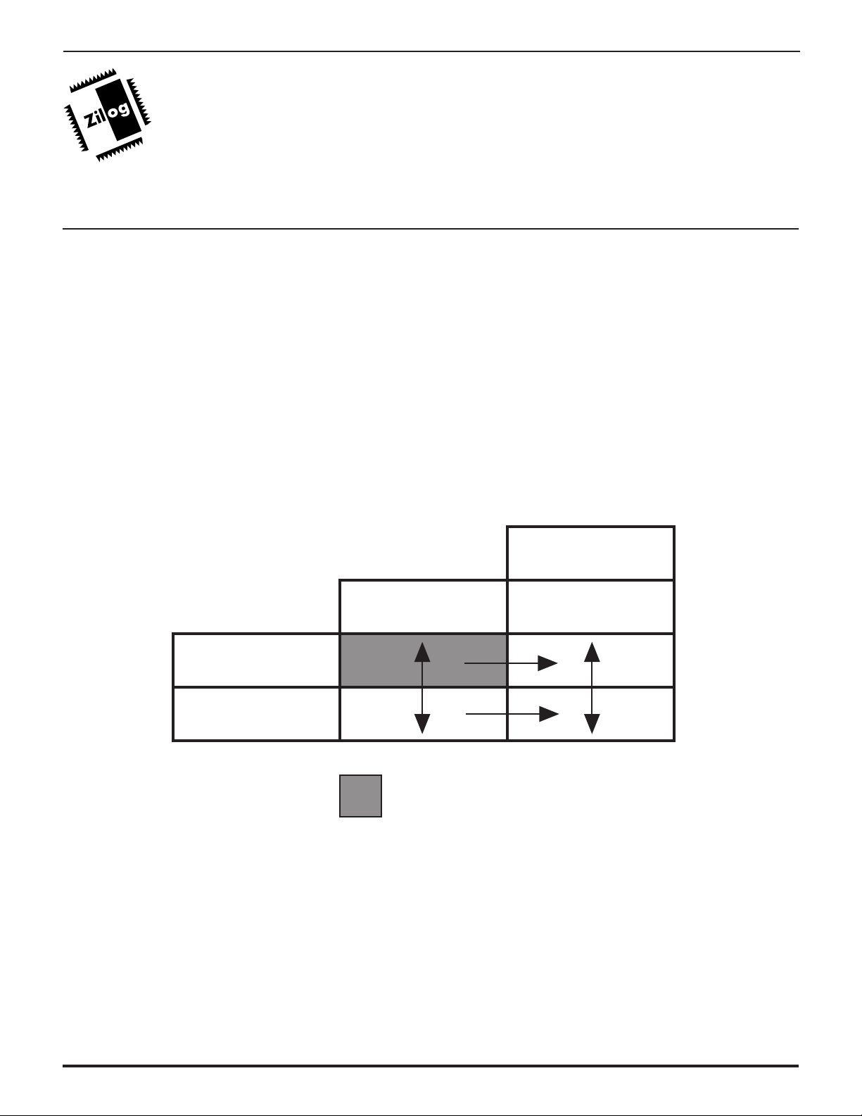
3.1 INTRODUCTION
U
SER
’s M
ANUAL
CHAPTER 3
NATIVE EXTENDED MODE, WORD/LONG
WORD MODE OF OPERATIONS
AND
DECODER DIRECTIONS
The Z380
™
CPU architecture allows access to 4 Gbytes
(2
32
) of memory addressing space, and 4G locations of
I/O. It offers 16/32-bit manipulation capability while main-
taining object-code compatibility with the Z80 CPU. In
order to implement these capabilities and new instruction
sets, it has two modes of operation for address manipula-
tion (Native or Extended mode), two modes of operation for
data manipulation (Word or Long Word mode), and a
special set of new Decoder Directives.
On Reset, the Z380 CPU defaults in Native mode and Word
mode. In this condition, it behaves exactly the same as the
Z80 CPU, even though it has access to the entire 4 Gbytes
of memory for data access and 4G locations of I/O space,
access to the newly added registers which includes Ex-
tended registers and register banks, and the capability of
executing all the Z380 instructions.
As described below, the Z380 CPU can be switched
between Word mode and Long Word mode during opera-
tion through the SETC LW and RESC LW instructions, or
Decoder Directives. The Native and Extended modes are
a key exception— it defaults up in Native mode, and can
be set to Extended mode by the instruction. Only Reset can
return it to Native mode. Figure 3-1 illustrates the relation-
ship between these modes of operation.
For the instructions which work with the DDIR instructions, refer to Appendix D and E.
Word
Long Word
Native
Z380
Extended
Z80 Native Mode
Figure 3-1. Z380
™
CPU Operation Modes

3-2
Z380
™
USER'S MANUAL
DC-8297-03
ZILOG
3.2 DECODER DIRECTIVES
The Decoder Directive is not an instruction, but rather a
directive to the instruction decoder. The instruction de-
coder may be directed to fetch an additional byte or word
of immediate data or address with the instruction, as well
as tagging the instruction for execution in either Word or
Long Word mode. Since the Z80 CPU architecture’s ad-
dressing convention in the memory is “least significant
byte first, followed by more significant bytes,” it is possible
to have such instructions to direct the instruction decoder
to fetch additional byte(s) of address information or imme-
diate data to extend the instruction.
All eight combinations of the two options are supported, as
shown below. Instructions which do not support decoder
directives are assembled by the instruction decoder as if
the decoder directive were not present.
■ DDIR W Word mode
■ DDIR IB,W Immediate byte, Word mode
■ DDIR IW,W Immediate Word, Word mode
■ DDIR IB Immediate byte
■ DDIR LW Long Word mode
■ DDIR IB,LW Immediate byte, Long Word mode
■ DDIR IW,LW Immediate Word, Long Word
mode
■ DDIR IW Immediate Word
The IB decoder directive causes the decoder to fetch an
additional byte immediately after the existing immediate
data or direct address, and in front of any trailing opcode
bytes (with instructions starting with DD-CB or FD-CB, for
example).
Likewise, the IW decoder directive causes the decoder to
fetch an additional word immediately after the existing
immediate data or direct address, and in front of any
trailing opcode bytes.
Byte ordering within the instruction follows the usual con-
vention; least significant byte first, followed by more signifi-
cant bytes. More-significant immediate data or direct
address bytes not specified in the instruction are read as
all zeros by the processor.
The W decoder directive causes the instruction decoder to
tag the instruction for execution in Word mode. This is
useful while the Long Word (LW) bit in the Select Register
(SR) is set, but 16-bit data manipulation is required for this
instruction.
The LW decoder directive causes the instruction decoder
to tag the instruction for execution in Long Word mode.
This is useful while the LW bit in the SR is cleared, but 32-
bit data manipulation is required for this instruction.
3.3 NATIVE MODE AND EXTENDED MODE
The Z380 CPU can operate in either Native or Extended
mode, as a way to manipulate addresses.
In Native mode (the Reset configuration), the Program
Counter only increments across 16 bits, and all stack Push
and Pop operations manipulate 16-bit quantities (two
bytes). Thus, Native mode is fully compatible with the Z80
CPU’s 64 Kbyte address space and programming model.
The extended portion of the Program Counter (PC31-
PC15) is forced to 0 and program address location next to
0000FFFFH is 00000000H in this mode. This means in
Native mode, program have to reside within the first 64
Kbytes of the memory addressing space.
In Extended mode, however, the PC increments across all
32 bits and all stack Push and Pop operations manipulate
32-bit quantities. Thus, Extended mode allows access to
the entire 4 Gbyte address space. In both Native and
Extended modes, the Z380 CPU drives all 32 bits of the
address onto the external address bus; only the PC incre-
ments and stack operations distinguish Native from Ex-
tended mode.
Note that regardless of Native or Extended mode, a 32-bit
address is always used for the data access. Thus, for data
reference, the complete 4 Gbytes of memory area may be
accessed. For example:
LD BC, (HL)
uses the 32-bit address value stored in HL31-HL0 (HLz
and HL) as a source location address. However, on Reset,
the HL31-HL16 portion (HLz) initializes to 00H. Unless HLz
is modified to other than 00H, operation of this instruction
is identical to the one with the Z80 CPU. Modifying the
extended portion of the register is done either by using a
32-bit load instruction (in Long Word mode, or with DDIR
LW instructions), or using a 16-bit load instruction with
SWAP instructions.

3-3
Z380
™
USER'S MANUAL
ZILOG
DC-8297-03
The Z380 CPU implements one instruction to switch to
Extended mode from Native mode; SETC XM (set Ex-
tended mode) places the Z380 CPU in Extended mode.
Once in Extended mode, only Reset can return it to Native
mode. On Reset, the Z380 is in Native mode. Refer to
Sections 4 and 5 for more examples.
3.4 WORD AND LONG WORD MODE OF OPERATION
The Z380 CPU can operate in either Word or Long Word
mode. In Word mode (the Reset configuration), all word
operations manipulate 16-bit quantities, and are compat-
ible with the Z80 CPU 16-bit operations. In the Long Word
mode, all word operations can manipulate 32-bit quanti-
ties. Note that the Native/Extended and Word/Long Word
selections are independent of one another, as Word/Long
Word pertains to data and operand address manipulation
only. The Z380 CPU implements two instructions and two
decoder directives to allow switching between these two
modes; SETC LW (Set Long Word) and RESC LW (Reset
Long Word) perform a global switch, while DDIR LW and
DDIR W are decoder directives that select a particular
mode only for the instruction that they precede.
Examples:
1. Effect of Word mode and Long Word mode
DDIR W
LD BC, (HL)
Loads BC15-BC0 from the location (HL) and
(HL+1), and BCz (BC31-BC16) remains un-
changed.
DDIR LW
LD BC, (HL)
Loads BC31-BC0 from the locations (HL) to (HL+3).
2. Immediate data load with DDIR instructions
DDIR IW,LW
LD HL,12345678H
Loads 12345678H into HL31-HL0.
DDIR IB,LW
LD HL,123456H
Loads 00123456H into HL31-HL0.
00H is appended as the Most significant byte as
HL31-HL24.
DDIR LW
LD HL,1234H
Loads 00001234H into HL31-HL0.
0000H is appended as the HL31-HL16 portion.
Zilog’s products are not authorized for use as critical compo-
nents in life support devices or systems unless a specific written
agreement pertaining to such intended use is executed between
the customer and Zilog prior to use. Life support devices or
systems are those which are intended for surgical implantation
into the body, or which sustains life whose failure to perform,
when properly used in accordance with instructions for use
provided in the labeling, can be reasonably expected to result in
significant injury to the user.
Zilog, Inc. 210 East Hacienda Ave.
Campbell, CA 95008-6600
Telephone (408) 370-8000
Telex 910-338-7621
FAX 408 370-8056
Internet: http://www.zilog.com
© 1994, 1995, 1996, 1997 by Zilog, Inc. All rights reserved. No
part of this document may be copied or reproduced in any form
or by any means without the prior written consent of Zilog, Inc.
The information in this document is subject to change without
notice. Devices sold by Zilog, Inc. are covered by warranty and
patent indemnification provisions appearing in Zilog, Inc. Terms
and Conditions of Sale only.
ZILOG, INC. MAKES NO WARRANTY, EXPRESS, STATUTORY,
IMPLIED OR BY DESCRIPTION, REGARDING THE INFORMA-
TION SET FORTH HEREIN OR REGARDING THE FREEDOM OF
THE DESCRIBED DEVICES FROM INTELLECTUAL PROPERTY
INFRINGEMENT. ZILOG, INC. MAKES NO WARRANTY OF MER-
CHANTABILITY OR FITNESS FOR ANY PURPOSE.
Zilog, Inc. shall not be responsible for any errors that may appear
in this document. Zilog, Inc. makes no commitment to update or
keep current the information contained in this document.

4-1
Z380
™
USER'S MANUAL
ZILOG
DC-8297-03
4.1 INSTRUCTION
U
SER
’s M
ANUAL
CHAPTER 4
ADDRESSING MODES AND DATA TYPES
An instruction is a consecutive list of one or more bytes in
memory. Most instructions act upon some data; the term
operand refers to the data to be operated upon. For Z380
™
CPU instructions, operands can reside in CPU registers,
memory locations, or I/O ports (internal or external). The
method used to designate the location of the operands for
an instruction are called addressing modes. The Z380
CPU supports seven addressing modes; Register, Imme-
diate, Indirect Register, Direct Address, Indexed, Program
Counter Relative Address, and Stack Pointer Relative. A
wide variety of data types can be accessed using these
addressing modes.
4.2 ADDRESSING MODE DESCRIPTIONS
The following pages contain descriptions of the address-
ing modes for the Z380 CPU. Each description explains
how the operand’s location is calculated, indicates which
address spaces can be accessed with that particular
addressing mode, and gives an example of an instruction
using that mode, illustrating the assembly language format
for the addressing modes.
4.2.1 Register (R, RX)
When this addressing mode is used, the instruction pro-
cesses data taken from one of the 8-bit registers A, B, C,
D, E, H, L, IXU, IXL, IYU, IYL, one of the 16-bit registers BC,
DE, HL, IX, IY, SP, or one of the special byte registers I or
R.
Storing data in a register allows shorter instructions and
faster execution that occur with instructions that access
memory.
Instruction
OPERATION REGISTER → OPERAND
The operand value is the contents of the register.
The operand is always in the register address space. The
register length (byte or word) is specified by the instruction
opcode. In the case of Long Word register operation, it is
specified either through the SETC LW instruction or the
DDIR LW decoder directive.
Example of R mode:
1. Load register in Word mode.
DDIR W ;Next instruction in Word mode
LD BC,HL ;Load the contents of HL into BC
BCz BC HLz HL
Before instruction
execution 1234 5678 9ABC DEF0
After instruction
execution 1234 DEF0 9ABC DEF0
2. Load register in Long Word mode.
DDIR LW ;Next instruction in Long Word mode
LD BC,HL ;Load the contents of HL into BC
BCz BC HLz HL
Before instruction
execution 1234 5678 9ABC DEF0
After instruction
execution 9ABC DEF0 9ABC DEF0
4.2.2 Immediate (IM)
When the Immediate addressing mode is used, the data
processed is in the instruction.
The Immediate addressing mode is the only mode that
does not indicate a register or memory address as the
source operand.

4-2
Z380
™
USER'S MANUAL
DC-8297-03
ZILOG
4.2.2 Immediate (IM) (Continued)
Instruction
OPERATION
OPERAND
The operand value is in the instruction
Immediate mode is often used to initialize registers. Also,
this addressing mode is affected by the DDIR Immediate
Data Directives to expand the immediate value to 24 bits
or 32 bits.
Example of IM mode:
1. Load immediate value into accumulator
LD A,55H ;Load hex 55 into the accumulator.
A
Before instruction execution 12
After instruction execution 55
4.2.3 Indirect Register (IR)
In Indirect Register addressing mode, the register speci-
fied in the instruction holds the address of the operand.
The data to be processed is in the location specified by the
BC, DE, or HL register (depending on the instruction) for
memory accesses, or C register for I/O.
Memory or
Instruction Register I/O Port
OPERATION REGISTER → Address → OPERAND
The operand value is the contents of the location whose address is in the register.
Depending on the instruction, the operand specified by IR
mode is located in either the I/O address space (I/O
instruction) or memory address space (all other instruc-
tions).
Indirect Register mode can save space and reduce ex-
ecution time when consecutive locations are referenced or
one location is repeatedly accessed. This mode can also
be used to simulate more complex addressing modes,
since addresses can be computed before data is ac-
cessed.
The address in this mode is always treated as a 32-bit
mode. After reset, the contents of the extend registers
(registers with “z” suffix) are initialized as 0's; hence, these
instructions will be executed just as for the Z80/Z180.
Example of IR mode:
1. Load accumulator from the contents of memory
pointed by (HL)
LD A, (HL) ;Load the accumulator with the data
;addressed by the contents of HL
A HLz,HL
Before instruction
execution 0F 12345678
After instruction
execution 0B 12345678
Memory location 12345678 0B
2. Load 24-bit immediate value into HL
register
DDIR IB, LW ;next instruction is in Long Word
mode, with ;an additional
immediate data
LD HL, 123456H ;load HLz, and HL with constant
123456H
This case, the Z380 CPU appends 00H as a MSB byte.
HLz HL
Before instruction execution 0987 6543
After instruction execution 0012 3456

4-3
Z380
™
USER'S MANUAL
ZILOG
DC-8297-03
4.2.4 Direct Address (DA)
When Direct Address mode is used, the data processed is
at the location whose memory or I/O port address is in the
instruction.
Instruction Memory or
OPERATION I/O Port
ADDRESS → OPERAND
The operand value is the contents of the location whose
address is in the instruction.
Depending on the instruction, the operand specified by
DA mode is either in the I/O address space (I/O instruction)
or memory address space (all other instructions).
This mode is also used by Jump and Call instructions to
specify the address of the next instruction to be executed.
(The address serves as an immediate value that is loaded
into the program counter.)
Also, DDIR Immediate Data Directives are used to expand
the direct address to 24 or 32 bits. Operand width is
affected by LW bit status for the load and exchange
instructions.
Example of DA mode:
1. Load BC register from memory location 00005E22H in Word mode
LD BC, (5E22H) ;Load BC with the data in address
;00005E22H
BC
Before instruction execution 1234
After instruction execution 0301
Memory location 00005E22 01
00005E23 03
2. Load BC register from memory location 12345E22H in Word mode
DDIR IW ;extend direct address by one word
LD BC, (12345E22H) ;Load BC with the data in address
;12345E22H
BC
Before instruction execution 1234
After instruction execution 0301
Memory location 12345E22 01
12345E23 03
3. Load BC register from memory location 12345E22H in Long Word mode
DDIR IW,LW ;extend direct address by one word,
;and operation in Long Word
LD BC, (12345E22H) ;Load BC with the data in address
;12345E22H
BCz BC
Before instruction execution 1234 5678
After instruction execution 0705 0301
Memory location 12345E22 01
12345E23 03
12345E24 05
12345E25 07

4-4
Z380
™
USER'S MANUAL
DC-8297-03
ZILOG
4.2.5 Indexed (X)
When the Indexed addressing mode is used, the data
processed is at the location whose address is the contents
of IX or IY in use, offset by an 8-bit signed displacement in
the instruction.
The Indexed address is computed by adding the 8-bit
two’s complement signed displacement specified in the
instruction to the contents of the IX or IY register in use, also
specified by the instruction. Indexed addressing allows
random access to tables or other complex data structures
where the address of the base of the table is known, but the
particular element index must be computed by the pro-
gram.
The offset portion can be expanded to 16 or 24 bits,
instead of eight bits by using DDIR Immediate Data Direc-
tives (DDIR IB for 16-bit offset, DDIR IW for 24-bit offset).
Note that computation of the effective address is affected
by the operation mode (Native or Extended). In Native
mode, address computation is done in modulo 2
16
, and in
Extended mode, address computation is done in modulo
2
32
.
Address calculation: In Native mode, 0FFH encoding in
the instruction is sign extended to a 16-bit value before the
address calculation, but calculation is done in modulo 2
16
and does not take into account the index register’s
extended portion.
0000
+ FFFF
FFFF
Instruction REGISTER MEMORY
OPERATION REGISTER → ADDRESS →+ OPERAND
DISPLACEMENT _____________________________________ ↑
Example of X mode:
1. Load accumulator from location (IX-1) in Native mode
LD A, (IX-1) ;Load into the accumulator the
;contents of the memory location
;whose address is one less than
;the contents of IX
;Assume it is in Native mode
A IXz IX
Before instruction execution 01 0001 0000
After instruction execution 23 0001 0000
Memory location 0001FFFF 23

4-5
Z380
™
USER'S MANUAL
ZILOG
DC-8297-03
2. Load accumulator from location (IX-1) in Extended mode
SETC XM ;Set Extended mode
LD A, (IX-1) ;Load into the accumulator the
;contents of the memory location
;whose address is one less than
;the contents of IX
A IXz IX
Before instruction execution 01 0001 0000
After instruction execution 23 0001 0000
Memory location 0000FFFF 23
Address calculation: In Extended mode, 0FFH encoding in
the instruction is sign extended to a 32-bit value before the
address calculation, but calculation is done in modulo 2
32
and takes into account the index register’s extended
portion.
00010000
+ FFFFFFFF
0000FFFF
4.2.6 Program Counter Relative Mode (RA)
The Program Counter Relative Addressing mode is used
by certain program control instructions to specify the
address of the next instruction to be executed (specifically,
the sum of the Program Counter value and the displace-
ment value is loaded into the Program Counter). Relative
addressing allows reference forward or backward from the
current Program Counter value; it is used for program
control instructions such as Jumps and Calls that access
constants in the memory.
As a displacement, an 8-bit, 16-bit, or 24-bit value can be
used. The address to be loaded into the Program Counter
is computed by adding the two’s complement signed
displacement specified in the instruction to the current
Program Counter.
Note that computation of the effective address is affected
by the mode of operation (Native or Extended). In Native
mode, address computation is done in modulo 2
16
, and the
PC Extend (PC31-PC16) is forced to 0 and will not affect
this portion. In Extended mode, address computation is
done is modulo 2
32
, and will affect the contents of PC
extend if there is a carry or borrow operation.
Also, in Native mode,
Instruction PC MEMORY
OPERATION ADDRESS →+ OPERAND
DISPLACEMENT —↑
Example of RA mode:
1. Jump relative in Native mode, 8-bit displacement
JR $-2 ;Jumps to the location
;(Current PC value) – 2
;’$’ represents for current PC value
;This instruction jumps to itself.
;since after the execution of this instruction,
;PC points to the next instruction.
 Loading...