


ZILOG Z8932320FEC, Z8932320FSC, Z8932320VEC, Z893232YFSC, Z8932320VSC Datasheet
...
|
P R E L I M I N A R Y |
Z89323/373/393 |
|
|
16-BIT DIGITAL SIGNAL PROCESSORS |
||
|
|
|
|
PRELIMINARY
CUSTOMERPROCUREMENTSPECIFICATION
Z89323/373/393
16-BITDIGITAL SIGNALPROCESSORS
FEATURES
|
DSP ROM |
OTP |
DSP RAM |
Max Core |
Device |
(K Words) |
(K Words) |
(Words) |
MIPS |
|
|
|
|
|
Z89323 |
8 |
|
512 |
2 0 |
Z89373 |
|
8 |
512 |
1 6 |
Z89393 |
64* |
|
512 |
2 0 |
Package |
44-Pin |
68-Pin 44-Pin 80-Pin 100-Pin |
||
Device |
PLCC |
PLCC |
QFP |
QFP QFP |
|
|
|
|
|
Z89323 |
|
|
|
|
Z89373 |
|
|
|
|
Z89393 |
|
|
|
|
* External |
|
|
|
|
|
|
|
■ |
Operating Temperature Ranges: |
On-Board Peripherals |
|||||
|
|
0°C to +70°C (Standard) |
|
|
|
||
|
–40°C to +85°C (Extended) |
|
■ |
4-Channel, 8-Bit Analog to Digital Converter (A/D) |
|||
■ 4.5- to 5.5-Volt Operating Range |
■ |
On-Board Serial Peripheral Interface (SPI) |
|||||
DSP Core |
|
|
|
■ |
Up to 40 Bits of Programmable I/O |
||
■ 20 MIPS @ 20 MHz, 16-Bit Fixed Point DSP |
■ |
Two Channels of Programmable |
|||||
|
|
|
|
|
|
|
Pulse Width Modulators (PWM) |
■ |
50 ns Instruction Cycle Time |
|
|
|
|||
|
|
|
|
|
|
■ Three General-Purpose Timer/Counters |
|
■ |
Single-Cycle Multiply and ALU Operations |
|
|
||||
|
|
|
|
|
|
■ Two Watch-Dog Timers (WDT) |
|
■ |
Two |
Internal |
Data Buses and |
Address Generators |
|
|
|
|
|
|
|
|
|
■ |
Programmable PLL |
■ |
Six |
Register |
Address |
Pointers |
|
|
|
|
|
|
|
|
|
■ Three Vectored Interrupts Servicing Eight |
|
■ |
Optimized Instruction |
Set (30 |
Instructions) |
|
Interrupt Sources |
||
|
|
|
|
|
|
■ |
Power-Down and Power-On Reset |
GENERAL DESCRIPTION
The Z89323/373/393 DSP family of products builds on Zilog's first generation Z893XX DSP core, integrating several peripherals especially well suited for cost-effective voice, telephony, and control applications.
These DSP devices feature a modified Harvard architecture supported by one program bus and two on-chip data buses. This bus structure is supported by two address generators and six register pointers to ensure that the 20 MIPS DSP CPU is continually active.
The Z893X3 DSP family is designed to provide a complete DSP and control system on a single chip. By integrating
various peripherals, such as a high-speed 4-channel, 8-bit A/D, an SPI, three timers with PWM and WDT support, the Z893X3 family provides a compact system solution and reduces overall system cost.
To support a wide variety of development needs, the Z893X3 DSP product family features the cost-effective Z89323 with 8 Kwords of on-chip ROM, and the Z89373, a 16-MIPS OTP version of the Z89323, ideal for prototypes and early production builds. For systems requiring more than 8 Kwords of program memory, the Z89393 device can address up to 64 Kwords of external program memory.
DS95DSP0101 Q4/95 |
1 |
P R E L I M I N A R Y |
Z89323/373/393 |
16-BIT DIGITAL SIGNAL PROCESSORS |
GENERAL DESCRIPTION (Continued)
The Z893X3 DSP family is 100 percent source and objectcode compatible with the existing Z89321/371/391 devices, providing users, who can benefit from increased integration and reduced system cost, an easy migration path from one DSP product to the next.
Notes:
All Signals with a preceding front slash, "/", are active Low, e.g., B//W (WORD is active Low); /B/W (BYTE is active Low, only).
Power connections follow conventional descriptions below:
Connection Circuit Device
Throughout this specification, references to the Z89323 |
|
|
|
|
|
|
|
|
|
|
|
|
|
|
|
|
|
|
|
|
|
|
|
|
|
|
|
||||||||||||||||||||||||||||||||||||||||
|
|
|
Power |
|
|
|
|
|
VCC |
|
|
|
|
|
|
VDD |
|||||||||||||||||||||||||||||||||||||||||||||||||||
device applies equally to the Z89373 and Z89393, unless |
|
|
|
|
|
|
|
|
|
|
|
|
|
||||||||||||||||||||||||||||||||||||||||||||||||||||||
otherwise |
specified. |
|
|
|
|
|
|
|
|
|
|
|
|
|
|
|
|
|
|
|
|
|
|
|
|
|
|
|
|
|
|
|
|
Ground |
|
|
|
|
|
GND |
|
|
|
|
|
|
VSS |
||||||||||||||||||||
|
|
|
|
|
|
|
|
|
|
|
|
|
|
|
|
|
|
|
|
|
|
|
|
|
|
|
|
|
|
|
|
|
|
|
|
|
|
|
|
|
|
|
|
|
|
|
|
|
|
|
|
|
|
|
|
|
|
|
|
|
|
|
|
|
|
|
|
|
|
|
|
|
|
|
|
|
|
|
|
|
|
|
|
|
|
|
|
|
|
|
Program |
|
Data RAM0 |
|
|
|
|
|
|
|
Data RAM1 |
|
|
|
|
|
|
|
|
|
|
|
|
|
|
|
|
|
|
||||||||||||||||
|
|
|
|
|
|
|
|
|
|
|
|
|
|
|
|
|
|
|
|
|
ROM/OTP |
|
|
|
|
|
|
|
|
|
|
|
|
|
|
|
|
|
|
|
|
|
|
|
|
Port 0 |
|||||||||||||||||||||
PD0-15 |
|
|
|
|
|
|
|
|
|
|
|
|
|
|
|
|
|
|
|
8192x16 |
|
|
256x16 |
|
|
|
|
|
|
256x16 |
|
|
16-Bit |
|
|
|
|
|
|
|
|
|
|
|
/EXTEN |
||||||||||||||||||||||
|
|
|
|
|
|
|
|
|
|
|
|
|
|
|
|
|
|
|
|
|
|
|
|
|
|
|
|
|
|
|
|
|
|
|
|
|
|
|
|
|
|
|
|
|
|
|
|||||||||||||||||||||
|
|
|
|
|
|
|
|
|
|
|
|
|
|
|
|
|
|
|
|
|
|
|
|
|
|
|
|
|
|
|
|
|
|
|
|
|
|
|
|
|
|
|
|
|
|
|
|
|
|
|
|
Program |
|
|
|
|
|
|
|
|
|
|
|
||||
PA0-15 |
|
|
|
|
|
|
PDATA |
|
|
|
|
|
|
|
|
|
|
|
|
|
|
|
|
|
|
|
|
|
|
|
|
|
|
|
|
|
|
|
|
|
|
|
|
|
|
|
|
|
I/O |
|
|
|
|
|
|
|
|
|
|
|
EA0-2 |
||||||
|
|
|
|
|
|
|
|
|
|
|
|
|
|
|
|
|
|
|
|
|
|
|
|
|
|
|
|
|
|
|
|
|
|
|
|
|
|
|
|
|
|
|
|
|
|
|
|
|
|
|
|
|
|
|
|
|
|
|
|
|
|
|
EXT0-15/P00-15 |
||||
|
|
|
|
|
|
|
|
|
PADDR |
|
|
|
|
|
|
|
|
|
|
|
|
|
|
|
|
|
|
|
DDATA |
|
|
|
|
|
|
|
|
|
|
|
|
|
|
|
|
|
|
|
|
|
|
|
|
|
|
|
|
|
|
|
|
|
/DS |
||||
|
|
|
/PAZ |
|
|
|
|
|
|
|
|
|
|
|
|
|
|
|
|
|
|
|
|
|
|
|
|
|
|
|
|
|
|
|
|
|
|
|
|
|
|
|
|
|
|
|
|
|
|
|
|
|
|
|
|
|
|
|
|
|
|||||||
|
|
|
|
|
|
|
|
|
|
|
|
|
|
|
|
|
|
|
|
|
|
|
|
|
|
|
|
|
|
|
|
|
|
|
|
|
|
|
|
|
|
|
|
|
|
|
|
|
|
|
|
|
|
|
|
|
|
|
|
|
|
|
|
|
|
WAIT |
|
|
|
|
|
|
|
|
|
|
|
|
|
|
|
|
|
|
|
|
|
|
|
|
|
|
|
|
|
|
|
|
|
|
|
|
|
|
|
|
|
|
|
|
|
|
|
|
|
|
|
|
|
|
|
|
|
|
|
|
|
|
|
|
|
|
|
|
RD//WR |
|
|
|
|
|
|
|
|
|
|
|
|
|
|
|
|
|
|
|
|
|
|
|
|
|
|
|
|
|
|
|
XDATA |
|
|
|
|
|
|
|
|
|
|
|
|
|
|
|
|
|
|
|
|
|
|
|
|
|
|
|
|
|
|
|
|
|
|
||
|
|
|
|
|
|
|
|
|
|
|
|
|
|
|
|
|
|
|
|
|
|
|
|
|
|
|
|
|
|
|
|
|
|
|
|
|
|
|
P0 |
P0 |
|
|
|
|
|
|
|
|
|
|
|
|
|
|
|
|
|
|
|
|
AN0 |
||||||
|
|
|
|
|
|
|
|
|
|
|
|
|
|
|
|
|
|
|
|
|
|
|
|
|
|
|
|
|
|
|
|
|
|
|
|
|
|
|
P1 |
P1 |
|
|
|
|
|
|
|
|
|
|
|
|
|
|
|
|
|
|
|
|
|
||||||
|
|
|
|
|
|
|
|
|
|
|
|
|
|
|
|
|
|
|
|
|
|
|
|
|
|
|
|
|
|
|
|
|
|
|
|
|
|
|
|
|
|
|
|
|
|
|
8-Bit |
|
|
|
|
|
|
|
|
|
AN1 |
||||||||||
|
|
|
|
|
|
|
|
|
|
|
|
|
|
|
|
|
|
|
|
|
|
|
|
|
|
|
|
|
|
|
|
|
|
|
|
|
|
|
|
|
|
|
|
|
|
|
|
|
|
|
|
|
|
|
|||||||||||||
|
|
|
|
|
|
|
|
|
|
|
|
|
|
|
|
|
|
|
X |
|
|
|
|
Y |
|
|
|
|
|
|
|
|
P2 |
P2 |
|
|
|
|
|
|
|
|
|
A/D |
|
|
|
|
|
|
|
|
|
|
AN2 |
||||||||||||
|
|
|
|
|
|
|
|
|
|
|
|
|
|
|
|
|
|
|
|
|
|
|
|
|
|
|
|
|
|
|
|
|
|
|
|
|
|
|
|
|
|
|
|
|
|
|
|
|
|
|
|
AN3 |
|||||||||||||||
|
|
|
|
|
|
|
|
|
|
|
|
|
|
|
|
|
|
|
Multiplier |
|
|
|
|
|
|
|
DP0-3 |
DP4-6 |
|
|
|
|
|
|
|
|
|
|
|
|
|
|
|
|
|
|
|
|
|
||||||||||||||||||
|
|
|
HALT |
|
|
|
|
|
|
|
|
|
|
|
|
|
|
|
|
|
|
|
|
|
|
|
|
|
|
|
|
|
|
|
|
|
|
|
|
|
|
|
|
|
|
|
Port 1 |
||||||||||||||||||||
|
|
|
|
|
|
|
|
|
|
|
|
|
|
|
|
|
|
|
|
|
|
|
|
|
|
|
|
|
|
|
|
|
|
|
|
|
|
|
|
|
|
|
|
|
|
|
|
|
|
|
|
|
|
|
|
|
|
|
|
|
|
|
|
|
|
||
/ROMEN |
|
|
|
|
|
|
|
|
|
|
|
|
|
|
|
|
|
|
|
|
P |
|
|
|
|
|
|
|
|
|
ADDR |
ADDR |
|
|
|
|
|
|
|
|
|
|
|
|
|
|
|
|
|
|
|
|
|
P10-17 |
|||||||||||||
|
|
|
|
|
|
|
|
|
|
|
|
|
|
|
|
|
|
|
|
|
|
|
|
|
|
|
|
|
|
|
|
|
|
|
GEN0 |
GEN1 |
|
|
|
|
|
|
|
|
|
|
|
|
|
|
|
|
|
|
|
|
|
or |
|||||||||
|
|
|
|
|
|
|
|
|
|
|
|
|
|
|
|
|
|
|
|
|
|
|
|
|
|
|
|
|
|
|
|
|
|
|
|
|
|
|
|
|
|
|
|
|
|
|
|
|
|
|
|
|
|
|
|
|
|
|
|
||||||||
|
|
|
/RES |
|
|
|
|
|
|
|
|
|
|
|
|
|
|
|
|
|
Shifter |
|
|
|
|
|
|
|
|
|
|
|
|
|
|
|
|
|
|
|
|
|
|
|
|
|
|
8-Bit I/O |
|
|
|
|
|
|
INT2 |
||||||||||||
|
|
|
CLKI |
|
|
|
|
|
|
|
|
|
|
|
|
|
|
|
|
|
|
|
|
|
|
|
|
|
|
|
|
|
|
|
|
|
|
|
|
|
|
|
|
|
|
|
|
|
|
|
|
|
|
|
|
|
|
|
|
|
CLKOUT |
||||||
|
|
|
|
|
|
|
|
|
|
|
|
|
|
|
|
|
|
|
|
|
|
|
|
|
|
|
|
|
|
|
|
|
|
|
|
|
|
|
|
|
|
|
|
|
|
|
|
|
|
|
|
|
|
|
|
|
|
|
|
|
|
|
|
|
|
SIN |
|
|
|
CLKO |
|
|
|
|
|
|
|
|
|
|
|
|
|
|
|
|
|
|
|
|
|
|
|
|
|
|
|
|
|
|
|
|
|
|
|
|
|
|
|
|
|
|
|
|
|
|
|
|
|
|
|
|
|
|
|
|
|
|
|
|
|
|
|
||
|
|
|
|
|
Program |
|
|
|
|
|
|
|
|
|
|
|
|
|
|
|
|
|
|
|
|
|
|
|
|
|
|
|
|
|
|
|
|
|
|
|
|
|
|
|
|
|
|
|
|
|
|
|
|
|
|
|
|
|
|
|
|
SOUT |
|||||
|
|
|
AGND |
|
|
|
|
|
|
|
|
Arithmetic |
|
|
|
|
|
|
|
|
|
|
|
|
|
|
|
|
|
|
|
|
|
|
|
|
|
|
|
|
|
|
|
|
|
|
|
|
|
|
|
|
SK |
||||||||||||||
|
|
|
|
|
|
Control |
|
|
|
|
|
|
|
|
|
|
|
|
|
|
|
|
|
|
|
|
|
|
|
|
|
|
|
|
|
|
|
|
|
|
|
|
|
|
|
|
|
|
|
|
|
||||||||||||||||
|
|
|
|
|
|
|
|
|
|
|
Logic Unit |
|
|
|
|
|
|
|
|
|
|
|
|
|
|
|
|
|
|
|
|
|
|
|
|
|
|
|
|
|
|
|
|
|
|
|
|
|
|
|
|
||||||||||||||||
|
|
|
|
|
|
|
|
Unit |
|
|
|
|
|
|
|
|
|
|
|
|
|
|
|
|
|
|
|
|
|
|
|
|
|
|
|
|
|
|
|
|
|
|
|
|
|
|
|
|
|
|
|
|
|
SS |
|||||||||||||
ANVCC |
|
|
|
|
|
|
|
|
|
|
(ALU) |
|
|
|
|
|
|
|
|
|
|
|
|
|
|
|
|
|
|
|
|
|
|
|
|
|
|
|
|
|
|
|
|
|
|
|
|
|
|
|
|
||||||||||||||||
|
|
|
|
|
|
|
|
|
|
|
|
|
|
|
|
|
|
|
|
|
|
|
|
|
|
|
|
|
|
|
|
|
|
|
|
|
|
|
|
|
|
|
|
|
|
|
|
|
|
|
|
|
UI0-1 |
||||||||||||||
|
|
|
VALO |
|
|
|
|
|
|
|
|
|
|
|
|
|
|
|
|
|
|
|
|
|
|
|
|
|
|
|
|
|
|
|
|
|
|
|
|
|
|
|
|
16-Bit Timer, |
|
|
|
|
|
|
|
|
|
|
|
|
|
|
|
|
|
|
|
||||
|
|
|
|
|
|
|
|
|
|
|
|
|
|
|
|
|
|
|
|
|
|
|
|
|
|
|
|
|
|
|
|
|
|
|
|
|
|
|
|
|
|
|
|
|
|
|
|
|
|
|
|
|
|
|
|
|
|
|
|
|
|
||||||
|
|
|
|
|
|
|
|
|
|
|
|
|
|
|
|
|
|
|
|
|
|
|
|
|
|
|
|
|
|
|
|
|
|
|
|
|
|
|
|
|
|
|
|
Counter |
|
|
|
|
|
|
|
|
|
|
|
|
|
|
|
|
|
|
|
Port 2 |
|||
|
|
|
|
|
|
|
|
|
|
|
|
|
|
|
|
|
|
|
|
|
|
|
|
|
|
|
|
|
|
|
|
|
|
|
|
|
|
|
|
|
|
|
|
|
|
|
|
|
|
|
|
|
|
|
|
|
|
|
|
|
|
|
|||||
|
|
|
VALI |
|
|
|
|
|
|
|
|
|
|
|
|
Accumulator |
|
|
|
|
|
|
|
|
|
|
|
|
|
|
|
|
|
|
|
|
|
|
|
|
|
|
|
|
|
|
|
|
|
|
|
|
|
|
|
P20-27 |
|||||||||||
|
|
|
VSS |
|
|
|
|
|
|
|
|
|
|
|
|
|
|
|
|
|
|
|
|
|
|
|
|
|
|
|
|
|
|
|
|
|
|
|
|
|
|
|
|
16-Bit Timer, |
|
|
|
|
|
|
|
|
|
|
|
|
|
|
|
|
|
|
or |
||||
|
|
|
|
|
|
|
|
|
|
|
|
|
|
|
|
|
|
|
|
|
|
|
|
|
|
|
|
|
|
|
|
|
|
|
|
|
|
|
|
|
|
|
Counter, PWM |
|
|
|
|
|
|
|
|
|
|
|
|
|
|
|
|
|
|
|
|||||
|
|
|
VDD |
|
|
|
|
|
|
|
|
|
|
|
|
|
|
|
|
|
|
|
|
|
|
|
|
|
|
|
|
|
|
|
|
|
|
|
|
|
|
|
|
|
|
|
|
|
|
8-Bit I/O |
|
|
|
|
|
|
UI2 |
||||||||||
|
|
|
|
|
|
|
|
|
|
|
|
|
|
|
|
|
|
|
|
|
|
|
|
|
|
|
|
|
|
|
|
|
|
|
|
|
|
|
|
|
|
|
|
|
|
|
|
|
|
|
|
|
|
|
|
|
|
|
|
||||||||
|
|
|
|
|
|
|
|
|
|
|
|
|
|
|
|
|
|
|
|
|
|
|
|
|
|
|
|
|
|
|
|
|
|
|
|
|
|
|
|
|
|
|
|
|
|
|
|
|
|
|
|
|
|
|
|
|
|
|
|
||||||||
|
|
|
|
|
|
|
|
|
|
|
|
|
|
|
|
|
|
|
|
|
|
|
|
|
|
|
|
|
|
|
|
|
|
|
|
|
|
|
|
|
|
|
|
|
|
|
|
|
|
|
|
|
|
|
|
|
|
|
|
||||||||
|
|
|
|
|
|
|
|
|
|
|
|
|
|
|
|
|
|
|
|
|
|
|
|
|
|
|
|
|
|
|
|
|
|
|
|
|
|
|
|
|
|
|
|
16-Bit Timer, |
|
|
|
|
|
|
|
|
|
|
|
|
|
|
|
|
|
|
UO0-2 |
||||
|
|
|
|
|
|
|
|
|
|
|
|
|
|
|
|
|
|
|
|
|
|
|
|
|
|
|
|
|
|
|
|
|
|
|
|
|
|
|
|
|
|
|
|
Counter, PWM |
|
|
|
|
|
|
|
|
|
|
|
|
|
|
|
|
|
|
|
||||
|
|
|
|
|
|
|
|
|
|
|
|
|
|
|
|
|
|
|
|
|
|
|
|
|
|
|
|
|
|
|
|
|
|
|
|
|
|
|
|
|
|
|
|
|
|
|
|
|
|
|
|
|
|
|
|
|
|
|
|
|
|
|
|||||
|
|
|
|
|
|
|
|
|
|
|
|
|
|
|
|
|
|
|
|
|
|
|
|
|
|
|
|
|
|
|
|
|
|
|
|
|
|
|
|
|
|
|
|
|
|
|
|
|
|
|
|
|
|
|
|
|
|
|
|
|
|
|
|
|
|
|
INT0-1 |
|
|
|
|
|
|
|
|
|
|
|
|
|
|
|
|
|
|
|
|
|
|
|
|
|
|
|
|
|
|
|
|
|
|
|
|
|
|
|
|
|
|
|
|
|
|
|
|
|
|
|
|
|
|
|
|
|
|
|
|
|
|
|
|
|
|
|
|
|
|
|
|
|
|
|
|
|
|
|
|
|
|
|
|
|
|
|
|
|
|
|
|
|
|
|
|
|
|
|
|
|
|
|
|
|
|
|
|
|
|
|
|
|
|
SPI |
|
|
|
|
|
|
|
|
|
|
|
|
|
|
|
|
|
|
|
||
|
|
|
|
|
|
|
|
|
|
|
|
|
|
|
|
|
|
|
|
|
|
|
|
|
|
|
|
|
|
|
|
|
|
|
|
|
|
|
|
|
|
|
|
|
|
|
|
|
|
|
|
|
|
|
|
|
|
|
|
|
|
|
|
|
Port 3 |
||
|
|
|
|
|
|
|
|
|
|
|
|
|
|
|
|
|
|
|
|
|
|
|
|
|
|
|
|
|
|
|
|
|
|
|
|
|
|
|
|
|
|
|
|
|
|
|
|
|
|
|
|
|
|
|
|
|
|
|
|
|
|
|
|
||||
|
|
|
|
|
|
|
|
|
|
|
|
|
|
|
|
|
|
|
|
|
|
|
|
|
|
|
|
|
|
|
|
|
|
|
|
|
|
|
|
|
|
|
|
|
|
|
|
|
|
|
|
|
|
|
|
|
|
|
|
|
|
|
|
|
|||
|
|
|
|
|
|
|
|
|
|
|
|
|
|
|
|
|
|
|
|
|
|
|
|
|
|
|
|
|
|
|
|
|
|
|
|
|
|
|
|
|
|
|
|
|
|
|
|
|
|
|
|
|
|
|
|
|
|
|
|
|
|
|
|
|
|
|
|
|
|
|
|
|
|
|
|
|
|
|
|
|
|
|
|
|
|
|
|
|
|
|
|
|
|
|
|
|
|
|
|
|
|
|
|
|
|
|
|
|
|
|
|
|
|
|
|
|
|
|
|
|
|
|
4 Inputs |
|
|
|
|
|
|
||||||
|
|
|
|
|
|
|
|
|
|
|
|
|
|
|
|
|
|
|
|
|
|
|
|
|
|
|
|
|
|
|
|
|
|
|
|
|
|
|
|
|
|
|
|
|
|
|
|
|
|
|
|
|
|
|
|
|
|
|
|
|
P30-33 |
||||||
|
|
|
|
|
|
|
|
|
|
|
|
|
|
|
|
|
|
|
|
|
|
|
|
|
|
|
|
|
|
|
|
|
|
|
|
|
|
|
|
|
|
|
|
|
|
|
|
|
|
|
|
|
|
|
|
|
|
|
|
|
|||||||
|
|
|
|
|
|
|
|
|
|
|
|
|
|
|
|
|
|
|
|
|
|
|
|
|
|
|
|
|
|
|
|
|
|
|
|
|
|
|
|
|
|
|
|
|
|
|
|
|
|
|
|
|
|
|
4 Outputs |
|
|
|
|
|
|
P34-37 |
|||||
|
|
|
|
|
|
|
|
|
|
|
|
|
|
|
|
|
|
|
|
|
|
|
|
|
|
|
|
|
|
|
|
|
|
|
|
|
|
|
|
|
|
|
|
|
|
|
|
|
|
|
|
|
|
|
|
|
|
|
|
|
|||||||
|
|
|
|
|
|
|
|
|
|
|
|
|
|
|
|
|
|
|
|
|
|
|
|
|
|
|
|
|
|
|
|
|
|
|
|
|
|
|
|
|
|
|
|
|
|
|
|
|
|
|
|
|
|
|
|
|
|
|
|
|
|
|
|
|
|
|
|
Figure 1. Z893X3 Functional Block Diagram
2 |
DS95DSP0101 Q4/95 |
|
P R E L I M I N A R Y |
|
|
Z89323/373/393 |
||||||||||
|
|
|
16-BIT DIGITAL SIGNAL PROCESSORS |
|||||||||||
PIN DESCRIPTION |
|
|
|
|
|
|
|
|
|
|
|
|
|
|
|
EXT15/P015 |
VSS |
EXT14/P014 |
EXT13/P013 |
EXT12/P012 |
P20/INT0 |
VSS |
EXT2/P02 |
EXT1/P01 |
EXT0/P00 |
VSS |
|
||
|
6 |
5 |
4 |
3 |
2 |
1 |
44 |
43 |
42 |
41 |
40 |
|
||
EXT3/P03 |
7 |
|
|
|
|
|
|
|
|
|
|
|
39 |
/RES |
|
|
|
|
|
|
|
|
|
|
|
||||
EXT4/P04 |
8 |
|
|
|
|
|
|
|
|
|
|
|
38 |
WAIT |
VSS |
9 |
|
|
|
|
|
|
|
|
|
|
|
37 |
P24/UO2 |
EXT5/P05 |
10 |
|
|
|
|
|
|
|
|
|
|
|
36 |
P22/UO0 |
EXT6/P06 |
11 |
|
|
|
Z89323/373 |
|
|
|
35 |
CLKO |
||||
EXT7/P07 |
12 |
|
|
|
|
|
|
34 |
CLKI |
|||||
|
|
|
44-Pin PLCC |
|
|
|
||||||||
INT1/P21 |
13 |
|
|
|
|
|
|
33 |
/DS |
|||||
|
|
|
|
|
|
|
|
|
|
|
||||
EXT8/P08 |
14 |
|
|
|
|
|
|
|
|
|
|
|
32 |
P23/UO1 |
EXT9/P09 |
15 |
|
|
|
|
|
|
|
|
|
|
|
31 |
EA2 |
VSS |
16 |
|
|
|
|
|
|
|
|
|
|
|
30 |
EA1 |
EXT10/P010 |
17 |
|
|
|
|
|
|
|
|
|
|
|
29 |
EA0 |
|
18 |
19 |
20 |
21 |
22 |
23 |
24 |
25 |
26 |
27 |
28 |
|
||
|
1/P011 EXT1 |
AHIV |
ALOV |
ANGND |
AN0 |
AN1 |
AN2 |
AN3 |
ANVCC |
VDD |
|
RD//WR |
|
|
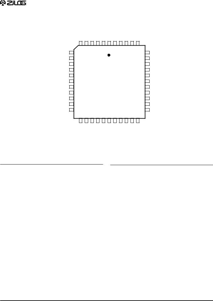
Figure 2. 44-Pin PLCC Z89323/373 Pin Configuration
Table 1. 44-Pin PLCC Z89323/373 Pin Description
No. |
Symbol |
Function |
Direction |
|
|
|
|
1 |
P20/INT0 |
Port20/Interrupt0 |
In/Output |
2 |
EXT12/P012 |
ExtData12/Port012 |
In/Output |
3 |
EXT13/P013 |
ExtData13/Port013 |
In/Output |
4 |
EXT14/P014 |
ExtData14/Port014 |
In/Output |
5 |
VSS |
Ground |
|
6 |
EXT15/P015 |
ExtData15/Port015 |
In/Output |
7 |
EXT3/P03 |
ExtData3/Port03 |
In/Output |
8 |
EXT4/P04 |
ExtData4/Port04 |
In/Output |
9 |
VSS |
Ground |
In/Output |
10 |
EXT5/P05 |
ExtData5/Port05 |
|
|
|
|
|
11 |
EXT6/P06 |
ExtData6/Port06 |
In/Output |
12 |
EXT7/P07 |
ExtData7/Port07 |
In/Output |
13 |
P21/INT1 |
Port21/Interrupt1 |
In/Output |
14 |
EXT8/P08 |
ExtData8/Port08 |
In/Output |
15 |
EXT9/P09 |
ExtData9/Port09 |
In/Output |
|
|
|
|
16 |
VSS |
Ground |
In/Output |
17 |
EXT10/P010 |
ExtData10/Port010 |
|
18 |
EXT11/P011 |
ExtData11/Port011 |
In/Output |
19 |
VAHI |
AnalogHighRef. |
Input |
20 |
VALO |
AnalogLowRef. |
Input |
21 |
ANGND |
AnalogGround |
Input |
22 |
AN0 |
A/DInput0 |
Input |
|
|
|
|
No. |
Symbol |
Function |
Direction |
|
|
|
|
23 |
AN1 |
A/DInput1 |
Input |
24 |
AN2 |
A/DInput2 |
Input |
25 |
AN3 |
A/DInput3 |
Input |
26 |
ANVCC |
AnalogPower |
Input |
27 |
V |
Power |
|
|
DD |
|
|
|
|
|
|
28 |
RD//WR |
R/WExternalBus |
Output |
29 |
EA0 |
ExtAddress0 |
Output |
30 |
EA1 |
ExtAddress1 |
Output |
31 |
EA2 |
ExtAddress2 |
Output |
32 |
P23/UO1 |
Port23/UserOutput1 |
In/Output |
|
|
|
|
33 |
/DS |
ExtDataStrobe |
Output |
34 |
CLKI |
Clock/CrystalIn |
Input |
35 |
CLKO |
Clock/CrystalOut |
Input |
36 |
P22/UO0 |
Port22/UserOutput0 |
In/Output |
37 |
P24/UO2 |
Port24/UserOutput2 |
In/Output |
|
|
|
|
38 |
WAIT |
WaitforExt |
Input |
39 |
/RES |
Reset |
Input |
40 |
V |
Ground |
|
41 |
SS |
ExtData0/Port00 |
In/Output |
EXT0/P00 |
|||
42 |
EXT1/P01 |
ExtData1/Port01 |
In/Output |
43 |
EXT2/P02 |
ExtData2/Port02 |
In/Output |
44 |
V |
Ground |
|
|
SS |
|
|
DS95DSP0101 Q4/95 |
3 |
P R E L I M I N A R Y |
Z89323/373/393 |
16-BIT DIGITAL SIGNAL PROCESSORS |
PIN DESCRIPTION (Continued)
|
|
|
|
NC |
|
EXT15/P015 |
VSS |
EXT14/P014 |
VDD |
EXT13/P013 |
EXT12/P012 |
P20/INT0 |
P12/SIN |
P11/CLKOUT |
VSS |
P10 |
|
EXT2/P02 |
|
EXT1/P01 |
EXT0/P00 |
VSS |
|
VDD |
|||||||||||||||||
|
|
|
|
|
|
|
|
|
|
|
|
|
|
|
|
|
|
|
|
|
|
|
|
|
|
|
|
|
|
|
|
|
|
|
|
|
|
|
|
|
|
|
|
|
|
|
|
|
|
|
|
|
|
|
|
|
|
|
|
|
|
|
|
|
|
|
|
|
|
|
|
|
|
|
|
|
|
|
|
|
|
|
|
|
|
9 |
|
8 |
|
7 |
|
6 |
|
5 |
|
4 |
|
3 |
|
2 |
|
1 |
|
68 |
67 |
66 |
65 |
64 |
63 |
62 |
61 |
|
|||||||||||||
|
|
|
|||||||||||||||||||||||||||||||||||||||
NC |
|
10 |
|
|
|
|
|
|
|
|
|
|
|
|
|
|
|
|
|
|
|
|
|
|
|
|
|
|
|
|
|
|
|
|
|
|
60 |
||||
|
|
|
|
|
|
|
|
|
|
|
|
|
|
|
|
|
|
|
|
|
|
|
|
|
|
|
|
|
|
|
|
|
|
|
|||||||
|
|
|
|
|
|
|
|
|
|
|
|
|
|
|
|
|
|
|
|
|
|
|
|
|
|
|
|
|
|
|
|
||||||||||
|
11 |
|
|
|
|
|
|
|
|
|
|
|
|
|
|
|
|
|
|
|
|
|
|
|
|
|
|
|
|
|
|
|
|
|
|
59 |
|||||
EXT3/P03 |
|
|
|
|
|
|
|
|
|
|
|
|
|
|
|
|
|
|
|
|
|
|
|
|
|
|
|
|
|
|
|
|
|
|
|
||||||
EXT4/P04 |
|
12 |
|
|
|
|
|
|
|
|
|
|
|
|
|
|
|
|
|
|
|
|
|
|
|
|
|
|
|
|
|
|
|
|
|
|
58 |
||||
|
|
|
|
|
|
|
|
|
|
|
|
|
|
|
|
|
|
|
|
|
|
|
|
|
|
|
|
|
|
|
|
|
|
|
|||||||
VSS |
|
13 |
|
|
|
|
|
|
|
|
|
|
|
|
|
|
|
|
|
|
|
|
|
|
|
|
|
|
|
|
|
|
|
|
|
|
57 |
||||
|
|
|
|
|
|
|
|
|
|
|
|
|
|
|
|
|
|
|
|
|
|
|
|
|
|
|
|
|
|
|
|
|
|
|
|||||||
VDD |
|
14 |
|
|
|
|
|
|
|
|
|
|
|
|
|
|
|
|
|
|
|
|
|
|
|
|
|
|
|
|
|
|
|
|
|
|
56 |
||||
|
|
|
|
|
|
|
|
|
|
|
|
|
|
|
|
|
|
|
|
|
|
|
|
|
|
|
|
|
|
|
|
|
|
|
|||||||
EXT5/P05 |
|
15 |
|
|
|
|
|
|
|
|
|
|
|
|
|
|
|
|
|
|
|
|
|
|
|
|
|
|
|
|
|
|
|
|
|
|
55 |
||||
|
|
|
|
|
|
|
|
|
|
|
|
|
|
|
|
|
|
|
|
|
|
|
|
|
|
|
|
|
|
|
|
|
|
|
|||||||
|
16 |
|
|
|
|
|
|
|
|
|
|
|
|
|
|
|
|
|
|
|
|
|
|
|
|
|
|
|
|
|
|
|
|
|
|
54 |
|||||
SOUT/P13 |
|
|
|
|
|
|
|
|
|
|
|
|
|
|
|
|
|
|
|
|
|
|
|
|
|
|
|
|
|
|
|
|
|
|
|
||||||
EXT6/P06 |
|
17 |
|
|
|
|
|
|
|
|
|
|
|
|
|
Z89323/373 |
|
|
|
|
|
|
|
|
|
|
|
|
|
53 |
|||||||||||
|
|
|
|
|
|
|
|
|
|
|
|
|
|
|
|
|
|
|
|
|
|
|
|
|
|
|
|||||||||||||||
|
|
18 |
|
|
|
|
|
|
|
|
|
|
|
|
|
|
|
|
|
|
|
|
|
|
|
|
|
|
52 |
||||||||||||
SS/P14 |
|
|
|
|
|
|
|
|
|
|
|
|
|
|
68-Pin PLCC |
|
|
|
|
|
|
|
|
|
|
|
|||||||||||||||
|
|
|
|
|
|
|
|
|
|
|
|
|
|
|
|
|
|
|
|
|
|
|
|
|
|||||||||||||||||
EXT7/P07 |
|
19 |
|
|
|
|
|
|
|
|
|
|
|
|
|
|
|
|
|
|
|
|
|
|
|
|
|
|
|
|
|
|
|
|
|
|
51 |
||||
|
|
|
|
|
|
|
|
|
|
|
|
|
|
|
|
|
|
|
|
|
|
|
|
|
|
|
|
|
|
|
|
|
|
|
|||||||
SK/P15 |
|
20 |
|
|
|
|
|
|
|
|
|
|
|
|
|
|
|
|
|
|
|
|
|
|
|
|
|
|
|
|
|
|
|
|
|
|
50 |
||||
|
|
|
|
|
|
|
|
|
|
|
|
|
|
|
|
|
|
|
|
|
|
|
|
|
|
|
|
|
|
|
|
|
|
|
|||||||
P27 |
|
21 |
|
|
|
|
|
|
|
|
|
|
|
|
|
|
|
|
|
|
|
|
|
|
|
|
|
|
|
|
|
|
|
|
|
|
49 |
||||
|
|
|
|
|
|
|
|
|
|
|
|
|
|
|
|
|
|
|
|
|
|
|
|
|
|
|
|
|
|
|
|
|
|
|
|||||||
EXT8/P08 |
|
22 |
|
|
|
|
|
|
|
|
|
|
|
|
|
|
|
|
|
|
|
|
|
|
|
|
|
|
|
|
|
|
|
|
|
|
48 |
||||
|
|
|
|
|
|
|
|
|
|
|
|
|
|
|
|
|
|
|
|
|
|
|
|
|
|
|
|
|
|
|
|
|
|
|
|||||||
EXT9/P09 |
|
23 |
|
|
|
|
|
|
|
|
|
|
|
|
|
|
|
|
|
|
|
|
|
|
|
|
|
|
|
|
|
|
|
|
|
|
47 |
||||
|
|
|
|
|
|
|
|
|
|
|
|
|
|
|
|
|
|
|
|
|
|
|
|
|
|
|
|
|
|
|
|
|
|
|
|||||||
|
24 |
|
|
|
|
|
|
|
|
|
|
|
|
|
|
|
|
|
|
|
|
|
|
|
|
|
|
|
|
|
|
|
|
|
|
46 |
|||||
VSS |
|
|
|
|
|
|
|
|
|
|
|
|
|
|
|
|
|
|
|
|
|
|
|
|
|
|
|
|
|
|
|
|
|
|
|
||||||
EXT10/P010 |
|
25 |
|
|
|
|
|
|
|
|
|
|
|
|
|
|
|
|
|
|
|
|
|
|
|
|
|
|
|
|
|
|
|
|
|
|
45 |
||||
|
|
|
|
|
|
|
|
|
|
|
|
|
|
|
|
|
|
|
|
|
|
|
|
|
|
|
|
|
|
|
|
|
|
|
|||||||
VSS |
|
26 |
|
|
|
|
|
|
|
|
|
|
|
|
|
|
|
|
|
|
|
|
|
|
|
|
|
|
|
|
|
|
|
|
|
|
44 |
||||
|
|
|
|
|
|
|
|
|
|
|
|
|
|
|
|
|
|
|
|
|
|
|
|
|
|
|
|
|
|
|
|
|
|
|
|||||||
|
|
|
|
|
|
|
|
|
|
|
|
|
|
|
|
|
|
|
|
|
|
|
|
|
|
|
|
|
|
|
|
||||||||||
|
|
27 |
28 |
29 |
30 |
31 |
32 |
33 |
34 |
35 |
36 |
37 |
38 |
39 |
40 |
41 |
42 |
43 |
|
||||||||||||||||||||||
|
|
|
|||||||||||||||||||||||||||||||||||||||
|
|
|
|
|
|
|
|
|
|
|
|
|
|
|
|
|
|
|
|
|
|
|
|
|
|
|
|
|
|
|
|
|
|
|
|
|
|
|
|
|
|
|
|
|
|
|
|
|
|
|
|
|
|
|
|
|
|
|
|
|
|
|
|
|
|
|
|
|
|
|
|
|
|
|
|
|
|
|
|
|
|
|
|
|
|
|
|
EXT11/P011 |
|
VDD |
VAHI |
VSS |
UI0/P16 |
VALO |
UI1/P17 |
AGND |
AN0 |
AN1 |
AN2 |
AN3 |
|
VSS |
|
P21/INT1 |
ANVCC |
VDD |
|
RD//WR |
|||||||||||||||||
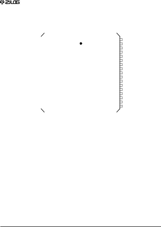
Figure 3. 68-Pin PLCC Z89323/373 Pin Configuration
VSS /RES WAIT P25/UI2 P22/UO0 P26 CLKO CLKI P24/UO2 /DS P23/UO1 VDD
NC
EA2
EA1
EA0
HALT
4 |
DS95DSP0101 Q4/95 |

P R E L I M I N A R Y |
Z89323/373/393 |
16-BIT DIGITAL SIGNAL PROCESSORS |
Table 2. 68-Pin PLCC Z89323/373 Pin Description
No. |
Symbol |
Function |
Direction |
|
|
|
|
1 |
P12/SIN |
Port12/SerialInput |
In/Output |
2 |
P20/INT0 |
Port20/Interrupt0 |
In/Output |
3 |
EXT12/P012 |
ExtData12/Port012 |
In/Output |
4 |
EXT13/P013 |
ExtData13/Port013 |
In/Output |
5 |
VDD |
Power |
|
|
|
|
|
6 |
EXT14/P014 |
ExtData14/Port014 |
In/Output |
7 |
VSS |
Ground |
In/Output |
8 |
EXT15/P015 |
ExtData15/Port015 |
|
9 |
NC |
NoConnection |
|
10 |
NC |
NoConnection |
|
|
|
|
|
11 |
EXT3/P03 |
ExtData3/Port03 |
In/Output |
12 |
EXT4/P04 |
ExtData4/Port04 |
In/Output |
13 |
VSS |
Ground |
|
14 |
VDD |
Power |
In/Output |
15 |
EXT5/P05 |
ExtData5/Port05 |
|
|
|
|
|
16 |
P13/SOUT |
Port13/SerialOutput |
In/Output |
17 |
EXT6/P06 |
ExtData6/Port06 |
In/Output |
18 |
P14/SS |
Port14/SerialSelect |
In/Output |
19 |
EXT7/P07 |
ExtData7/Port07 |
In/Output |
20 |
P15/SK |
Port15/SerialClock |
In/Output |
|
|
|
|
21 |
P27 |
Port27 |
In/Output |
22 |
EXT8/P08 |
ExtData8/Port08 |
In/Output |
23 |
EXT9/P09 |
ExtData9/Port09 |
In/Output |
24 |
VSS |
Ground |
|
25 |
EXT10/P010 |
ExtData10/Port010 |
In/Output |
26 |
VSS |
Ground |
In/Output |
27 |
EXT11/P011 |
ExtData11/Port011 |
|
28 |
VDD |
Power |
Input |
29 |
VAHI |
AnalogHighRef. |
|
|
|
|
|
30 |
VSS |
Ground |
In/Output |
31 |
P16/UI0 |
Port16/UserInput0 |
|
32 |
VALO |
AnalogLowRef. |
Input |
33 |
P17/UI1 |
Port17/UserInput1 |
In/Output |
34 |
ANGND |
AnalogGround |
Input |
|
|
|
|
No. |
Symbol |
Function |
Direction |
|
|
|
|
35 |
AN0 |
A/DInput0 |
Input |
36 |
AN1 |
A/DInput1 |
Input |
37 |
AN2 |
A/DInput2 |
Input |
38 |
AN3 |
A/DInput3 |
Input |
39 |
VSS |
Ground |
|
40 |
P21/INT1 |
Port21/Interrupt1 |
In/Output |
41 |
ANVCC |
AnalogPower |
Input |
42 |
VDD |
Power |
Input |
43 |
RD//WR |
R/WExternalBus |
Output |
44 |
HALT |
HaltExecution |
Input |
|
|
|
|
45 |
EA0 |
ExtAddress0 |
Output |
46 |
EA1 |
ExtAddress1 |
Output |
47 |
EA2 |
ExtAddress2 |
Output |
48 |
NC |
NoConnection |
|
49 |
VDD |
Power |
|
50 |
P23/UO1 |
Port23/UserOutput1 |
In/Output |
51 |
/DS |
ExtDataStrobe |
Output |
52 |
P24/UO2 |
Port24/UserOutput2 |
In/Output |
53 |
CLKI |
Clock/CrystalIn |
Input |
54 |
CLKO |
Clock/CrystalOut |
Input |
|
|
|
|
55 |
P26 |
Port26 |
In/Output |
56 |
P22/UO0 |
Port22/UserOutput0 |
In/Output |
57 |
P25/UI2 |
Port25/UserInput2 |
In/Output |
58 |
WAIT |
WaitforExt |
Input |
|
|
|
|
59 |
/RES |
Reset |
Input |
60 |
VSS |
Ground |
|
61 |
VDD |
Power |
|
62 |
VSS |
Ground |
In/Output |
63 |
EXT0/P00 |
ExtData0/Port00 |
|
|
|
|
|
64 |
EXT1/P01 |
ExtData1/Port01 |
In/Output |
65 |
EXT2/P02 |
ExtData2/Port02 |
In/Output |
66 |
P10/INT2 |
Port10/Interrupt2 |
In/Output |
67 |
VSS |
Ground |
In/Output |
68 |
P11/CLKOUT |
Port11/ClockOutput |
|
|
|
|
|
DS95DSP0101 Q4/95 |
5 |
P R E L I M I N A R Y |
Z89323/373/393 |
16-BIT DIGITAL SIGNAL PROCESSORS |
PIN DESCRIPTION (Continued)
|
|
|
|
|
EXT15/P015 |
|
VSS |
|
EXT14/P014 |
|
EXT13/P013 |
|
EXT12/P012 |
|
P20/INT0 |
|
VSS |
|
EXT2/P02 |
|
EXT1/P01 |
|
EXT0/P00 |
|
VSS |
|
|
|
|
|||
|
|
|
|
|
|
|
|
|
|
|
|
|
|
|
|
|
||||||||||||||||
|
|
|
|
|
|
|
|
|
|
|
|
|
|
|
|
|
|
|
|
|
|
|
|
|
|
|
|
|
|
|
|
|
|
|
|
|
|
|
|
|
|
|
|
|
|
|
|
|
|
|
|
|
|
|
|
|
|
|
|
|
|
|
|
|
|
|
|
|
|
|
|
|
|
|
|
|
|
|
|
|
|
|
|
|
|
|
|
|
|
|
|
|
|
|
|
|||
|
44 |
43 |
42 |
41 |
40 |
39 38 |
|
37 |
36 |
35 |
34 |
|
|
|
|
|
||||||||||||||||
EXT3/P03 |
|
|
|
1 |
|
|
|
|
|
|
|
|
|
|
|
|
|
|
|
|
|
|
|
|
|
33 |
|
|
|
/RES |
||
|
|
|
|
|
|
|
|
|
|
|
|
|
|
|
|
|
|
|
|
|
|
|
|
|
|
|||||||
EXT4/P04 |
|
2 |
|
|
|
|
|
|
|
|
|
|
|
|
|
|
|
|
|
|
|
|
|
32 |
|
|
|
WAIT |
||||
|
|
|
|
|
|
|
|
|
|
|
|
|
|
|
|
|
|
|
|
|
|
|
|
|
|
|||||||
VSS |
|
3 |
|
|
|
|
|
|
|
|
|
|
|
|
|
|
|
|
|
|
|
|
|
31 |
|
|
|
P24/UO2 |
||||
|
|
|
|
|
|
|
|
|
|
|
|
|
|
|
|
|
|
|
|
|
|
|
|
|
|
|||||||
EXT5/P05 |
|
4 |
|
|
|
|
|
|
|
|
|
|
|
|
|
|
|
|
|
|
|
|
|
30 |
|
|
|
P22/UO0 |
||||
|
|
|
|
|
|
|
|
|
|
|
|
|
|
|
|
|
|
|
|
|
|
|
|
|
|
|||||||
EXT6/P06 |
|
5 |
|
|
|
|
|
|
Z89323/373 |
|
|
|
|
|
|
29 |
|
|
|
CLK0 |
||||||||||||
|
|
|
|
|
|
|
|
|
|
|
|
|
|
|
|
|
||||||||||||||||
EXT7/P07 |
|
|
|
6 |
|
|
|
|
|
|
|
|
|
|
|
|
28 |
|
|
|
CLK1 |
|||||||||||
|
|
|
|
|
|
|
|
|
44-Pin QFP |
|
|
|
|
|
|
|
|
|
||||||||||||||
INT1/P21 |
|
|
|
7 |
|
|
|
|
|
|
|
|
|
|
|
|
27 |
|
|
|
/DS |
|||||||||||
|
|
|
|
|
|
|
|
|
|
|
|
|
|
|
|
|
|
|
|
|
|
|
|
|
|
|
||||||
EXT8/P08 |
|
8 |
|
|
|
|
|
|
|
|
|
|
|
|
|
|
|
|
|
|
|
|
|
26 |
|
|
|
P23/UO1 |
||||
|
|
|
|
|
|
|
|
|
|
|
|
|
|
|
|
|
|
|
|
|
|
|
|
|
|
|||||||
EXT9/P09 |
|
9 |
|
|
|
|
|
|
|
|
|
|
|
|
|
|
|
|
|
|
|
|
|
25 |
|
|
|
EA2 |
||||
|
|
|
|
|
|
|
|
|
|
|
|
|
|
|
|
|
|
|
|
|
|
|
|
|
|
|||||||
VSS |
|
10 |
|
|
|
|
|
|
|
|
|
|
|
|
|
|
|
|
|
|
|
|
|
24 |
|
|
|
EA1 |
||||
|
|
|
|
|
|
|
|
|
|
|
|
|
|
|
|
|
|
|
|
|
|
|
|
|
|
|||||||
EXT10/P010 |
|
11 |
|
|
|
|
|
|
|
|
|
|
|
|
|
|
|
|
|
|
|
|
|
23 |
|
|
|
EA0 |
||||
|
|
|
|
|
|
|
|
|
|
|
|
|
|
|
|
|
|
|
|
|
|
|
|
|
|
|||||||
|
12 |
13 |
14 |
15 |
16 |
|
17 |
18 |
|
19 |
20 |
21 |
22 |
|
|
|
|
|
||||||||||||||
|
|
|
|
|
|
|
|
|
|
|
|
|
|
|
|
|
|
|
|
|
|
|
|
|
|
|
|
|
|
|
|
|
|
|
|
|
|
|
|
|
|
|
|
|
|
|
|
|
|
|
|
|
|
|
|
|
|
|
|
|
|
|
|
|
|
|
|
|
|
|
|
|
|
|
|
|
|
|
|
|
|
|
|
|
|
|
|
|
|
|
|
|
|
|
|
|
|
|
|
|
|
|
|
|
|
|
|
|
|
|
|
|
|
|
|
|
|
|
|
|
|
|
|
|
|
|
|
|
|
|
|
|
|
|
|
|
EXT11/P011 |
|
VAHI |
|
VALO |
|
ANGND |
|
AN0 |
|
AN1 |
|
AN2 |
|
AN3 |
|
ANVCC |
|
VDD |
|
RD//WR |
|
|
|
|
|||
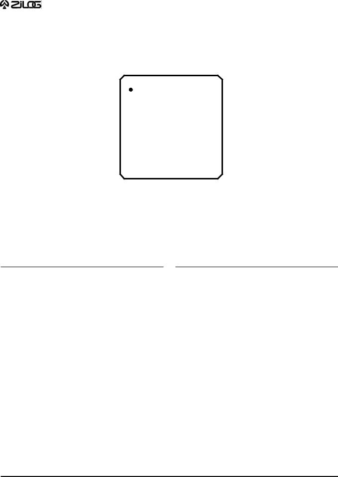
Figure 4. 44-Pin QFP Z89323/373 Pin Configuration
Table 3. 44-Pin QFP Z89323/373 Pin Description
No. |
Symbol |
Function |
Direction |
|
|
|
|
1 |
EXT3/P03 |
ExtData3/Port03 |
In/Output |
2 |
EXT4/P04 |
ExtData4/Port04 |
In/Output |
3 |
VSS |
Ground |
In/Output |
4 |
EXT5/P05 |
ExtData5/Port05 |
|
5 |
EXT6/P06 |
ExtData6/Port06 |
In/Output |
|
|
|
|
6 |
EXT7/P07 |
ExtData7/Port07 |
In/Output |
7 |
P21/INT1 |
Port21/Interrupt1 |
In/Output |
8 |
EXT8/P08 |
ExtData8/Port08 |
In/Output |
9 |
EXT9/P09 |
ExtData9/Port09 |
In/Output |
10 |
VSS |
Ground |
|
11 |
EXT10/P010 |
ExtData10/Port010 |
In/Output |
12 |
EXT11/P011 |
ExtData11/Port011 |
In/Output |
13 |
VAHI |
AnalogHighRef. |
Input |
14 |
VALO |
AnalogLowRef. |
Input |
15 |
ANGND |
AnalogGround |
Input |
16 |
AN0 |
A/DInput0 |
Input |
|
|
|
|
17 |
AN1 |
A/DInput1 |
Input |
18 |
AN2 |
A/DInput2 |
Input |
19 |
AN3 |
A/DInput3 |
Input |
20 |
ANVCC |
AnalogPower |
Input |
21 |
VDD |
Power |
Output |
22 |
RD//WR |
R/WExternalBus |
|
|
|
|
|
No. |
Symbol |
Function |
Direction |
|
|
|
|
23 |
EA0 |
ExtAddress0 |
Output |
24 |
EA1 |
ExtAddress1 |
Output |
25 |
EA2 |
ExtAddress2 |
Output |
26 |
P23/UO1 |
Port23/UserOutput1 |
In/Output |
27 |
/DS |
ExtDataStrobe |
Output |
|
|
|
|
28 |
CLKI |
Clock/CrystalIn |
Input |
29 |
CLKO |
Clock/CrystalOut |
Input |
30 |
P22/UO0 |
Port22/UserOutput0 |
In/Output |
31 |
P24/UO2 |
Port24/UserOutput2 |
In/Output |
32 |
WAIT |
WaitforExt |
Input |
|
|
|
|
33 |
/RES |
Reset |
Input |
34 |
VSS |
Ground |
In/Output |
35 |
EXT0/P00 |
ExtData0/Port00 |
|
36 |
EXT1/P01 |
ExtData1/Port01 |
In/Output |
37 |
EXT2/P02 |
ExtData2/Port02 |
In/Output |
38 |
VSS |
Ground |
|
39 |
P20/INT0 |
Port20/Interrupt0 |
In/Output |
40 |
EXT12/P012 |
ExtData12/Port012 |
In/Output |
41 |
EXT13/P013 |
ExtData13/Port013 |
In/Output |
42 |
EXT14/P014 |
ExtData14/Port014 |
In/Output |
43 |
VSS |
Ground |
In/Output |
44 |
EXT15/P015 |
ExtData15/Port015 |
|
|
|
|
|
6 |
DS95DSP0101 Q4/95 |
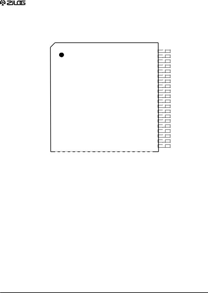
P R E L I M I N A R Y |
Z89323/373/393 |
16-BIT DIGITAL SIGNAL PROCESSORS |
|
|
|
|
|
|
|
P31 |
|
VSS |
|
EXT14/P014 |
|
VCC |
|
EXT13/P013 |
|
EXT12/P012 |
|
P20/INT0 |
|
P12/SIN |
|
P11/CLKOUT |
|
VSS |
|
P10/INT2 |
|
EXT2/P02 |
|
EXT1/P01 |
|
EXT0/P00 |
|
P30 |
|
VSS |
|
NC |
|
VCC |
|
VSS |
|
/RES |
|
|
|
|
|
|
|
|
|
|
|
|
|
|
|
|
|
|
|
|
|
|
|
|
|
|
|
|
|
|
|
|
|
|
|
|
|
|
|
|
|
|
|
|
|
|||
|
|
|
|
|
|
|
|
|
|
|
|
|
|
|
|
|
|
|
|
|
|
|
|
|
|
|
|
|
|
|
|
|
|
|
|
|
|
|
|
|
|
|
|
|
|
|
|
|
|
|
|
|
|
|
|
|
|
|
|
|
|
|
|
|
|
|
|
|
|
|
|
|
|
|
|
|
|
|
|
|
|
|
|
|
|
|
|
|
|
|
|
|
|
|
|
|
|
|
|
|
|
|
|
|
|
|
|
|
|
|
|
|
|
|
|
|
|
|
|
|
|
|
|
|
|
|
|
|
|
|
|
|
|
|
|
|
|
|
|
|
|
|
80 |
79 |
78 |
77 |
76 |
75 |
74 |
73 |
72 |
71 |
70 |
69 |
68 |
67 |
66 |
65 |
64 |
63 |
62 |
61 |
|
||||||||||||||||||||||||
NC |
|
|
|
1 |
|
|
|
|
|
|
|
|
|
|
|
|
|
|
|
|
|
|
|
|
|
|
|
|
|
|
|
|
|
|
|
|
|
|
|
|
|
|
60 |
|||
|
|
|
|
|
|
|
|
|
|
|
|
|
|
|
|
|
|
|
|
|
|
|
|
|
|
|
|
|
|
|
|
|
|
|
|
|
|
|
||||||||
EXT15/P015 |
|
|
|
2 |
|
|
|
|
|
|
|
|
|
|
|
|
|
|
|
|
|
|
|
|
|
|
|
|
|
|
|
|
|
|
|
|
|
|
|
|
|
|
59 |
|||
|
|
|
|
|
|
|
|
|
|
|
|
|
|
|
|
|
|
|
|
|
|
|
|
|
|
|
|
|
|
|
|
|
|
|
|
|
|
|
||||||||
|
|
|
|
|
|
|
|
|
|
|
|
|
|
|
|
|
|
|
|
|
|
|
|
|
|
|
|
|
|
|
|
|
|
|
|
|
|
|
||||||||
/EXTEN |
|
|
|
3 |
|
|
|
|
|
|
|
|
|
|
|
|
|
|
|
|
|
|
|
|
|
|
|
|
|
|
|
|
|
|
|
|
|
|
|
|
|
|
58 |
|||
|
|
|
|
|
|
|
|
|
|
|
|
|
|
|
|
|
|
|
|
|
|
|
|
|
|
|
|
|
|
|
|
|
|
|
|
|
|
|
||||||||
|
|
|
|
|
|
|
|
|
|
|
|
|
|
|
|
|
|
|
|
|
|
|
|
|
|
|
|
|
|
|
|
|
|
|
|
|
|
|
||||||||
NC |
|
|
|
4 |
|
|
|
|
|
|
|
|
|
|
|
|
|
|
|
|
|
|
|
|
|
|
|
|
|
|
|
|
|
|
|
|
|
|
|
|
|
|
57 |
|||
|
|
|
|
|
|
|
|
|
|
|
|
|
|
|
|
|
|
|
|
|
|
|
|
|
|
|
|
|
|
|
|
|
|
|
|
|
|
|
||||||||
|
|
|
|
|
|
|
|
|
|
|
|
|
|
|
|
|
|
|
|
|
|
|
|
|
|
|
|
|
|
|
|
|
|
|
|
|
|
|
||||||||
EXT3/P03 |
|
|
|
5 |
|
|
|
|
|
|
|
|
|
|
|
|
|
|
|
|
|
|
|
|
|
|
|
|
|
|
|
|
|
|
|
|
|
|
|
|
|
|
56 |
|||
|
|
|
|
|
|
|
|
|
|
|
|
|
|
|
|
|
|
|
|
|
|
|
|
|
|
|
|
|
|
|
|
|
|
|
|
|
|
|
||||||||
|
|
|
|
|
|
|
|
|
|
|
|
|
|
|
|
|
|
|
|
|
|
|
|
|
|
|
|
|
|
|
|
|
|
|
|
|
|
|
||||||||
P32 |
|
|
|
6 |
|
|
|
|
|
|
|
|
|
|
|
|
|
|
|
|
|
|
|
|
|
|
|
|
|
|
|
|
|
|
|
|
|
|
|
|
|
|
55 |
|||
|
|
|
|
|
|
|
|
|
|
|
|
|
|
|
|
|
|
|
|
|
|
|
|
|
|
|
|
|
|
|
|
|
|
|
|
|
|
|
||||||||
|
|
|
|
|
|
|
|
|
|
|
|
|
|
|
|
|
|
|
|
|
|
|
|
|
|
|
|
|
|
|
|
|
|
|
|
|
|
|
||||||||
EXT4/P04 |
|
|
|
7 |
|
|
|
|
|
|
|
|
|
|
|
|
|
|
|
|
|
|
|
|
|
|
|
|
|
|
|
|
|
|
|
|
|
|
|
|
|
|
54 |
|||
|
|
|
|
|
|
|
|
|
|
|
|
|
|
|
|
|
|
|
|
|
|
|
|
|
|
|
|
|
|
|
|
|
|
|
|
|
|
|
||||||||
|
|
|
|
|
|
|
|
|
|
|
|
|
|
|
|
|
|
|
|
|
|
|
|
|
|
|
|
|
|
|
|
|
|
|
|
|
|
|
||||||||
VSS |
|
|
|
8 |
|
|
|
|
|
|
|
|
|
|
|
|
|
|
|
|
|
|
|
|
|
|
|
|
|
|
|
|
|
|
|
|
|
|
|
|
|
|
53 |
|||
|
|
|
|
|
|
|
|
|
|
|
|
|
|
|
|
|
|
|
|
|
|
|
|
|
|
|
|
|
|
|
|
|
|
|
|
|
|
|
||||||||
|
|
|
|
|
|
|
|
|
|
|
|
|
|
|
|
|
|
|
|
|
|
|
|
|
|
|
|
|
|
|
|
|
|
|
|
|
|
|
||||||||
VCC |
|
|
|
9 |
|
|
|
|
|
|
|
|
|
|
|
|
|
|
|
|
|
Z89323 |
|
|
|
|
|
|
|
|
|
|
|
|
|
|
52 |
|||||||||
|
|
|
|
|
|
|
|
|
|
|
|
|
|
|
|
|
|
|
|
|
|
|
|
|
|
|
|
|
|
|
|
|||||||||||||||
EXT5/P05 |
|
|
|
10 |
|
|
|
|
|
|
|
|
|
|
|
|
|
|
|
|
|
|
|
|
|
|
|
|
|
|
|
|
|
|
|
|||||||||||
|
|
|
|
|
|
|
|
|
|
|
|
|
|
|
|
|
|
|
|
|
|
|
|
|
|
|
|
|
|
|
|
|
|
51 |
||||||||||||
|
|
|
|
|
|
|
|
|
|
|
|
|
|
|
|
|
|
|
|
|
|
|
|
|
|
|
|
|
|
|
|
|
||||||||||||||
|
|
|
|
|
|
|
|
|
|
|
|
|
|
|
|
|
|
|
80-Pin QFP |
|
|
|
|
|
|
|
|
|
|
|
|
|||||||||||||||
P13/SOUT |
|
|
|
11 |
|
|
|
|
|
|
|
|
|
|
|
|
|
|
|
|
|
|
|
|
|
|
|
|
|
|
|
|
50 |
|||||||||||||
|
|
|
|
|
|
|
|
|
|
|
|
|
|
|
|
|
|
|
|
|
|
|
|
|
|
|
|
|
|
|
||||||||||||||||
|
|
|
|
|
|
|
|
|
|
|
|
|
|
|
|
|
|
|
|
|
|
|
|
|
|
|
|
|
|
|
|
|
|
|
|
|
|
|
|
|
||||||
|
|
|
12 |
|
|
|
|
|
|
|
|
|
|
|
|
|
|
|
|
|
|
|
|
|
|
|
|
|
|
|
|
|
|
|
|
|
|
|
|
|
|
|||||
EXT6/P06 |
|
|
|
|
|
|
|
|
|
|
|
|
|
|
|
|
|
|
|
|
|
|
|
|
|
|
|
|
|
|
|
|
|
|
|
|
|
|
|
|
|
|
49 |
|||
|
|
|
|
|
|
|
|
|
|
|
|
|
|
|
|
|
|
|
|
|
|
|
|
|
|
|
|
|
|
|
|
|
|
|
|
|
|
|
|
|||||||
|
|
|
|
|
|
|
|
|
|
|
|
|
|
|
|
|
|
|
|
|
|
|
|
|
|
|
|
|
|
|
|
|
|
|
|
|
|
|
|
|||||||
P14/SS |
|
|
|
|
13 |
|
|
|
|
|
|
|
|
|
|
|
|
|
|
|
|
|
|
|
|
|
|
|
|
|
|
|
|
|
|
|
|
|
|
|
|
|
|
48 |
||
|
|
|
|
|
14 |
|
|
|
|
|
|
|
|
|
|
|
|
|
|
|
|
|
|
|
|
|
|
|
|
|
|
|
|
|
|
|
|
|
|
|
|
|
|
|||
|
|
|
|
|
|
|
|
|
|
|
|
|
|
|
|
|
|
|
|
|
|
|
|
|
|
|
|
|
|
|
|
|
|
|
|
|
|
|
|
|
|
|
||||
EXT7/P07 |
|
|
|
|
|
|
|
|
|
|
|
|
|
|
|
|
|
|
|
|
|
|
|
|
|
|
|
|
|
|
|
|
|
|
|
|
|
|
|
|
47 |
|||||
|
|
|
|
|
|
|
|
|
|
|
|
|
|
|
|
|
|
|
|
|
|
|
|
|
|
|
|
|
|
|
|
|
|
|
|
|
|
|
|
|||||||
P15/SK |
|
|
15 |
|
|
|
|
|
|
|
|
|
|
|
|
|
|
|
|
|
|
|
|
|
|
|
|
|
|
|
|
|
|
|
|
|
|
|
|
|
|
46 |
||||
|
|
|
|
|
|
|
|
|
|
|
|
|
|
|
|
|
|
|
|
|
|
|
|
|
|
|
|
|
|
|
|
|
|
|
|
|
|
|
|
|||||||
|
|
|
|
|
|
|
|
|
|
|
|
|
|
|
|
|
|
|
|
|
|
|
|
|
|
|
|
|
|
|
|
|
|
|
|
|
|
|
|
|||||||
|
|
16 |
|
|
|
|
|
|
|
|
|
|
|
|
|
|
|
|
|
|
|
|
|
|
|
|
|
|
|
|
|
|
|
|
|
|
|
|
|
|
|
|
|
|||
P27 |
|
|
|
|
|
|
|
|
|
|
|
|
|
|
|
|
|
|
|
|
|
|
|
|
|
|
|
|
|
|
|
|
|
|
|
|
|
|
|
|
45 |
|||||
|
|
|
|
|
|
|
|
|
|
|
|
|
|
|
|
|
|
|
|
|
|
|
|
|
|
|
|
|
|
|
|
|
|
|
|
|
|
|
|
|||||||
|
|
17 |
|
|
|
|
|
|
|
|
|
|
|
|
|
|
|
|
|
|
|
|
|
|
|
|
|
|
|
|
|
|
|
|
|
|
|
|
|
|
|
|
|
|||
EXT8/P08 |
|
|
|
|
|
|
|
|
|
|
|
|
|
|
|
|
|
|
|
|
|
|
|
|
|
|
|
|
|
|
|
|
|
|
|
|
|
|
|
|
44 |
|||||
|
|
|
|
|
|
|
|
|
|
|
|
|
|
|
|
|
|
|
|
|
|
|
|
|
|
|
|
|
|
|
|
|
|
|
|
|
|
|
|
|||||||
EXT9/P09 |
|
|
18 |
|
|
|
|
|
|
|
|
|
|
|
|
|
|
|
|
|
|
|
|
|
|
|
|
|
|
|
|
|
|
|
|
|
|
|
|
|
|
43 |
||||
|
|
|
|
|
|
|
|
|
|
|
|
|
|
|
|
|
|
|
|
|
|
|
|
|
|
|
|
|
|
|
|
|
|
|
|
|
|
|
|
|||||||
|
|
|
|
|
|
|
|
|
|
|
|
|
|
|
|
|
|
|
|
|
|
|
|
|
|
|
|
|
|
|
|
|
|
|
|
|
|
|
|
|||||||
VSS |
|
|
19 |
|
|
|
|
|
|
|
|
|
|
|
|
|
|
|
|
|
|
|
|
|
|
|
|
|
|
|
|
|
|
|
|
|
|
|
|
|
|
42 |
||||
|
|
|
|
|
|
|
|
|
|
|
|
|
|
|
|
|
|
|
|
|
|
|
|
|
|
|
|
|
|
|
|
|
|
|
|
|
|
|
|
|||||||
|
|
|
|
|
|
|
|
|
|
|
|
|
|
|
|
|
|
|
|
|
|
|
|
|
|
|
|
|
|
|
|
|
|
|
|
|
|
|
|
|||||||
|
|
20 |
|
|
|
|
|
|
|
|
|
|
|
|
|
|
|
|
|
|
|
|
|
|
|
|
|
|
|
|
|
|
|
|
|
|
|
|
|
|
41 |
|||||
P33 |
|
|
|
|
22 |
|
23 |
|
24 |
|
25 |
|
26 |
|
27 |
|
28 |
|
29 |
|
30 |
|
31 |
|
32 |
|
33 |
|
34 |
35 |
|
36 |
|
37 |
|
38 |
|
39 |
|
|||||||
|
|
21 |
|
|
|
|
|
|
|
|
|
|
|
|
|
|
|
|
|
|
40 |
|
|
|||||||||||||||||||||||
|
|
|
|
|
|
|
|
|
|
|
|
|
|
|
|
|
|
|
|
|
|
|
|
|
|
|
|
|
|
|
|
|
|
|
|
|
|
|
|
|
|
|
|
|
|
|
|
|
|
|
|
|
|
|
|
|
|
|
|
|
|
|
|
|
|
|
|
|
|
|
|
|
|
|
|
|
|
|
|
|
|
|
|
|
|
|
|
|
|
|
|
|
|
|
|
|
|
|
|
|
|
|
|
|
|
|
|
|
|
|
|
|
|
|
|
|
|
|
|
|
|
|
|
|
|
|
|
|
|
|
|
|
|
|
|
|
|
|
|
|
|
|
|
|
|
|
|
|
|
|
|
|
|
|
|
|
|
|
|
|
|
|
|
|
|
|
|
|
|
|
|
|
|
|
|
|
|
|
|
|
|
|
|
|
|
|
|
|
|
|
|
|
|
EXT10/P010 |
VSS |
NC |
P34 |
EXT11/P011 |
VCC |
VAHI |
VSS |
P16/UI0 |
VAL0 |
P17/UI1 |
ANGND |
AN0 |
AN1 |
AN2 |
AN3 |
VSS |
INT1/P21 |
ANVCC |
VCC |
|||||||||||||||||||||
Figure 4a. 80-Pin QFP Z89323/373 Pin Configuration
P37
WAIT P25/UI2 P22/UO0 P26 CLKO CLKI P24/U02 /DS P23/U01 VCC
NC
EA2
EA1
P36
EA0
HALT NC P35 RD//WR
DS95DSP0101 Q4/95 |
7 |

P R E L I M I N A R Y |
Z89323/373/393 |
16-BIT DIGITAL SIGNAL PROCESSORS |
PIN DESCRIPTION (Continued)
Table 4a. 80-Pin QFP Z89323/373 Pin Description
No. |
Symbol |
Function |
Direction |
|
|
|
|
1 |
NC |
NoConnection |
|
2 |
EXT15/P015 |
ExtData15/Port015 |
In/Output |
3 |
/EXTEN |
ExtEnable |
Input |
4 |
NC |
NoConnection |
|
5 |
EXT3/P03 |
ExtData3/Port03 |
In/Output |
6 |
P32 |
Port32 |
Input |
7 |
EXT4/P04 |
ExtData4/Port04 |
In/Output |
8 |
VSS |
Ground |
|
9 |
VDD |
Power |
In/Output |
10 |
EXT5/P05 |
ExtData5/Port05 |
|
|
|
|
|
11 |
P13/SOUT |
Port13/SerialOutput |
In/Output |
12 |
EXT6/P06 |
ExtData6/Port06 |
In/Output |
13 |
P14/SS |
Port14/SerialSelect |
In/Output |
14 |
EXT7/P07 |
ExtData7/Port07 |
In/Output |
15 |
P15/SK |
Port15/SerialClock |
In/Output |
16 |
P27 |
Port27 |
In/Output |
17 |
EXT8/P08 |
ExtData8/Port08 |
In/Output |
18 |
EXT9/P09 |
ExtData9/Port09 |
In/Output |
19 |
VSS |
Ground |
Input |
20 |
P33 |
Port33 |
|
|
|
|
|
21 |
EXT10/P010 |
ExtData10/Port010 |
In/Output |
22 |
VSS |
Ground |
|
23 |
NC |
NoConnection |
|
24 |
P34 |
Port34 |
Output |
25 |
EXT11/P011 |
ExtData11/Port011 |
In/Output |
26 |
VDD |
Power |
Input |
27 |
VAHI |
AnalogHighRef. |
|
28 |
VSS |
Ground |
In/Output |
29 |
P16/UI0 |
Port16/UserInput0 |
|
30 |
VAL0 |
AnalogLowRef. |
Input |
|
|
|
|
31 |
P17/UI1 |
Port17/UserInput1 |
In/Output |
32 |
ANGND |
AnalogGround |
Input |
33 |
AN0 |
A/DInput0 |
Input |
34 |
AN1 |
A/DInput1 |
Input |
35 |
AN2 |
A/DInput2 |
Input |
36 |
AN3 |
A/DInput3 |
Input |
37 |
VSS |
Ground |
In/Output |
38 |
P21/INT1 |
Port21/Interrupt1 |
|
39 |
ANVCC |
AnalogPower |
Input |
40 |
VDD |
Power |
Input |
No. |
Symbol |
Function |
Direction |
|
|
|
|
41 |
RD//WR |
R/WExternalBus |
Output |
42 |
P35 |
Port35 |
Output |
43 |
NC |
NoConnection |
|
44 |
HALT |
HaltExecution |
Input |
45 |
EA0 |
ExtAddress0 |
Output |
46 |
P36 |
Port36 |
Output |
47 |
EA1 |
ExtAddress1 |
Output |
48 |
EA2 |
ExtAddress2 |
Output |
49 |
NC |
NoConnection |
|
50 |
VDD |
Power |
|
51 |
P23/UO1 |
Port23/UserOutput1 |
In/Output |
52 |
/DS |
ExtDataStrobe |
Output |
53 |
P24/UO2 |
Port24/UserOutput2 |
In/Output |
54 |
CLKI |
Clock/CrystalIn |
Input |
55 |
CLKO |
Clock/CrystalOut |
Input |
56 |
P26 |
Port26 |
In/Output |
57 |
P22/UO0 |
Port22/UserOutput0 |
In/Output |
58 |
P25/UI2 |
Port25/UserInput2 |
In/Output |
59 |
WAIT |
WaitforExt |
Input |
60 |
P37 |
Port37 |
Output |
|
|
|
|
61 |
/RES |
Reset |
Input |
62 |
VSS |
Ground |
|
63 |
VDD |
Power |
|
64 |
NC |
NoConnection |
|
65 |
VSS |
Ground |
Input |
66 |
P30 |
Port30 |
|
67 |
EXT0/P00 |
ExtData0/Port00 |
In/Output |
68 |
EXT1/P01 |
ExtData1/Port01 |
In/Output |
69 |
EXT2/P02 |
ExtData2/Port02 |
In/Output |
70 |
P10/INT2 |
Port10/Interrupt2 |
In/Output |
|
|
|
|
71 |
VSS |
Ground |
In/Output |
72 |
P11/CLKOUT |
Port11/ClockOutput |
|
73 |
P12/SIN |
Port12/SerialInput |
In/Output |
74 |
P20/INT0 |
Port20/Interrupt0 |
In/Output |
75 |
EXT12/P012 |
ExtData12/Port012 |
In/Output |
76 |
EXT13/P013 |
ExtData13/Port013 |
In/Output |
77 |
VDD |
Power |
In/Output |
78 |
EXT14/P014 |
ExtData14/Port014 |
|
79 |
VSS |
Ground |
Input |
80 |
P31 |
Port31 |
|
|
|
|
|
8 |
DS95DSP0101 Q4/95 |

/EXTEN
EXT3/P03
PA8
EXT4/P04
PA9
VSS
VDD EXT5/P05 PA10 SOUT/P13 EXT6/P06 PA11 SS/P14 EXT7/P07 SK/P15 P27 PA12 EXT8/P08 PA13 EXT9/P09 PA14 VSS PA15
EXT10/P010 VSS
|
|
|
|
|
|
|
P R E L I M I N A R Y |
|
|
|
|
|
|
|
Z89323/373/393 |
|||||||||
|
|
|
|
|
|
|
|
|
|
|
|
|
16-BIT DIGITAL SIGNAL PROCESSORS |
|||||||||||
/PAZ |
EXT15/P015 |
PA7 |
VSS |
PA6 |
EXT14/P14 |
VDD |
EXT13/P013 |
PA5 |
EXT12/P012 |
PA4 |
P20/INT0 |
P12/SIN |
P11/CLKOUT |
VSS |
PA3 |
P10/INT2 |
EXT2/P02 |
PA2 |
EXT1/P01 |
PA1 |
EXT0/P00 |
PA0 |
VSS |
VDD |
|
|
|
|
|
|
|
|
|
|
|
|
|
|
|
|
|
|
|
|
|
|
|
|
|
|
|
|
|
|
|
|
|
|
|
|
|
|
|
|
|
|
|
|
|
|
|
|
|
|
|
|
|
|
|
|
|
|
|
|
|
|
|
|
|
|
|
|
|
|
|
|
|
|
|
|
|
|
|
|
|
|
|
|
|
|
|
|
|
|
|
|
|
|
|
|
|
|
|
|
|
|
|
|
|
|
|
|
|
|
|
|
|
|
|
|
|
|
|
|
|
|
|
|
|
|
|
|
|
|
|
|
|
|
|
|
|
|
|
|
|
|
|
|
|
|
|
|
|
|
|
|
|
|
|
|
|
|
|
|
|
|
|
|
|
|
|
|
|
|
|
|
|
|
|
|
|
|
|
|
1 |
100 |
99 |
98 |
97 |
96 |
95 |
94 |
93 |
92 |
91 |
90 |
89 |
|
88 |
|
87 |
|
86 |
85 |
84 |
83 |
82 |
81 |
80 |
79 |
78 |
77 |
76 |
|
|
|
|
|
||||||||||||||||||||||
|
|
|
|
|
|
|
|
|
||||||||||||||||||||||||||||||||||||||||||||||||||
|
|
|
|
|
|
|
|
|
|
|
|
|
|
|
|
|
|
|
|
|
|
|
|
|
|
|
|
|
|
|
|
|
|
|
|
|
|
|
|
|
|
|
|
|
|
|
|
|
|
75 |
|
|
|
VSS |
||||
|
|
|
2 |
|
|
|
|
|
|
|
|
|
|
|
|
|
|
|
|
|
|
|
|
|
|
|
|
|
|
|
|
|
|
|
|
|
|
|
|
|
|
|
|
|
|
|
|
|
|
|
74 |
|
|
|
/RES |
|||
|
|
|
|
|
|
|
|
|
|
|
|
|
|
|
|
|
|
|
|
|
|
|
|
|
|
|
|
|
|
|
|
|
|
|
|
|
|
|
|
|
|
|
|
|
|
|
|
|
|
|
|
|
||||||
|
|
|
3 |
|
|
|
|
|
|
|
|
|
|
|
|
|
|
|
|
|
|
|
|
|
|
|
|
|
|
|
|
|
|
|
|
|
|
|
|
|
|
|
|
|
|
|
|
|
|
|
73 |
|
|
|
PD15 |
|||
|
|
|
|
|
|
|
|
|
|
|
|
|
|
|
|
|
|
|
|
|
|
|
|
|
|
|
|
|
|
|
|
|
|
|
|
|
|
|
|
|
|
|
|
|
|
|
|
|
|
|
|
|
||||||
|
|
|
4 |
|
|
|
|
|
|
|
|
|
|
|
|
|
|
|
|
|
|
|
|
|
|
|
|
|
|
|
|
|
|
|
|
|
|
|
|
|
|
|
|
|
|
|
|
|
|
|
72 |
|
|
|
WAIT |
|||
|
|
|
|
|
|
|
|
|
|
|
|
|
|
|
|
|
|
|
|
|
|
|
|
|
|
|
|
|
|
|
|
|
|
|
|
|
|
|
|
|
|
|
|
|
|
|
|
|
|
|
|
|
||||||
|
|
|
5 |
|
|
|
|
|
|
|
|
|
|
|
|
|
|
|
|
|
|
|
|
|
|
|
|
|
|
|
|
|
|
|
|
|
|
|
|
|
|
|
|
|
|
|
|
|
|
|
71 |
|
|
|
PD14 |
|||
|
|
|
|
|
|
|
|
|
|
|
|
|
|
|
|
|
|
|
|
|
|
|
|
|
|
|
|
|
|
|
|
|
|
|
|
|
|
|
|
|
|
|
|
|
|
|
|
|
|
|
|
|
||||||
|
|
|
6 |
|
|
|
|
|
|
|
|
|
|
|
|
|
|
|
|
|
|
|
|
|
|
|
|
|
|
|
|
|
|
|
|
|
|
|
|
|
|
|
|
|
|
|
|
|
|
|
70 |
|
|
|
P25/UI2 |
|||
|
|
|
|
|
|
|
|
|
|
|
|
|
|
|
|
|
|
|
|
|
|
|
|
|
|
|
|
|
|
|
|
|
|
|
|
|
|
|
|
|
|
|
|
|
|
|
|
|
|
|
|
|
||||||
|
|
|
7 |
|
|
|
|
|
|
|
|
|
|
|
|
|
|
|
|
|
|
|
|
|
|
|
|
|
|
|
|
|
|
|
|
|
|
|
|
|
|
|
|
|
|
|
|
|
|
|
69 |
|
|
|
PD13 |
|||
|
|
|
|
|
|
|
|
|
|
|
|
|
|
|
|
|
|
|
|
|
|
|
|
|
|
|
|
|
|
|
|
|
|
|
|
|
|
|
|
|
|
|
|
|
|
|
|
|
|
|
|
|
||||||
|
|
|
8 |
|
|
|
|
|
|
|
|
|
|
|
|
|
|
|
|
|
|
|
|
|
|
|
|
|
|
|
|
|
|
|
|
|
|
|
|
|
|
|
|
|
|
|
|
|
|
|
68 |
|
|
|
P22/UO0 |
|||
|
|
|
|
|
|
|
|
|
|
|
|
|
|
|
|
|
|
|
|
|
|
|
|
|
|
|
|
|
|
|
|
|
|
|
|
|
|
|
|
|
|
|
|
|
|
|
|
|
|
|
|
|
||||||
|
|
|
9 |
|
|
|
|
|
|
|
|
|
|
|
|
|
|
|
|
|
|
|
|
|
|
|
|
|
|
|
|
|
|
|
|
|
|
|
|
|
|
|
|
|
|
|
|
|
|
|
67 |
|
|
|
PD12 |
|||
|
|
|
|
|
|
|
|
|
|
|
|
|
|
|
|
|
|
|
|
|
|
|
|
|
|
|
|
|
|
|
|
|
|
|
|
|
|
|
|
|
|
|
|
|
|
|
|
|
|
|
|
|
||||||
|
|
|
10 |
|
|
|
|
|
|
|
|
|
|
|
|
|
|
|
|
|
|
|
|
|
|
|
|
|
|
|
|
|
|
|
|
|
|
|
|
|
|
|
|
|
|
|
|
|
|
|
66 |
|
|
|
P26 |
|||
|
|
|
|
|
|
|
|
|
|
|
|
|
|
|
|
|
|
|
|
|
|
|
|
|
|
|
|
|
|
|
|
|
|
|
|
|
|
|
|
|
|
|
|
|
|
|
|
|
|
|
|
|
||||||
|
|
|
11 |
|
|
|
|
|
|
|
|
|
|
|
|
|
|
|
|
|
|
|
|
|
|
|
|
|
|
|
|
|
|
|
|
|
|
|
|
|
|
|
|
|
|
|
|
|
|
|
65 |
|
|
|
CLKO |
|||
|
|
|
|
|
|
|
|
|
|
|
|
|
|
|
|
|
|
|
|
|
|
|
|
|
|
|
|
|
|
|
|
|
|
|
|
|
|
|
|
|
|
|
|
|
|
|
|
|
|
|
|
|
||||||
|
|
|
12 |
|
|
|
|
|
|
|
|
|
|
|
|
|
|
|
|
|
|
|
|
|
Z89393 |
|
|
|
|
|
|
|
|
|
|
|
|
|
|
|
|
|
|
|
64 |
|
|
|
CLKI |
|||||||||
|
|
|
|
|
|
|
|
|
|
|
|
|
|
|
|
|
|
|
|
|
|
|
|
|
|
|
|
|
|
|
|
|
|
|
|
|
|
|
|
|
|
|
|
|
|
|||||||||||||
|
|
|
|
|
|
|
|
|
|
|
|
|
|
|
|
|
|
|
|
|
|
|
|
|
|
|
|
|
|
|
|
|
|
|
|
|
|
|
|
|
|
|
|
|
|
|||||||||||||
|
|
|
13 |
|
|
|
|
|
|
|
|
|
|
|
|
|
|
|
|
|
|
|
|
|
|
|
|
|
|
|
|
|
|
|
|
|
|
|
|
|
|
|
|
63 |
|
|
|
P24/UO2 |
||||||||||
|
|
|
|
|
|
|
|
|
|
|
|
|
|
|
|
|
|
|
|
|
|
100-Pin QFP |
|
|
|
|
|
|
|
|
|
|
|
|
|
|
|
|
|
|
|
|
|
|||||||||||||||
|
|
|
14 |
|
|
|
|
|
|
|
|
|
|
|
|
|
|
|
|
|
|
|
|
|
|
|
|
|
|
|
|
|
|
|
|
|
|
|
|
|
62 |
|
|
|
PD11 |
|||||||||||||
|
|
|
|
|
|
|
|
|
|
|
|
|
|
|
|
|
|
|
|
|
|
|
|
|
|
|
|
|
|
|
|
|
|
|
|
|
|
|
|
|
|
|
|
|
|
|
|
|
|
|
|
|
||||||
|
|
|
15 |
|
|
|
|
|
|
|
|
|
|
|
|
|
|
|
|
|
|
|
|
|
|
|
|
|
|
|
|
|
|
|
|
|
|
|
|
|
|
|
|
|
|
|
|
|
|
|
61 |
|
|
|
/DS |
|||
|
|
|
|
|
|
|
|
|
|
|
|
|
|
|
|
|
|
|
|
|
|
|
|
|
|
|
|
|
|
|
|
|
|
|
|
|
|
|
|
|
|
|
|
|
|
|
|
|
|
|
|
|
||||||
|
|
|
16 |
|
|
|
|
|
|
|
|
|
|
|
|
|
|
|
|
|
|
|
|
|
|
|
|
|
|
|
|
|
|
|
|
|
|
|
|
|
|
|
|
|
|
|
|
|
|
|
60 |
|
|
|
P23/UO1 |
|||
|
|
|
|
|
|
|
|
|
|
|
|
|
|
|
|
|
|
|
|
|
|
|
|
|
|
|
|
|
|
|
|
|
|
|
|
|
|
|
|
|
|
|
|
|
|
|
|
|
|
|
|
|
||||||
|
|
|
|
|
|
|
|
|
|
|
|
|
|
|
|
|
|
|
|
|
|
|
|
|
|
|
|
|
|
|
|
|
|
|
|
|
|
|
|
|
|
|
|
|
|
|
|
|
|
|
|
|
||||||
|
|
|
17 |
|
|
|
|
|
|
|
|
|
|
|
|
|
|
|
|
|
|
|
|
|
|
|
|
|
|
|
|
|
|
|
|
|
|
|
|
|
|
|
|
|
|
|
|
|
|
|
59 |
|
|
|
PD10 |
|||
|
|
|
|
|
|
|
|
|
|
|
|
|
|
|
|
|
|
|
|
|
|
|
|
|
|
|
|
|
|
|
|
|
|
|
|
|
|
|
|
|
|
|
|
|
|
|
|
|
|
|
|
|
||||||
|
|
|
18 |
|
|
|
|
|
|
|
|
|
|
|
|
|
|
|
|
|
|
|
|
|
|
|
|
|
|
|
|
|
|
|
|
|
|
|
|
|
|
|
|
|
|
|
|
|
|
|
58 |
|
|
|
VDD |
|||
|
|
|
|
|
|
|
|
|
|
|
|
|
|
|
|
|
|
|
|
|
|
|
|
|
|
|
|
|
|
|
|
|
|
|
|
|
|
|
|
|
|
|
|
|
|
|
|
|
|
|
|
|
||||||
|
|
|
19 |
|
|
|
|
|
|
|
|
|
|
|
|
|
|
|
|
|
|
|
|
|
|
|
|
|
|
|
|
|
|
|
|
|
|
|
|
|
|
|
|
|
|
|
|
|
|
|
57 |
|
|
|
/ROMEN |
|||
|
|
|
|
|
|
|
|
|
|
|
|
|
|
|
|
|
|
|
|
|
|
|
|
|
|
|
|
|
|
|
|
|
|
|
|
|
|
|
|
|
|
|
|
|
|
|
|
|
|
|
|
|
||||||
|
|
|
20 |
|
|
|
|
|
|
|
|
|
|
|
|
|
|
|
|
|
|
|
|
|
|
|
|
|
|
|
|
|
|
|
|
|
|
|
|
|
|
|
|
|
|
|
|
|
|
|
56 |
|
|
|
EA2 |
|||
|
|
|
|
|
|
|
|
|
|
|
|
|
|
|
|
|
|
|
|
|
|
|
|
|
|
|
|
|
|
|
|
|
|
|
|
|
|
|
|
|
|
|
|
|
|
|
|
|
|
|
|
|
||||||
|
|
|
21 |
|
|
|
|
|
|
|
|
|
|
|
|
|
|
|
|
|
|
|
|
|
|
|
|
|
|
|
|
|
|
|
|
|
|
|
|
|
|
|
|
|
|
|
|
|
|
|
55 |
|
|
|
PD9 |
|||
|
|
|
|
|
|
|
|
|
|
|
|
|
|
|
|
|
|
|
|
|
|
|
|
|
|
|
|
|
|
|
|
|
|
|
|
|
|
|
|
|
|
|
|
|
|
|
|
|
|
|
|
|
||||||
|
|
|
22 |
|
|
|
|
|
|
|
|
|
|
|
|
|
|
|
|
|
|
|
|
|
|
|
|
|
|
|
|
|
|
|
|
|
|
|
|
|
|
|
|
|
|
|
|
|
|
|
54 |
|
|
|
EA1 |
|||
|
|
|
|
|
|
|
|
|
|
|
|
|
|
|
|
|
|
|
|
|
|
|
|
|
|
|
|
|
|
|
|
|
|
|
|
|
|
|
|
|
|
|
|
|
|
|
|
|
|
|
|
|
||||||
|
|
|
23 |
|
|
|
|
|
|
|
|
|
|
|
|
|
|
|
|
|
|
|
|
|
|
|
|
|
|
|
|
|
|
|
|
|
|
|
|
|
|
|
|
|
|
|
|
|
|
|
53 |
|
|
|
PD8 |
|||
|
|
|
|
|
|
|
|
|
|
|
|
|
|
|
|
|
|
|
|
|
|
|
|
|
|
|
|
|
|
|
|
|
|
|
|
|
|
|
|
|
|
|
|
|
|
|
|
|
|
|
|
|
||||||
|
|
|
24 |
|
|
|
|
|
|
|
|
|
|
|
|
|
|
|
|
|
|
|
|
|
|
|
|
|
|
|
|
|
|
|
|
|
|
|
|
|
|
|
|
|
|
|
|
|
|
|
52 |
|
|
|
EA0 |
|||
|
|
|
|
|
|
|
|
|
|
|
|
|
|
|
|
|
|
|
|
|
|
|
|
|
|
|
|
|
|
|
|
|
|
|
|
|
|
|
|
|
|
|
|
|
|
|
|
|
|
|
|
|
||||||
|
|
|
25 |
|
|
|
28 |
29 |
30 |
|
|
|
|
33 |
34 |
|
|
|
|
|
|
|
|
|
|
|
|
|
|
|
|
|
|
|
|
|
|
|
|
|
|
|
|
|
|
51 |
|
|
|
HALT |
||||||||
|
|
|
|
|
|
|
|
|
|
|
|
|
|
|
|
|
|
|
|
|
|
|
|
|
|
|
|
|
|
|
|
|
|
|
|
|
|
|
|
|
|
|
||||||||||||||||
|
|
|
|
|
26 |
27 |
31 |
32 |
35 |
36 |
37 |
|
38 |
|
39 |
|
40 |
41 |
42 |
43 |
44 |
45 |
46 |
47 |
48 |
49 |
50 |
|
|
|
|
|
||||||||||||||||||||||||||
|
|
|
|
|
|
|
|
|
|
|
|
|
|
|
|
|
|
|
|
|
|
|
|
|
|
|
|
|
|
|
|
|
|
|
|
|
|
|
|
|
|
|
|
|
|
|
|
|
|
|
|
|
|
|
|
|
|
|
|
|
|
|
|
|
|
|
|
|
|
|
|
|
|
|
|
|
|
|
|
|
|
|
|
|
|
|
|
|
|
|
|
|
|
|
|
|
|
|
|
|
|
|
|
|
|
|
|
|
|
|
|
|
|
|
|
|
|
|
|
|
|
|
|
|
|
|
|
|
|
|
|
|
|
|
|
|
|
|
|
|
|
|
|
|
|
|
|
|
|
|
|
|
|
|
|
|
|
|
|
|
|
|
|
|
|
|
|
|
|
|
|
|
|
|
|
|
|
|
|
|
|
|
|
|
|
|
|
|
|
|
|
|
|
|
|
|
|
|
|
|
|
|
|
|
|
|
|
|
|
|
|
|
|
|
|
|
|
|
|
|
|
|
|
|
|
|
|
|
|
|
|
|
|
|
|
PD0 |
EXT11/P011 |
PD1 |
VDD |
VAHI |
VSS |
UI0/P16 |
VALO |
UI1/P17 |
PD2 |
ANGND |
AN0 |
AN1 |
AN2 |
AN3 |
VSS |
INT1/P21 |
ANVCC |
PD3 |
VDD |
PD4 |
PD5 |
RD//WR |
PD6 |
PD7 |
Figure 5. 100-Pin QFP Z89393 Pin Configuration
DS95DSP0101 Q4/95 |
9 |

P R E L I M I N A R Y |
Z89323/373/393 |
16-BIT DIGITAL SIGNAL PROCESSORS |
PIN DESCRIPTION (Continued)
|
|
Table 4. 100-Pin QFP Z89393 Pin Description |
|
||
No. Symbol |
Function |
Direction |
No. Symbol |
Function |
Direction |
1 |
/EXTEN |
EXTEnable |
Input |
2 |
EXT3/P03 |
ExtData3/Port03 |
In/Output |
3 |
PA8 |
ProgramAddress8 |
Output |
4 |
EXT4/P04 |
ExtData4/Port04 |
In/Output |
5 |
PA9 |
ProgramAddress9 |
Output |
6 |
VSS |
Ground |
|
7 |
VDD |
Power |
In/Output |
8 |
EXT5/P05 |
ExtData5/Port05 |
|
9 |
PA10 |
ProgramAddress10 |
Output |
10 |
P13/SOUT |
Port13/SerialOutput |
In/Output |
|
|
|
|
11 |
EXT6/P06 |
ExtData6/Port06 |
In/Output |
12 |
PA11 |
ProgramAddress11 |
Output |
13 |
P14/SS |
Port14/SerialSelect |
In/Output |
14 |
EXT7/P07 |
ExtData7/Port07 |
In/Output |
15 |
P15/SK |
Port15/SerialClock |
In/Output |
16 |
P27 |
Port27 |
In/Output |
17 |
PA12 |
ProgramAddress12 |
Output |
18 |
EXT8/P08 |
ExtData8/Port08 |
In/Output |
19 |
PA13 |
ProgramAddress13 |
Output |
20 |
EXT9/P09 |
ExtData9/Port09 |
In/Output |
|
|
|
|
21 |
PA14 |
ProgramAddress14 |
Output |
22 |
VSS |
Ground |
Output |
23 |
PA15 |
ProgramAddress15 |
|
24 |
EXT10/P010 |
ExtData10/Port010 |
In/Output |
25 |
VSS |
Ground |
Input |
26 |
PD0 |
ProgramData0 |
|
27 |
EXT11/P011 |
ExtData11/Port011 |
In/Output |
28 |
PD1 |
ProgramData1 |
Input |
29 |
VDD |
Power |
Input |
30 |
VAHI |
AnalogHighRef. |
|
|
|
|
|
31 |
VSS |
Ground |
In/Output |
32 |
P16/UI0 |
Port16/UserInput0 |
|
33 |
VALO |
AnalogLowRef. |
Input |
34 |
P17/UI1 |
Port17/UserInput1 |
In/Output |
35 |
PD2 |
ProgramData2 |
Input |
36 |
ANGND |
AnalogGround |
Input |
37 |
AN0 |
A/DInput0 |
Input |
38 |
AN1 |
A/DInput1 |
Input |
39 |
AN2 |
A/DInput2 |
Input |
40 |
AN3 |
A/DInput3 |
Input |
|
|
|
|
41 |
VSS |
Ground |
In/Output |
42 |
P21/INT1 |
Port21/Interrupt1 |
|
43 |
ANVCC |
AnalogPower |
Input |
44 |
PD3 |
ProgramData3 |
Input |
45 |
VDD |
Power |
Input |
46 |
PD4 |
ProgramData4 |
|
47 |
PD5 |
ProgramData5 |
Input |
48 |
RD//WR |
R/WExternalBus |
Output |
49 |
PD6 |
ProgramData6 |
Input |
50 |
PD7 |
ProgramData7 |
Input |
|
|
|
|
51 |
HALT |
HaltExecution |
Input |
52 |
EA0 |
ExtAddress0 |
Output |
53 |
PD8 |
ProgramData8 |
Input |
54 |
EA1 |
ExtAddress1 |
Output |
55 |
PD9 |
ProgramData9 |
Input |
56 |
EA2 |
ExtAddress2 |
Output |
57 |
/ROMEN |
ROMEnable |
Input |
58 |
VDD |
Power |
Input |
59 |
PD10 |
ProgramData10 |
|
60 |
P23/UO1 |
Port23/UserOutput1 |
In/Output |
|
|
|
|
61 |
/DS |
ExtDataStrobe |
Output |
62 |
PD11 |
ProgramData11 |
Input |
63 |
P24/UO2 |
Port24/UserOutput2 |
In/Output |
64 |
CLKI |
Clock/CrystalIn |
Input |
65 |
CLKO |
Clock/CrystalOut |
Input |
66 |
P26 |
Port26 |
In/Output |
67 |
PD12 |
ProgramData12 |
Input |
68 |
P22/UO0 |
Port22/UserOutput0 |
In/Output |
69 |
PD13 |
ProgramData13 |
Input |
70 |
P25/UI2 |
Port25/UserInput2 |
In/Output |
|
|
|
|
71 |
PD14 |
ProgramData14 |
Input |
72 |
WAIT |
WaitforExt |
Input |
73 |
PD15 |
ProgramData15 |
Input |
74 |
/RES |
Reset |
Input |
75 |
VSS |
Ground |
|
76 |
VDD |
Power |
|
77 |
VSS |
Ground |
Output |
78 |
PA0 |
ProgramAddress0 |
|
79 |
EXT0/P00 |
ExtData0/Port00 |
In/Output |
80 |
PA1 |
ProgramAddress1 |
Output |
|
|
|
|
81 |
EXT1/P01 |
ExtData1/Port01 |
In/Output |
82 |
PA2 |
ProgramAddress2 |
Output |
83 |
EXT2/P02 |
ExtData2/Port02 |
In/Output |
84 |
P10/INT2 |
Port10/Interrupt2 |
In/Output |
85 |
PA3 |
ProgramAddress3 |
Output |
86 |
VSS |
Ground |
In/Output |
87 |
P11/CLKOUT |
Port11/ClockOutput |
|
88 |
P12/SIN |
Port12/SerialInput |
In/Output |
89 |
P20/INT0 |
Port20/Interrupt0 |
In/Output |
90 |
PA4 |
ProgramAddress4 |
Output |
|
|
|
|
91 |
EXT12/P012 |
ExtData12/Port012 |
In/Output |
92 |
PA5 |
ProgramAddress5 |
Output |
93 |
EXT13/P013 |
ExtData13/Port013 |
In/Output |
94 |
VDD |
Power |
In/Output |
95 |
EXT14/P014 |
ExtData14/Port014 |
|
96 |
PA6 |
ProgramAddress6 |
Output |
97 |
VSS |
Ground |
Output |
98 |
PA7 |
ProgramAddress7 |
|
99 |
EXT15/P015 |
ExtData15/Port015 |
In/Output |
100 |
/PAZ |
Tri-stateProgramBus |
Input |
|
|
|
|
10 |
DS95DSP0101 Q4/95 |
P R E L I M I N A R Y |
Z89323/373/393 |
16-BIT DIGITAL SIGNAL PROCESSORS |
PIN FUNCTIONS
CLKO-CLKI Clock (output/input). These pins act as the clock circuit input and output.
EXT15-EXT0 External Data Bus (input/output). These pins act as the data bus for user-defined outside registers, such as an ADC or DAC. The pins are normally tri-stated, except when the outside registers are specified as destination registers in the instructions. All the control signals exist to allow a read or a write through this bus. If user I/O Port 0
is enabled, these signals function as user Programmable I/O.
RD//WR Read/Write Strobe (output). This pin controls the data direction signal for the EXT-Bus. Data is available from the CPU on EXT15-EXT0 when this signal is Low. EXTBus is in input mode (high-impedance) when this signal is High.
EA2-EA0 External Address (output). These pins control the user-defined register address output (latched). One of eight user-defined external registers is selected by the processor with these address pins for read or write operations. Since the addresses are part of the processor memory map, the processor is simply executing internal reads and writes. External Addresses are used internally by the processor if the ADC, bit I/O (Port 0- 2), or SPI are enabled. (See the banks allocation of the EXT registers in Tables 6 and 7.)
/DS Data Strobe (output). This pin control the data strobe signal for EXT-Bus. Data is read by the external peripheral on the rising edge of /DS. Data is also read by the processor on the rising edge of CK.
HALT Halt State (input). This pin controls Stop Execution. The CPU continuously executes NOPs and the program counter remains at the same value when this pin is held High. An interrupt request must be executed (enabled) to exit HALT mode. After the interrupt service routine, the program continues from the instruction after the HALT (active high).
/INT0-/INT2 Three Interrupts (input, active on rising edge). These pins control interrupt requests 0-2. Interrupts are generated on the rising edge of the input signal. Interrupt vectors for the interrupt service starting address are stored in the following program memory locations:
Device |
/INT0 |
/INT1 |
/INT2 |
|
|
|
|
Z89323/373 |
1FFFH |
1FFEH |
1FFDH |
Z89393 |
FFFFH |
FFFEH |
FFFDH |
|
|
|
|
Priority is: INT2 = lowest, INT0 = highest. (Note: INT2 pin is not bonded out on the 44-pin QFP or PLCC packages.)
/RES Reset (input, active Low). This pin controls the asynchronous reset signal. The /RES signal must be kept Low for at least one clock cycle (clock output of the PLL block). The CPU pushes the contents of the Program Counter (PC) onto the stack and then fetches a new PC value from program memory address 0FFCH (or FFFCH for the Z89393) after the reset signal is released.
WAIT WAIT State (input). The wait signal is sampled at the rising edge of the clock with appropriate setup and hold times. The normal write cycle will continue when wait is inactive on a rising clock. A single wait-state can be generated internally by setting the appropriate bits in the wait state register (Bank 15/Ext 3) (active high).
P00-P015 Port 0 (input/output). These pins control Port 0 input and output when EXT I/F is not in use.
P10-P17 Port 1 (input/output). These pins are used for Port 1 programmable bit I/O when INT2, CLKOUT, SPI, or UI0-1 are not being used.
P20-P27 Port 2 (input/output). These pins control Port 2 input or output when UI2, UO0-2 or INT0-INT1 are not being used.
P30-P37 Port 3 Port3 (3:0) are four inputs and P3 (7:0) are four outputs.
UI1-UI0 Two Input Pins (input). These general-purpose input pins are directly tested by the conditional branch instructions. These are asynchronous input signals that have no special clock synchronization requirements.
UO1-UO0 Two Output Pins (output). These generalpurpose output pins reflect the value of two bits in the status register S5 and S6. These bits have no special significance and may be used to output data by writing to the status register. Note: The user output value is the opposite of the status register content.
SIN/SOUT. When enabled, these pins control SPI input and output.
AN0-AN3. These pins are used for Analog-to-Digital converter input.
ANGND and ANVCC. Analog to Digital ground and power supply.
DS95DSP0101 Q4/95 |
11 |

P R E L I M I N A R Y |
Z89323/373/393 |
16-BIT DIGITAL SIGNAL PROCESSORS |
PIN FUNCTIONS (Continued)
VAHI and VALO. Analog to Digital reference voltages.
/PAZ Tri-state Program Bus. This pin enables the Program Address bus for emulation purposes.
/EXTEN Ext Enable. This pin enables Ext output continuously for emulation purposes.
/ROMEN ROM Enable. This pin selects internal or external Program Memory.
ADDRESS SPACE
Program Memory. Programs of up to 8 Kwords can be masked into internal ROM (OTP for Z89373). Four locations are dedicated to the vector address for the three interrupts (IFFDH-IFFFH) and the starting address following a Reset (IFFCH). Internal ROM is mapped from 0000H to IFFFH, and the highest location for program is IFFBH.
Internal Data RAM. The Z89323 has an internal 512 x 16bit word data RAM organized as two banks of 256 x 16-bit words each: RAM0 and RAM1. Each data RAM bank is addressed by three pointers: Pn:0 (n = 0-2) for RAM0 and Pn:1 (n = 0-2) for RAM1. The RAM addresses for RAM0 and RAM1 are arranged from 0-255 and 256-511, respectively. The address pointers, which may be written to, or read from, are 8-bit registers connected to the lower byte of the internal 16-bit D-Bus and are used to perform modulo
addressing. Three addressing modes are available to access the Data RAM: register indirect, direct addressing, and short form direct. The contents of the RAM can be read to, or written from, in one machine cycle per word, without disturbing any internal registers or status other than the RAM address pointer used for each RAM. The contents of each RAM can be loaded simultaneously into the X and Y inputs of the multiplier.
Registers. The Z89323 has 19 internal registers and eight external registers and a secondary set of 15 peripheral control registers. Both external and internal registers are accessed in one machine cycle. The external registers are used to access the on-chip peripherals when they are enabled.
|
Data Memory |
|
|
|
Program Memory |
|||||
|
|
|
|
FFFF |
|
|
FFFF |
|
|
|
|
|
|
|
|
|
|
INT0-INT2 Vect. |
64 Kwords |
||
|
|
|
|
|
|
|
|
|
||
|
|
|
|
|
|
|
FFFC |
|
RESET Vector |
|
|
Not Used |
|
|
|
Not Used |
Or |
|
|
|
|
|
|
|
|
|
|
|
|
|
|
|
512 words |
|
|
|
01FF 4 Kwords |
|
|
|
|
|
|
DRAM1 |
|
|
INT0-INT2 Vect. |
0FFF |
|
|
|
|||
|
|
0100 |
|
|
|
|
||||
|
|
|
RESET Vector |
0FFC |
|
|
|
|||
|
|
|
|
|
|
|
|
|||
|
DRAM0 |
|
00FF |
|
|
|
|
|
|
|
|
|
|
|
|
|
|
|
|||
|
|
0000 |
|
|
0000 |
|
|
|
||
|
|
|
|
|
|
|
|
|
||
|
|
|
On-Chip Memory |
|
|
Off-Chip Memory |
||||
|
|
|
|
|
||||||
|
|
|
|
|
||||||
|
|
|
|
|
|
(Z89323/371) |
|
|
(Z89393) |
|
Figure 6. Memory Map
12 |
DS95DSP0101 Q4/95 |

P R E L I M I N A R Y |
Z89323/373/393 |
16-BIT DIGITAL SIGNAL PROCESSORS |
REGISTERS
The internal registers of the Z89323/373/393 are defined below:
Register |
Register Definition |
|
|
P |
Output of Multiplier, 24-bit |
XX Multiplier Input, 16-bit
YY Multiplier Input, 16-bit
AAccumulator, 24-bit
SR |
Status Register, 16-bit |
Pn:b |
Six Ram Address Pointers, 8-bit each |
P C |
Program Counter, 16-bit |
|
|
EXT 0 |
|
EXT 1 |
|
EXT 2 |
|
EXT 3 |
|
EXT 4 |
|
EXT 5 |
|
EXT 6 |
|
EXT 7 |
|
|
|
See Table 6 and Table 7 for the different assignments of EXT7-EXT0 in the different banks.
Register |
Register Definition |
|
|
EXTn |
External Registers, 16-bit |
BUS |
D-Bus |
Dn:b |
Eight Data Pointers* |
|
|
Note:
* These data pointers occupy the first four locations in RAM bank.
P holds the result of multiplications and is read-only.
X and Y are two 16-bit input registers for the multiplier. These registers can be utilized as temporary registers when the multiplier is not being used.
A is a 24-bit Accumulator. The output of the ALU is sent to this register. When 16-bit data is transferred into this register, it is placed into the 16 MSBs and the least significant eight bits are set to zero. Only the upper 16 bits are transferred to the destination register when the Accumulator is selected as a source register in transfer instructions.
Pn:b are the pointer registers for accessing data RAM, (n = 0,1,2 refer to the pointer number) (b = 0,1 refers to RAM Bank 0 or 1). They can be directly read from or written to, and can point to locations in data RAM or Program Memory.
EXTn are external registers (n = 0 to 7). There are eight 16bit registers provided here for mapping external devices into the address space of the processor. Note that the actual register RAM does not exist on the chip, but would exist as part of the internal or external device, such as an ADC.
BUS is a read-only register which, when accessed, returns the contents of the D-Bus. Bus is used for emulation only.
Dn:b refers to locations in RAM that can be used as a pointer to locations in program memory which is efficient for coefficient addressing. The programmer decides which location to choose from two bits in the status register and two bits in the operand. Thus, only the lower 16 possible locations in RAM can be specified. At any one time, there are eight usable pointers, four per bank, and the four pointers are in consecutive locations in RAM. For example, if S3/S4 = 01 in the status register, then D0:0/D1:0/D2:0/ D3:0 refer to register locations 4/5/6/7 in RAM Bank 0. Note that when the data pointers are being written to, a number is actually being loaded to Data RAM, so they can be used as a limited method for writing to RAM.
SR is the status register (Figure 8) which contains the ALU status and certain control bits (Table 5).
Table 5. Status Register Bit Functions
Status Register Bit |
Function |
|
||
|
|
|
||
S15 |
(N) |
ALU Negative |
||
S14 |
(OV) |
ALU Overflow |
||
S13 |
(Z) |
ALU Zero |
||
S12 |
(L) |
Carry |
|
|
S11 |
(UI1) |
User Input 1 |
||
S10 |
(UI0) |
User Input 0 |
||
|
|
|
||
S9 |
(SH3) |
MPY Output Arithmetically |
||
|
|
|
Shifted Right by three bits |
|
S8 |
(OP) |
Overflow |
Protection |
|
S7 |
(IE) |
Interrupt |
Enable |
|
S6 |
(UO1) |
User Output 1 |
||
S5 |
(UO0) |
User Output 0 |
||
S4-S3 |
“Short Form Direct” bits |
|||
S2-S0 (RPL) |
RAM Pointer Loop Size |
|||
|
|
|
|
|
DS95DSP0101 Q4/95 |
13 |
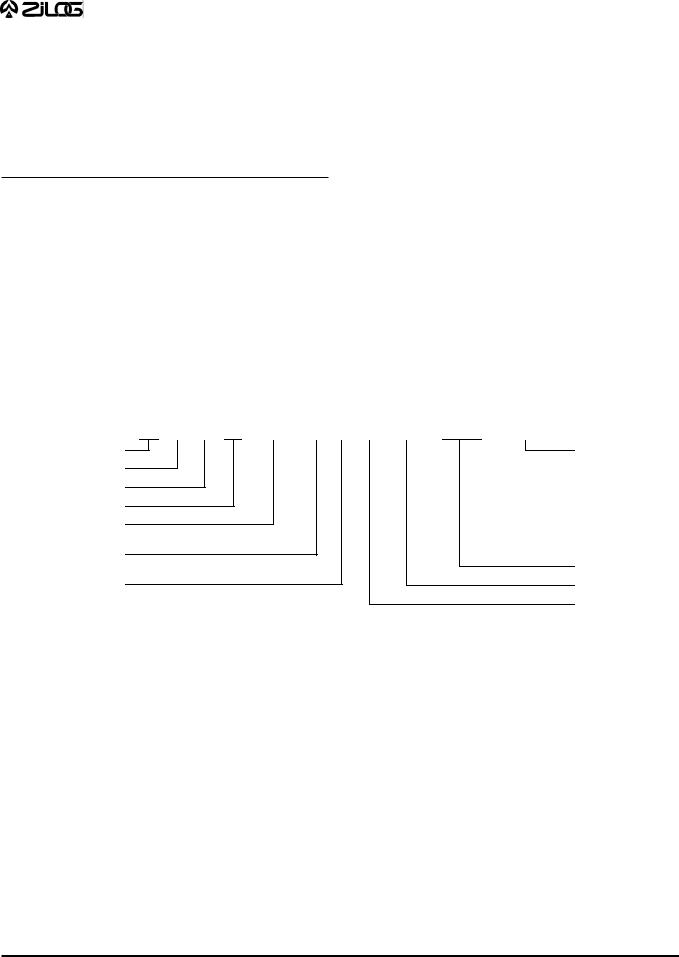
P R E L I M I N A R Y |
Z89323/373/393 |
16-BIT DIGITAL SIGNAL PROCESSORS |
REGISTERS (Continued)
The Status Register
The status register can always be read in its entirety. S15S10 are set/reset by hardware and can only be read by software. S9-S0 control hardware looping and can be written by software (Table 8).
Table 8. RPL Description
S2 |
S1 |
S0 |
Loop Size |
|
|
|
|
0 |
0 |
0 |
256 |
0 |
0 |
1 |
2 |
0 |
1 |
0 |
4 |
0 |
1 |
1 |
8 |
|
|
|
|
1 |
0 |
0 |
1 6 |
1 |
0 |
1 |
3 2 |
1 |
1 |
0 |
6 4 |
1 |
1 |
1 |
128 |
|
|
|
|
S15-S12 are set/reset by the ALU after an operation. S11S10 are set/reset by the user inputs. S6-S0 are control bits described in Table 5. S7 enables interrupts. If S8 is set, the hardware clamps at maximum positive or negative values instead of overflowing. If S9 is set and a multiple/shift option is used, then the shifter shifts the result three bits right. This feature allows the data to be scaled and prevents overflows.
PC is the Program Counter. When this register is assigned as a destination register, one NOP machine cycle is added automatically to adjust the pipeline timing.
Negative
Overflow
Zero
Carry
User Input 0-1
(Read Only)
MPY output arithmetically shifted right by three bits
Overflow protection
N |
|
OV |
|
Z |
C |
|
UI1 |
UI0 |
SH3 |
|
OP |
|
IE |
UO1 UO0 |
|
|
|
|
RPL |
|
|
||||||||
S15 |
|
S14 |
|
S13 |
S12 |
|
S11 |
S10 |
|
S9 |
|
S8 |
|
S7 |
|
S6 |
S5 |
S4 |
S3 |
|
S2 |
S1 |
S0 |
||||||
|
|
|
|
|
|
|
|
|
|
|
|
|
|
|
|
|
|
|
|
|
|
|
|
|
|
|
|
|
|
|
|
|
|
|
|
|
|
|
|
|
|
|
|
|
|
|
|
|
|
|
|
|
|
|
|
|
|
|
|
Ram |
Loop |
Pointer |
Size |
0 0 0 |
256 |
0 0 1 |
2 |
0 1 0 |
4 |
0 1 1 |
8 |
1 0 0 |
16 |
1 0 1 |
32 |
1 1 0 |
64 |
1 1 1 |
128 |
"Short Form Direct" bits
User Output 0-1*
Global Interrupt Enable
* The output value is the opposite of the status register content.
Figure 7. Status Register
14 |
DS95DSP0101 Q4/95 |

P R E L I M I N A R Y |
Z89323/373/393 |
16-BIT DIGITAL SIGNAL PROCESSORS |
EXT Register Assignments
The EXT registers support is extended in the Z893X3 family: In addition to up to seven external registers, there are 28 internal registers on the EXT bus. There are 16 different pages of EXT registers. The same EXT7 register exist in all the pages and control of the bank switching is done via EXT7 register.
Banks 0 to 5 support different combinations of external registers and internal data registers. The user should use the bank that has the internal data registers and the number of external registers to support his application and to use this bank as a working bank to minimize the number of bank switching. Bank 5 has all the A/D registers. Banks 13 to 15 are control registers bank. These control registers are usually used only in the initialization routines.
Table 6. EXT Register Assignments Banks 0–4
EXT\Bank |
0 |
1 |
2 |
3 |
4 |
|
|
|
|
|
|
EXT0 |
Ext0-user |
Ext0-user |
Ext0-user |
Ext0-user |
Ext0-user |
EXT1 |
Ext1-user |
Ext1-user |
Ext1-user |
Ext1-user |
Ext1-user |
EXT2 |
Ext2-user |
Ext2-user |
Ext2-user |
Ext2-user |
Ext2-user |
EXT3 |
SPI data |
Ext3-user |
Ext3-user |
SPI data |
Ext3-user |
|
|
|
|
|
|
EXT4 |
Port0 |
Port0 |
Ext4-user |
Ext4-user |
Ext4-user |
EXT5 |
Port1/Port2 |
Port1/Port2 |
Port3 |
Ext5-user |
Ext5-user |
EXT6 |
A/D_ch0 |
A/D_ch1 |
A/D_ch2 |
A/D_ch3 |
Ext6-user |
EXT7 |
Bank/Int_status |
Bank/Int_status |
Bank/Int_status |
Bank/Int_status |
Bank/Int_status |
|
|
|
|
|
|
Table 7. EXT Register Assignments Banks 6–15
EXT\Bank |
5 |
6-12 |
13 |
|
14 |
|
15 |
|
|
|
|
|
|
|
|
||
EXT0 |
A/D_ch1 |
|
A/D control |
Timer2 load |
P0 |
control |
||
EXT1 |
A/D_ch2 |
|
Timer0 control |
Timer1 control |
P1 |
control |
||
EXT2 |
A/D_ch3 |
|
Timer0 load |
Timer1 load |
P2 |
control |
||
EXT3 |
SPI data |
|
Timer0 |
|
Timer1 |
|
Wait State |
|
EXT4 |
Port0 |
|
Timer0 |
pr. load |
Timer1 |
pr. load |
SPI control |
|
EXT5 |
Port1/Port2 |
|
Timer0 |
prescaler |
Timer1 |
prescaler |
PLL control |
|
EXT6 |
A/D_ch0 |
A/D_ch0 |
A/D_ch0 |
A/D_ch0 |
Int. Allocation |
|||
EXT7 |
Bank/Int_status |
Bank/Int_status |
Bank/Int_status |
Bank/Int_status |
Bank/Int_status |
|||
|
|
|
|
|
|
|
|
|
DS95DSP0101 Q4/95 |
15 |
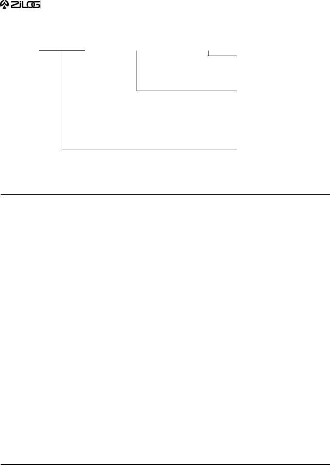
P R E L I M I N A R Y |
Z89323/373/393 |
16-BIT DIGITAL SIGNAL PROCESSORS |
EXT Register Assignments (Continued)
Ext 7 Reg
D15 |
D14 |
D13 |
D12 |
|
D11 |
D10 |
D9 |
D8 |
D7 |
D6 |
D5 |
D4 |
|
D3 |
D2 |
D1 |
D0 |
||
|
|
|
|
|
|
|
|
|
|
|
|
|
|
|
|
|
|
|
|
|
|
|
|
|
|
|
|
|
|
|
|
|
|
|
|
|
|
|
|
Bank Select
0000 : Bank0
0001 : Bank1
:
:
1111 : Bank15
Interrupt Status Bits
Bit 4 = A/D Finish Interrupt
Bit 5 = SPI Interrupt
Bit 6 = Timer0 Interrupt
Bit 7 = Timer1 Interrupt
Bit 8 = Timer2 Interrupt
Bit 9 = INT0 (H/W) Interrupt
Bit 10 = INT1 (H/W) Interrupt
Bit 11 = INT2 (H/W) Interrupt
Reserved
Figure 8. EXT7 Register Bit Assignment
Interrupt Status Bits
When read, these bits provide interrupt information to identify the source for INT2, or when the DSP works in Pending Interrupt mode, to warn the DSP of pending interrupts. These bits also clear the interrupt status bits. Writing 1 will clear these bits.
Wait-State Register
The Wait-State Control Register enables insertion of Wait States when the DSP needs to access slow, inexpensive peripherals. This software-controlled register enables insertion of one Wait State when accessing EXT bus. (One Wait State gives 100 nsec access time instead of 50 nsec
access time with a 20 MHz oscillator.) When more than one Wait State is needed, an input pin (WAIT) coupled with external logic can support more than one Wait State. The Wait-State Control Register enables mapping specific EXT register (from EXT0 to EXT6) and specific operation (read or write) to include insertion of one Wait State. EXT7 is always internal register, therefore no Wait State is needed for EXT7.
Note:
When the programmer switches banks it is important to change the Wait State mapping of the EXT registers to match the desired Wait State mapping of the new bank.
16 |
DS95DSP0101 Q4/95 |

|
|
|
|
|
|
|
|
|
|
|
|
|
|
|
P R E L I M I N A R Y |
|
|
|
|
Z89323/373/393 |
||||||||||||
|
|
|
|
|
|
|
|
|
|
|
|
|
|
|
|
|
|
16-BIT DIGITAL SIGNAL PROCESSORS |
||||||||||||||
|
Bank15/EXT3 Reg |
|
|
|
|
|
|
|
|
|
|
|
|
|
|
|
|
|
|
|
|
|
|
|
|
|
|
|||||
|
D15 |
D14 |
|
|
D13 |
D12 |
|
D11 |
D10 |
D9 |
D8 |
|
D7 |
D6 |
|
D5 |
D4 |
|
D3 |
D2 |
D1 |
D0 |
|
|
|
|||||||
|
|
|
|
|
|
|
|
|
|
|
|
|
|
|
|
|
|
|
|
|
|
|
|
|
|
|
|
|
|
Bits 1 - 0 = Wait-State EXT0 |
||
|
|
|
|
|
|
|
|
|
|
|
|
|
|
|
|
|
|
|
|
|
|
|
|
|
|
|
|
|
|
|||
|
|
|
|
|
|
|
|
|
|
|
|
|
|
|
|
|
|
|
|
|
|
|
|
|
|
|
|
|
|
|||
|
|
|
|
|
|
|
|
|
|
|
|
|
|
|
|
|
|
|
|
|
|
|
|
|
|
|
|
|
|
|||
|
|
|
|
|
|
|
|
|
|
|
|
|
|
|
|
|
|
|
|
|
|
|
|
|
|
|
|
|
|
Bits 3 - 2 = Wait-State |
EXT1 |
|
|
|
|
|
|
|
|
|
|
|
|
|
|
|
|
|
|
|
|
|
|
|
|
|
|
|
|
|
|
|
|||
|
|
|
|
|
|
|
|
|
|
|
|
|
|
|
|
|
|
|
|
|
|
|
|
|
|
|
|
|
|
Bits 5 - 4 = Wait-State |
EXT2 |
|
|
|
|
|
|
|
|
|
|
|
|
|
|
|
|
|
|
|
|
|
|
|
|
|
|
|
|
|
|
|
|||
|
|
|
|
|
|
|
|
|
|
|
|
|
|
|
|
|
|
|
|
|
|
|
|
|
|
|
|
|
|
Bits 7 - 6 = Wait-State |
EXT3 |
|
|
|
|
|
|
|
|
|
|
|
|
|
|
|
|
|
|
|
|
|
|
|
|
|
|
|
|
|
|
|
|||
|
|
|
|
|
|
|
|
|
|
|
|
|
|
|
|
|
|
|
|
|
|
|
|
|
|
|
|
|
|
Bits 9 - 8 = Wait-State |
EXT4 |
|
|
|
|
|
|
|
|
|
|
|
|
|
|
|
|
|
|
|
|
|
|
|
|
|
|
|
|
|
|
|
|||
|
|
|
|
|
|
|
|
|
|
|
|
|
|
|
|
|
|
|
|
|
|
|
|
|
|
|
|
|
|
Bits 11 -10 = Wait-State |
EXT5 |
|
|
|
|
|
|
|
|
|
|
|
|
|
|
|
|
|
|
|
|
|
|
|
|
|
|
|
|
|
|
|
|||
|
|
|
|
|
|
|
|
|
|
|
|
|
|
|
|
|
|
|
|
|
|
|
|
|
|
|
|
|
|
Bits 13 -12 = Wait-State |
EXT6 |
|
|
|
|
|
|
|
|
|
|
|
|
|
|
|
|
|
|
|
|
|
|
|
|
|
|
|
|
|
|
|
|||
|
|
|
|
|
|
|
|
|
|
|
|
|
|
|
|
|
|
|
|
|
|
|
|
|
|
|
|
|
|
Bit14 = Reserved |
|
|
|
|
|
|
|
|
|
|
|
|
|
|
|
|
|
|
|
|
|
|
|
|
|
|
|
|
|
|
|
|
|
|
|
|
|
|
|
|
|
|
|
|
|
|
|
|
|
|
|
|
|
|
|
|
|
|
|
|
|
|
|
|
|
Bit 15 = Test Mode |
|
|
0 Normal Operation (default)
1 Test Mode: Bits 6-5 of the
Status Register drives,
P23 and P22, respectively
(VO0 and VO1).
Figure 8a. Bank 15/EXT3 Register
DS95DSP0101 Q4/95 |
17 |

P R E L I M I N A R Y |
Z89323/373/393 |
16-BIT DIGITAL SIGNAL PROCESSORS |
FUNCTIONAL DESCRIPTION
Analog to Digital Converter (ADC)
The ADC is an 8-bit half flash converter that uses two reference resistor ladders for its upper 4 bits (Most Significant Bits) and lower 4 bits (Least Significant Bits) conversion. Two reference voltage pins, VA (High) and VA (Low), are provided for external reference voltage supplies. During the sampling period from one of the four channel inputs, the converter is also being auto-zeroed before starting the conversion. The conversion time is dependent on the external clock frequency and the selection of the prescaler value for the internal ADC clock source. The minimum conversion time is 2.0 μs. (See Figure 9, ADC Architecture.)
The ADC control register is Bank 13/Ext 0. A conversion can be initiated in one of four ways: by writing to the A/D control register, INT1 input pin, Timer 2 or Timer 0 equal 0. These four are programmable selectable. There are four modes of operation that can be selected: one channel converted four times with the results written to each Result register, one channel continuously converted and one Result channel updated for each conversion, four channels converted once each and the four results written to the Result registers, and four channels repeatedly converted and the Result registers kept updated. The channel to be converted is programmable and if one of the four-channel modes is selected then the programmed channel will be the first channel converted and the other three will be in sequence following with wraparound from Channel 3 to Channel 0.
The start commands are implemented in such a way as to begin a conversion at any time, if a conversion is in progress and a new start command is received, then the conversion in progress will be aborted and a new conversion will be initiated. This allows the programmed values to be changed without affecting a conversion-in-progress. The new values will take effect only after a new start command is received.
The clock prescaler can be programmed to derive a minimum 2 μs conversion time for clock inputs from 4 MHz to 20 MHz. For example, with a 20 MHz crystal clock the prescaler should be programmed for divide by 40, which then gives a 2 μs conversion rate.
The ADC can generate an Interrupt after either the first or fourth conversion is complete depending on the programmable selection.
The ADC can be disabled (for low power) or enabled by a Control Register bit.
Though the ADC will function for a smaller input voltage and voltage reference, the noise and offsets remain constant during the specified electrical range. The errors of the converter will increase and the conversion time may also take slightly longer due to smaller input signals.
18 |
DS95DSP0101 Q4/95 |

P R E L I M I N A R Y |
Z89323/373/393 |
|||||||
16-BIT DIGITAL SIGNAL PROCESSORS |
||||||||
INT0 Timer |
|
|||||||
|
|
|
|
|
|
|
|
|
|
|
Start |
|
|
|
|
Converter |
|
|
|
|
|
A/D |
|
|
|
|
Controller |
|
|
|
A/D |
Register |
|
|
|
Prescaler |
|
|
Integrated |
|
|
|
|
Logic |
|
|
|
|
|
VREF |
|
4x8 |
Internal |
|
|
|
Bus |
|
|
|
|
Result |
|
|
|
|
|
|
|
|
|
Register |
|
4-Channel |
Sample |
Flash |
|
|
Multiplexer |
A/D |
|
|
|
|
and |
Converter |
|
|
|
Hold |
|
|
|
AGND |
Dual |
A/D |
|
|
Channel |
|
Scan |
Register |
|
|
|
|
Channel Select |
|
Figure 9. ADC Architecture
DS95DSP0101 Q4/95 |
19 |
 Loading...